CMOS Detectors Ingeniously Simple!
|
|
|
- Doreen Farmer
- 6 years ago
- Views:
Transcription


1 CMOS Detectors Ingeniously Simple! A.Schöning University Heidelberg B-Workshop Neckarzimmern

2 Detector System on Chip? 2
3 ATLAS Pixel Module 3

4 ATLAS Pixel Module MCC sensor FE-Chip FE-Chip 4

5 ATLAS Insertable B-Layer 5


6 ATLAS Pixel Module FE chip ~250 µm ~ e 6
7 Silicon Hybrid Detectors Features high signal and high noise complex compound bump bonding wire wrapping custom-made sensor lots of material (radiation lengths!) MCC sensor FE-Chip FE-Chip expensive (e.g. ATLAS II pixel HW: 16 mill.chf for ~5m2) scalability problem (e.g. Future experiments at FCC) miniaturization problem >108/m2 bump bonds? quality assurance problem 7
 CMOS (intelligence)")
8 Silicon Detector cables sensor (silicon) CMOS (intelligence) (cooling) 8
9 Silicon Detector CMOS chip no composite no interconnects simplified design (ASIC design) profits from miniaturisation System on a chip 9
10 CMOS Features minimum pixel size feature size 5µm possible!!! low power (CMOS) low noise compared to hybrids compact VLSI design standard process cheap 10

11 Dopings n-type p-type electrons are majority charge carriers holes are majority charge carriers 11

 p-channel MOSFET (PMOS)")

12 What is CMOS? Complementary Metal Oxide Semiconductors n-channel MOSFET (NMOS) p-channel MOSFET (PMOS) MOSFET= metal oxide semiconductor field effect transistor Metal-Isolator-Semiconductor (MISFIT)- structure 12

 MOSFET=metal oxide semiconductor")
13 What is CMOS? Complementary Metal Oxide Semiconductors n-channel MOSFET (NMOS) p-channel MOSFET (PMOS) MOSFET=metal oxide semiconductor field effect transistor n-channel (NMOS) 13


14 Advantages of CMOS fast switching characteristics used for CPUs no ohmic resistors needed low power easy to implement capacitors PMOS NMOS CMOS Inverter 14
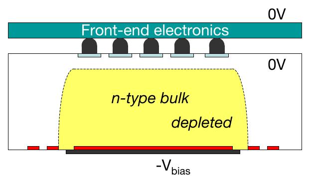
15 Monolithic Active Pixel Sensors (MAPS) How to design a CMOS particle detector? particle monolithic = single process problem: low resistivity fast recombination small charge collection 15
16 The MAPS Principle D.Husson, NIMA 461 (2001) MIMOSA = Minimum Ionizing MOS Active pixel sensor ~15 μm 80 e- per μm p- space charge diffusion random walk recombination! time scale: τ ~ 100 ns p++ voltage ~3V 16
17 MIMOSA Schema pixel outside pixel Idea dates back to the 1980ies SSC reset source follower sensor readout control Sh. Parker, NIMA 275 (1989) 494 Challenge: separation of analog and control signals e.g. readout control should not affect signal Berst et al. (1999) 17
 on sensor!")
18 MIMOSA Pixel Layout 1-diode pixel 4-diode pixel transistors (intelligence) on sensor! 18
19 Rolling Shutter MAPS Readout Turchetta et al. NIMA 458 (2000) 677 analogue output discriminator 64 x 64 array 20 x 20 μm2 19

20 MIMOSA: Energy Distribution Berst et al., LEPSI x 3 pixel á 20 x 20 μm2 20
21 The charge collection efficiency D. Husson, NIMA 461 (2001) 511 Simulation 0.6 μm process ENC = ~ 20e- charge is spread over many pixels! ENC = equivalent noise charge 21
22 MAPS Charge Collection Time Berst et al. (2001) 5 µm 20 µm 22
23 Noise in CMOS Sensors usually dominant source is the so called Reset or Capacitive Noise: kt V RMS = C Q = C V RMS n RMS = ktc e typical signal over noise: S/N=20-50 Other sources: thermal noise S ν (w) = 4kTR shot noise flickering noise (1/f) 23

 new ALICE vertex detector (~ 10 m2)")

24 MAPS Applications MIMOSA originally proposed for ILD vertex detector used in DESY Aconite telescope (EUDET) STAR vertex detector (350 mill. pixel) new ALICE vertex detector (~ 10 m2) applications where time resolution is not an serious issue STAR 0.16 m2 MAPS BILDER Aconite (DESY) ALICE 7 layers of MAPS 24
 876 Floating structure")

25 High Voltage MAPS Ivan Perić, NIMA 582 (2007) 876 Floating structure MOSFETS in well 100% fill factor high depletion at 50 V Low Voltage HV 25

26 HV-MAPS Pixel Design ~ µm Fast circuit and thin sensor! DAC = digital to analog converter adjustment of threshold 26
 limited hit resolution regime multiple scattering regime multiple scattering")
27 HV-MAPS and Multiple Scattering HV-MAPS: allow for small pixel sizes can measure very low momentum tracks (thin sensor) limited hit resolution regime multiple scattering regime multiple scattering regime 27

28 Mu3e Experiment Search for µ+ e+ e+ e- (signal) Background: µ+ e+ v v p(e+) < 53 MeV µ+ ~ 1 muon decay / ns Fast and very thin detector required MuPix sensor 28

29 Mupix Chip 29
30 Mupix Chip Mupix7 prototype: ~ 3 x 3 mm2 ~1200 pixels pixel size ~ 80 x 100 µm2 Mupix7 features: Tune DACS for every pixel double stage amplifier (every pixel) zero suppression timestamp generation up to ~100 MHz 10 ns 1.2 GHz PLL integrated 1.2 (2.4) Gbit/s link about 40 pads needed (wire bond) System on Chip! 30


31 Mupix Readout Design Mupix7 prototype: ~ 3 x 3 mm2 ~1200 pixels pixel size ~ 80 x 100 µm2 Readout periphery 46 µm Comparator 7µm DAC and SRAM Coupling capacitor Address ROM TS DRAM CMOS digital part 31
32 MuPix Time Resolution DESY Testbeam with 5 GeV electrons includes time resolution of setup and sampling fastest monolithic pixel sensor! 32
33 MuPix Time Resolution signal height PSI Testbeam with 500 MeV protons timewalk correction possible 33

34 MuPix Pixel Efficiency Efficiency > 99.5% 34
35 MuPix Requirements 35


36 MuPix Tracker Construction Ultra-thin detector mock-up: sandwich of 25 µm Kapton 50/100 µm glass (instead of Si) 50 mu silicon wafer Sandwich X/X0 ~ 0.1% per layer 36
37 Summary CMOS detectors = System on Chip provides very thin sensors and small pixels used and/or considered for many upgrade projects HV-CMOS (HV-MAPS) solves timing and rate issues clearly the way to go in future! 37
 costs ~130 MCHF 14 tracking layers (10 strip + 4 pixel)")

38 Outlook HV-MAPS for LHC or FCC experiments? ATLAS II tracker (ITK) costs ~130 MCHF 14 tracking layers (10 strip + 4 pixel) X/X0 ~ 1-2% per layer ATLAS stereo strip module HV-MAPS Pixel only tracker? only 6-9 pixel layers required % per radiation length reduced material costs reduced assembly costs 3D tracking performance 38
39 BACKUP 39
40 Pulse Shape Measurement with ToT ToT= time over threshold 40
41 Noise Measurement with Threshold Scan 41

42 Silicon on Insulator (SOI) Concept CMOS buried oxide layer (insulator) depletion zone depletion ~50 um signal ~ 3000e noise ~ 30e higher radiation tolerance with n-well and p-well T.Hemperek et al. (Bonn) 42
43 Austria Microsystems (AMS) High-Voltage CMOS technology H18 process 0.18 um available since March V, 5V, 20V and 50V devices on a single chip without any process modifications 43
44 Mu3e Baseline Design Long cylinder! not to scale ~180 cm ~15 cm B = 1 Tesla 44
The High-Voltage Monolithic Active Pixel Sensor for the Mu3e Experiment
 The High-Voltage Monolithic Active Pixel Sensor for the Mu3e Experiment Shruti Shrestha On Behalf of the Mu3e Collaboration International Conference on Technology and Instrumentation in Particle Physics
Track Triggers for ATLAS
 Track Triggers for ATLAS André Schöning University Heidelberg 10. Terascale Detector Workshop DESY 10.-13. April 2017 from https://www.enterprisedb.com/blog/3-ways-reduce-it-complexitydigital-transformation
Strip Detectors. Principal: Silicon strip detector. Ingrid--MariaGregor,SemiconductorsasParticleDetectors. metallization (Al) p +--strips
 p +--strips") Strip Detectors First detector devices using the lithographic capabilities of microelectronics First Silicon detectors -- > strip detectors Can be found in all high energy physics experiments of the last
Strip Detectors First detector devices using the lithographic capabilities of microelectronics First Silicon detectors -- > strip detectors Can be found in all high energy physics experiments of the last
A new strips tracker for the upgraded ATLAS ITk detector
 A new strips tracker for the upgraded ATLAS ITk detector, on behalf of the ATLAS Collaboration : 11th International Conference on Position Sensitive Detectors 3-7 The Open University, Milton Keynes, UK.
ITk silicon strips detector test beam at DESY
 ITk silicon strips detector test beam at DESY Lucrezia Stella Bruni Nikhef Nikhef ATLAS outing 29/05/2015 L. S. Bruni - Nikhef 1 / 11 Qualification task I Participation at the ITk silicon strip test beams
Muon detection in security applications and monolithic active pixel sensors
 Muon detection in security applications and monolithic active pixel sensors Tracking in particle physics Gaseous detectors Silicon strips Silicon pixels Monolithic active pixel sensors Cosmic Muon tomography
Lecture 2. Part 2 (Semiconductor detectors =sensors + electronics) Segmented detectors with pn-junction. Strip/pixel detectors
 Segmented detectors with pn-junction. Strip/pixel detectors") Lecture 2 Part 1 (Electronics) Signal formation Readout electronics Noise Part 2 (Semiconductor detectors =sensors + electronics) Segmented detectors with pn-junction Strip/pixel detectors Drift detectors
Lecture 2 Part 1 (Electronics) Signal formation Readout electronics Noise Part 2 (Semiconductor detectors =sensors + electronics) Segmented detectors with pn-junction Strip/pixel detectors Drift detectors
MAPS-based ECAL Option for ILC
 MAPS-based ECAL Option for ILC, Spain Konstantin Stefanov On behalf of J. Crooks, P. Dauncey, A.-M. Magnan, Y. Mikami, R. Turchetta, M. Tyndel, G. Villani, N. Watson, J. Wilson v Introduction v ECAL with
High Luminosity ATLAS vs. CMOS Sensors
 High Luminosity ATLAS vs. CMOS Sensors Where we currently are and where we d like to be Jens Dopke, STFC RAL 1 Disclaimer I usually do talks on things where I generated all the imagery myself (ATLAS Pixels/IBL)
Towards a 10 μs, thin high resolution pixelated CMOS sensor system for future vertex detectors
 Towards a 10 μs, thin high resolution pixelated CMOS sensor system for future vertex detectors Rita De Masi IPHC-Strasbourg On behalf of the IPHC-IRFU collaboration Physics motivations. Principle of operation
Meeting with STM HV-CMOS
 Meeting with STM HV-CMOS!! Giovanni Darbo INFN- Genova o Credits: Most of the material in these slides come from presenta
Semiconductor Detector Systems
 Semiconductor Detector Systems Helmuth Spieler Physics Division, Lawrence Berkeley National Laboratory OXFORD UNIVERSITY PRESS ix CONTENTS 1 Detector systems overview 1 1.1 Sensor 2 1.2 Preamplifier 3
HV-MAPS. Dirk Wiedner Physikalisches Institut der Universität Heidelberg on behalf of the Mu3e silicon detector collaboration
 HV-MAPS Dirk Wiedner Physikalisches Institut der Universität Heidelberg on behalf of the Mu3e silicon detector collaboration 1 From Tracking to Pixel Sensors 2 Decay point o Primary vertex: o Tracks of
Pixel sensors with different pitch layouts for ATLAS Phase-II upgrade
 Pixel sensors with different pitch layouts for ATLAS Phase-II upgrade Different pitch layouts are considered for the pixel detector being designed for the ATLAS upgraded tracking system which will be operating
Radiation-hard active CMOS pixel sensors for HL- LHC detector upgrades
 Journal of Instrumentation OPEN ACCESS Radiation-hard active CMOS pixel sensors for HL- LHC detector upgrades To cite this article: Malte Backhaus Recent citations - Module and electronics developments
New fabrication and packaging technologies for CMOS pixel sensors: closing gap between hybrid and monolithic
 New fabrication and packaging technologies for CMOS pixel sensors: closing gap between hybrid and monolithic Outline Short history of MAPS development at IPHC Results from TowerJazz CIS test sensor Ultra-thin
A monolithic pixel sensor with fine space-time resolution based on silicon-on-insulator technology for the ILC vertex detector
 A monolithic pixel sensor with fine space-time resolution based on silicon-on-insulator technology for the ILC vertex detector, Miho Yamada, Toru Tsuboyama, Yasuo Arai, Ikuo Kurachi High Energy Accelerator
Monolithic Pixel Sensors in SOI technology R&D activities at LBNL
 Monolithic Pixel Sensors in SOI technology R&D activities at LBNL Lawrence Berkeley National Laboratory M. Battaglia, L. Glesener (UC Berkeley & LBNL), D. Bisello, P. Giubilato (LBNL & INFN Padova), P.
SOFIST ver.2 for the ILC vertex detector
 SOFIST ver.2 for the ILC vertex detector Proposal of SOI sensor for ILC: SOFIST SOI sensor for Fine measurement of Space and Time Miho Yamada (KEK) IHEP Mini Workshop at IHEP Beijing 2016/07/15 SOFIST ver.2
Chapter 4 Vertex. Qun Ouyang. Nov.10 th, 2017Beijing. CEPC detector CDR mini-review
 Chapter 4 Vertex Qun Ouyang Nov.10 th, 2017Beijing Nov.10 h, 2017 CEPC detector CDR mini-review CEPC detector CDR mini-review Contents: 4 Vertex Detector 4.1 Performance Requirements and Detector Challenges
UFSD: Ultra-Fast Silicon Detector
 UFSD: Ultra-Fast Silicon Detector Basic goals of UFSD (aka Low-Gain Avalanche Diode) A parameterization of time resolution State of the art How to do better Overview of the sensor design Example of application
Development of CMOS pixel sensors for tracking and vertexing in high energy physics experiments
 PICSEL group Development of CMOS pixel sensors for tracking and vertexing in high energy physics experiments Serhiy Senyukov (IPHC-CNRS Strasbourg) on behalf of the PICSEL group 7th October 2013 IPRD13,
Development of Pixel Detectors for the Inner Tracker Upgrade of the ATLAS Experiment
 Development of Pixel Detectors for the Inner Tracker Upgrade of the ATLAS Experiment Natascha Savić L. Bergbreiter, J. Breuer, A. Macchiolo, R. Nisius, S. Terzo IMPRS, Munich # 29.5.215 Franz Dinkelacker
arxiv: v1 [physics.ins-det] 26 Nov 2015
![arxiv: v1 [physics.ins-det] 26 Nov 2015](/thumbs/91/104762493.jpg "arxiv: v1 [physics.ins-det] 26 Nov 2015") arxiv:1511.08368v1 [physics.ins-det] 26 Nov 2015 European Organization for Nuclear Research (CERN), Switzerland and Utrecht University, Netherlands E-mail: monika.kofarago@cern.ch The upgrade of the Inner
arxiv:1511.08368v1 [physics.ins-det] 26 Nov 2015 European Organization for Nuclear Research (CERN), Switzerland and Utrecht University, Netherlands E-mail: monika.kofarago@cern.ch The upgrade of the Inner
Status of ATLAS & CMS Experiments
 Status of ATLAS & CMS Experiments Atlas S.C. Magnet system Large Air-Core Toroids for µ Tracking 2Tesla Solenoid for inner Tracking (7*2.5m) ECAL & HCAL outside Solenoid Solenoid integrated in ECAL Barrel
ATLAS strip detector upgrade for the HL-LHC
 ATL-INDET-PROC-2015-010 26 August 2015, On behalf of the ATLAS collaboration Santa Cruz Institute for Particle Physics, University of California, Santa Cruz E-mail: zhijun.liang@cern.ch Beginning in 2024,
Radiation Tolerance of HV-CMOS Sensors
 Radiation Tolerance of HV-CMOS Sensors Ivan Perić, Ann-Kathrin Perrevoort, Heiko Augustin, Niklaus Berger, Dirk Wiedner, Michael Deveaux, Alexander Dierlamm, Franz Wagner, Frederic Bompard, Patrick Breugnon,
Towards Monolithic Pixel Detectors for ATLAS HL-LHC Upgrades
 Towards Monolithic Pixel Detectors for ATLAS HL-LHC Upgrades Hans Krüger Bonn University FEE 2016 Meeting, Krakow Outline Comparison of Pixel Detector Technologies for HL-LHC upgrades (ATLAS) Design Challenges
A Prototype Amplifier-Discriminator Chip for the GLAST Silicon-Strip Tracker
 A Prototype Amplifier-Discriminator Chip for the GLAST Silicon-Strip Tracker Robert P. Johnson Pavel Poplevin Hartmut Sadrozinski Ned Spencer Santa Cruz Institute for Particle Physics The GLAST Project
 http://clicdp.cern.ch Hybrid Pixel Detectors with Active-Edge Sensors for the CLIC Vertex Detector Simon Spannagel on behalf of the CLICdp Collaboration Experimental Conditions at CLIC CLIC beam structure
Pixel hybrid photon detectors
 Pixel hybrid photon detectors for the LHCb-RICH system Ken Wyllie On behalf of the LHCb-RICH group CERN, Geneva, Switzerland 1 Outline of the talk Introduction The LHCb detector The RICH 2 counter Overall
Pixel characterization for the ITS/MFT upgrade. Audrey Francisco
 Pixel characterization for the ITS/MFT upgrade Audrey Francisco QGP France, Etretat, 14/10/2015 Outline 1 The MFT upgrade 2 Pixel sensor Technology choice Full scale prototypes 3 Characterization campaign
CMOS pixel sensors developments in Strasbourg
 SuperB XVII Workshop + Kick Off Meeting La Biodola, May 2011 CMOS pixel sensors developments in Strasbourg Outline sensor performances assessment state of the art: MIMOSA-26 and its applications Strasbourg
arxiv: v2 [physics.ins-det] 15 Nov 2017
![arxiv: v2 [physics.ins-det] 15 Nov 2017](/thumbs/78/78227975.jpg "arxiv: v2 [physics.ins-det] 15 Nov 2017") Development of depleted monolithic pixel sensors in 150 nm CMOS technology for the ATLAS Inner Tracker upgrade arxiv:1711.01233v2 [physics.ins-det] 15 Nov 2017 P. Rymaszewski a, M. Barbero b, S. Bhat b,
Development of depleted monolithic pixel sensors in 150 nm CMOS technology for the ATLAS Inner Tracker upgrade arxiv:1711.01233v2 [physics.ins-det] 15 Nov 2017 P. Rymaszewski a, M. Barbero b, S. Bhat b,
Mu3e. Dirk Wiedner, Heidelberg On Behalf of the Mu3e Collaboration. Dirk Wiedner, on behalf of the Mu3e collaboration
 Mu3e Dirk Wiedner, Heidelberg On Behalf of the Mu3e Collaboration 1 The Mu3e Signal μ + e + e - e + rare in νsm o Branching ratio
Thin Silicon R&D for LC applications
 Thin Silicon R&D for LC applications D. Bortoletto Purdue University Status report Hybrid Pixel Detectors for LC Next Linear Collider:Physic requirements Vertexing 10 µ mgev σ r φ,z(ip ) 5µ m 3 / 2 p sin
X-ray Detectors: What are the Needs?
 X-ray Detectors: What are the Needs? Sol M. Gruner Physics Dept. & Cornell High Energy Synchrotron Source (CHESS) Ithaca, NY 14853 smg26@cornell.edu 1 simplified view of the Evolution of Imaging Synchrotron
Towards a 10μs, thin high resolution pixelated CMOS sensor for future vertex detectors
 Towards a 10μs, thin high resolution pixelated CMOS sensor for future vertex detectors Yorgos Voutsinas IPHC Strasbourg on behalf of IPHC IRFU collaboration CMOS sensors principles Physics motivations
Layout and prototyping of the new ATLAS Inner Tracker for the High Luminosity LHC
 Layout and prototyping of the new ATLAS Inner Tracker for the High Luminosity LHC Ankush Mitra, University of Warwick, UK on behalf of the ATLAS ITk Collaboration PSD11 : The 11th International Conference
The Belle II Vertex Pixel Detector
 The Belle II Vertex Pixel Detector IMPRS Young Scientist Workshop July 16-19, 2014 Ringberg Castle Kreuth, Germany Felix Mueller 1 fmu@mpp.mpg.de Outline SuperKEKB and Belle II Vertex Detector (VXD) Pixel
A High Granularity Timing Detector for the Phase II Upgrade of the ATLAS experiment
 3 rd Workshop on LHCbUpgrade II LAPP, 22 23 March 2017 A High Granularity Timing Detector for the Phase II Upgrade of the ATLAS experiment Evangelos Leonidas Gkougkousis On behalf of the ATLAS HGTD community
A High-Granularity Timing Detector for the Phase-II upgrade of the ATLAS Detector system
 A High-Granularity Timing Detector for the Phase-II upgrade of the ATLAS Detector system C.Agapopoulou on behalf of the ATLAS Lar -HGTD group 2017 IEEE Nuclear Science Symposium and Medical Imaging Conference
UFSD: Ultra-Fast Silicon Detector
 UFSD: Ultra-Fast Silicon Detector Basic goals of UFSD A parameterization of time resolution State of the art How to do better Overview of the sensor design First Results Nicolo Cartiglia with M. Baselga,
3D activities and plans in Italian HEP labs Valerio Re INFN Pavia and University of Bergamo
 3D activities and plans in Italian HEP labs Valerio Re INFN Pavia and University of Bergamo 1 Vertical integration technologies in Italian R&D programs In Italy, so far interest for 3D vertical integration
Silicon Detectors in High Energy Physics
 Thomas Bergauer (HEPHY Vienna) IPM Teheran 22 May 2011 Sunday: Schedule Semiconductor Basics (45 ) Silicon Detectors in Detector concepts: Pixels and Strips (45 ) Coffee Break Strip Detector Performance
A High-Granularity Timing Detector for the Phase-II upgrade of the ATLAS Calorimeter system Detector concept description and first beam test results
 A High-Granularity Timing Detector for the Phase-II upgrade of the ATLAS Calorimeter system Detector concept description and first beam test results 03/10/2017 ATL-LARG-SLIDE-2017-858 Didier Lacour On
CMS Tracker Upgrades. R&D Plans, Present Status and Perspectives. Benedikt Vormwald Hamburg University on behalf of the CMS collaboration
 R&D Plans, Present Status and Perspectives Benedikt Vormwald Hamburg University on behalf of the CMS collaboration EPS-HEP 2015 Vienna, 22.-29.07.2015 CMS Tracker Upgrade Program LHC HL-LHC ECM[TeV] 7-8
Chapter 3: Basics Semiconductor Devices and Processing 2006/9/27 1. Topics
 Chapter 3: Basics Semiconductor Devices and Processing 2006/9/27 1 Topics What is semiconductor Basic semiconductor devices Basics of IC processing CMOS technologies 2006/9/27 2 1 What is Semiconductor
A MAPS-based readout for a Tera-Pixel electromagnetic calorimeter at the ILC
 A MAPS-based readout for a Tera-Pixel electromagnetic calorimeter at the ILC STFC-Rutherford Appleton Laboratory Y. Mikami, O. Miller, V. Rajovic, N.K. Watson, J.A. Wilson University of Birmingham J.A.
Test Beam Measurements for the Upgrade of the CMS Phase I Pixel Detector
 Test Beam Measurements for the Upgrade of the CMS Phase I Pixel Detector Simon Spannagel on behalf of the CMS Collaboration 4th Beam Telescopes and Test Beams Workshop February 4, 2016, Paris/Orsay, France
The LHCb VELO Upgrade. Stefano de Capua on behalf of the LHCb VELO group
 The LHCb VELO Upgrade Stefano de Capua on behalf of the LHCb VELO group Overview [J. Instrum. 3 (2008) S08005] LHCb / Current VELO / VELO Upgrade Posters M. Artuso: The Silicon Micro-strip Upstream Tracker
arxiv: v1 [physics.ins-det] 6 Feb 2017
![arxiv: v1 [physics.ins-det] 6 Feb 2017](/thumbs/89/97937265.jpg "arxiv: v1 [physics.ins-det] 6 Feb 2017") Preprint typeset in JINST style - HYPER VERSION Subpixel Mapping and Test Beam Studies with a HV2FEI4v2 CMOS-Sensor-Hybrid Module for the ATLAS Inner Detector Upgrade arxiv:72.549v [physics.ins-det] 6
Preprint typeset in JINST style - HYPER VERSION Subpixel Mapping and Test Beam Studies with a HV2FEI4v2 CMOS-Sensor-Hybrid Module for the ATLAS Inner Detector Upgrade arxiv:72.549v [physics.ins-det] 6
INTRODUCTION TO MOS TECHNOLOGY
 INTRODUCTION TO MOS TECHNOLOGY 1. The MOS transistor The most basic element in the design of a large scale integrated circuit is the transistor. For the processes we will discuss, the type of transistor
Design and characterisation of a capacitively coupled HV-CMOS sensor for the CLIC vertex detector
 CLICdp-Pub-217-1 12 June 217 Design and characterisation of a capacitively coupled HV-CMOS sensor for the CLIC vertex detector I. Kremastiotis 1), R. Ballabriga, M. Campbell, D. Dannheim, A. Fiergolski,
Simulation of High Resistivity (CMOS) Pixels
 Pixels") Simulation of High Resistivity (CMOS) Pixels Stefan Lauxtermann, Kadri Vural Sensor Creations Inc. AIDA-2020 CMOS Simulation Workshop May 13 th 2016 OUTLINE 1. Definition of High Resistivity Pixel Also
Simulation of High Resistivity (CMOS) Pixels Stefan Lauxtermann, Kadri Vural Sensor Creations Inc. AIDA-2020 CMOS Simulation Workshop May 13 th 2016 OUTLINE 1. Definition of High Resistivity Pixel Also
Novel thin High Voltage Monolithic Active Pixel Sensors for the Mu3e experiment
 Novel thin High Voltage Monolithic Active Pixel Sensors for the Mu3e experiment Dirk Wiedner, Heidelberg On Behalf of the Mu3e Collaboration 1 The Mu3e Signal μ + e + e - e + rare in νsm o Branching ratio
Recent Development on CMOS Monolithic Active Pixel Sensors
 Recent Development on CMOS Monolithic Active Pixel Sensors Giuliana Rizzo Università degli Studi di Pisa & INFN Pisa Tracking detector applications 8th International Workshop on Radiation Imaging Detectors
Design and Performance of a Pinned Photodiode CMOS Image Sensor Using Reverse Substrate Bias
 Design and Performance of a Pinned Photodiode CMOS Image Sensor Using Reverse Substrate Bias 13 September 2017 Konstantin Stefanov Contents Background Goals and objectives Overview of the work carried
Chapter 3 Basics Semiconductor Devices and Processing
 Chapter 3 Basics Semiconductor Devices and Processing 1 Objectives Identify at least two semiconductor materials from the periodic table of elements List n-type and p-type dopants Describe a diode and
CMOS Monolithic Pixel Sensors for Particle Tracking: a short summary of seven years R&D at Strasbourg
 CMOS Monolithic Pixel Sensors for Particle Tracking: a short summary of seven years R&D at Strasbourg Wojciech Dulinski, IPHC, Strasbourg, France Outline Short history of beginnings Review of most important
CMS Tracker Upgrade for HL-LHC Sensors R&D. Hadi Behnamian, IPM On behalf of CMS Tracker Collaboration
 CMS Tracker Upgrade for HL-LHC Sensors R&D Hadi Behnamian, IPM On behalf of CMS Tracker Collaboration Outline HL-LHC Tracker Upgrade: Motivations and requirements Silicon strip R&D: * Materials with Multi-Geometric
ATLAS R&D CMOS SENSOR FOR ITK
 30th march 2017 FCPPL 2017 workshop - Beijing/China - P. Pangaud 1 ATLAS R&D CMOS SENSOR FOR ITK FCPPL 2017 Beijing, CHINA Patrick Pangaud CPPM pangaud@cppm.in2p3.fr 30 March 2017 On behalf of the ATLAS
Silicon Sensor Developments for the CMS Tracker Upgrade
 Silicon Sensor Developments for the CMS Tracker Upgrade on behalf of the CMS tracker collaboration University of Hamburg, Germany E-mail: Joachim.Erfle@desy.de CMS started a campaign to identify the future
Pixel detector development for the PANDA MVD
 Pixel detector development for the PANDA MVD D. Calvo INFN - Torino on behalf of the PANDA MVD group 532. WE-Heraeus-Seminar on Development of High_Resolution Pixel Detectors and their Use in Science and
Integrated CMOS sensor technologies for the CLIC tracker
 CLICdp-Conf-2017-011 27 June 2017 Integrated CMOS sensor technologies for the CLIC tracker M. Munker 1) On behalf of the CLICdp collaboration CERN, Switzerland, University of Bonn, Germany Abstract Integrated
PoS(VERTEX2015)008. The LHCb VELO upgrade. Sophie Elizabeth Richards. University of Bristol
008. The LHCb VELO upgrade. Sophie Elizabeth Richards. University of Bristol") University of Bristol E-mail: sophie.richards@bristol.ac.uk The upgrade of the LHCb experiment is planned for beginning of 2019 unitl the end of 2020. It will transform the experiment to a trigger-less
University of Bristol E-mail: sophie.richards@bristol.ac.uk The upgrade of the LHCb experiment is planned for beginning of 2019 unitl the end of 2020. It will transform the experiment to a trigger-less
EMT 251 Introduction to IC Design
 EMT 251 Introduction to IC Design (Pengantar Rekabentuk Litar Terkamir) Semester II 2011/2012 Introduction to IC design and Transistor Fundamental Some Keywords! Very-large-scale-integration (VLSI) is
Results of FE65-P2 Pixel Readout Test Chip for High Luminosity LHC Upgrades
 for High Luminosity LHC Upgrades R. Carney, K. Dunne, *, D. Gnani, T. Heim, V. Wallangen Lawrence Berkeley National Lab., Berkeley, USA e-mail: mgarcia-sciveres@lbl.gov A. Mekkaoui Fermilab, Batavia, USA
EUDET Pixel Telescope Copies
 EUDET Pixel Telescope Copies Ingrid-Maria Gregor, DESY December 18, 2010 Abstract A high resolution beam telescope ( 3µm) based on monolithic active pixel sensors was developed within the EUDET collaboration.
Introduction to SoI pixel sensor. 27 Jan T. Tsuboyama (KEK) for KEK Detector R&D group Pixel Subgroup
 for KEK Detector R&D group Pixel Subgroup") Introduction to SoI pixel sensor 27 Jan. 2006 T. Tsuboyama (KEK) for KEK Detector R&D group Pixel Subgroup Collaboration KEK Y. Unno, S. Terada, Y. Ikegami, T. Tsuboyama, M. Hazumi, O. Tajima, Y. Ushiroda,
Introduction to SoI pixel sensor 27 Jan. 2006 T. Tsuboyama (KEK) for KEK Detector R&D group Pixel Subgroup Collaboration KEK Y. Unno, S. Terada, Y. Ikegami, T. Tsuboyama, M. Hazumi, O. Tajima, Y. Ushiroda,
EVALUATION OF RADIATION HARDNESS DESIGN TECHNIQUES TO IMPROVE RADIATION TOLERANCE FOR CMOS IMAGE SENSORS DEDICATED TO SPACE APPLICATIONS
 EVALUATION OF RADIATION HARDNESS DESIGN TECHNIQUES TO IMPROVE RADIATION TOLERANCE FOR CMOS IMAGE SENSORS DEDICATED TO SPACE APPLICATIONS P. MARTIN-GONTHIER, F. CORBIERE, N. HUGER, M. ESTRIBEAU, C. ENGEL,
CALICE AHCAL overview
 International Workshop on the High Energy Circular Electron-Positron Collider in 2018 CALICE AHCAL overview Yong Liu (IHEP), on behalf of the CALICE collaboration Nov. 13, 2018 CALICE-AHCAL Progress, CEPC
The DMILL readout chip for the CMS pixel detector
 The DMILL readout chip for the CMS pixel detector Wolfram Erdmann Institute for Particle Physics Eidgenössische Technische Hochschule Zürich Zürich, SWITZERLAND 1 Introduction The CMS pixel detector will
1 FUNDAMENTAL CONCEPTS What is Noise Coupling 1
 Contents 1 FUNDAMENTAL CONCEPTS 1 1.1 What is Noise Coupling 1 1.2 Resistance 3 1.2.1 Resistivity and Resistance 3 1.2.2 Wire Resistance 4 1.2.3 Sheet Resistance 5 1.2.4 Skin Effect 6 1.2.5 Resistance
Development of n-in-p Active Edge Pixel Detectors for ATLAS ITK Upgrade
 Development of n-in-p Active Edge Pixel Detectors for ATLAS ITK Upgrade Tasneem Rashid Supervised by: Abdenour Lounis. PHENIICS Fest 2017 30th OUTLINE Introduction: - The Large Hadron Collider (LHC). -
Noise Performance Analysis for the Silicon Tracking System Detector and Front-End Electronics
 Noise Performance Analysis for the Silicon Tracking System Detector and Front-End Electronics Weronika Zubrzycka, Krzysztof Kasiński zubrzycka@agh.edu.pl, kasinski@agh.edu.pl Department of Measurement
Tests of monolithic CMOS SOI pixel detector prototype INTPIX3 MOHAMMED IMRAN AHMED. Supervisors Dr. Henryk Palka (IFJ-PAN) Dr. Marek Idzik(AGH-UST)
 Dr. Marek Idzik(AGH-UST)") Internal Note IFJ PAN Krakow (SOIPIX) Tests of monolithic CMOS SOI pixel detector prototype INTPIX3 by MOHAMMED IMRAN AHMED Supervisors Dr. Henryk Palka (IFJ-PAN) Dr. Marek Idzik(AGH-UST) Test and Measurement
Internal Note IFJ PAN Krakow (SOIPIX) Tests of monolithic CMOS SOI pixel detector prototype INTPIX3 by MOHAMMED IMRAN AHMED Supervisors Dr. Henryk Palka (IFJ-PAN) Dr. Marek Idzik(AGH-UST) Test and Measurement
Pixeldetector Modules in Multi Chip Module - Deposited Technology
 Pixeldetector Modules in Multi Chip Module - Deposited Technology Tobias Flick (K.-H. Becks, P. Gerlach, Ch. Grah, P.Mättig) University of Wuppertal 8th Topical Seminar on Innovative Particle and Radiation
KLauS4: A Multi-Channel SiPM Charge Readout ASIC in 0.18 µm UMC CMOS Technology
 1 KLauS: A Multi-Channel SiPM Charge Readout ASIC in 0.18 µm UMC CMOS Technology Z. Yuan, K. Briggl, H. Chen, Y. Munwes, W. Shen, V. Stankova, and H.-C. Schultz-Coulon Kirchhoff Institut für Physik, Heidelberg
Preparing for the Future: Upgrades of the CMS Pixel Detector
 : KSETA Plenary Workshop, Durbach, KIT Die Forschungsuniversität in der Helmholtz-Gemeinschaft www.kit.edu Large Hadron Collider at CERN Since 2015: proton proton collisions @ 13 TeV Four experiments:
Low Power Sensor Concepts
 Low Power Sensor Concepts Konstantin Stefanov 11 February 2015 Introduction The Silicon Pixel Tracker (SPT): The main driver is low detector mass Low mass is enabled by low detector power Benefits the
Development of a monolithic pixel sensor based on SOI technology for the ILC vertex detector
 Accepted Manuscript Development of a monolithic pixel sensor based on SOI technology for the ILC vertex detector Shun Ono, Miho Yamada, Manabu Togawa, Yasuo Arai, Toru Tsuboyama, Ikuo Kurachi, Yoichi Ikegami,
Development of Telescope Readout System based on FELIX for Testbeam Experiments
 Development of Telescope Readout System based on FELIX for Testbeam Experiments, Hucheng Chen, Kai Chen, Francessco Lanni, Hongbin Liu, Lailin Xu Brookhaven National Laboratory E-mail: weihaowu@bnl.gov,
CMOS Pixel Sensor for CEPC Vertex Detector
 Vertex Detector! Min FU 1 Peilian LIU 2 Qinglei XIU 2 Ke WANG 2 Liang ZHANG 3 Ying ZHANG 2 Hongbo ZHU 2 1. Ocean University of China 2. 3. Shandong University 4th International Workshop on Future High
TPC Readout with GEMs & Pixels
 TPC Readout with GEMs & Pixels + Linear Collider Tracking Directional Dark Matter Detection Directional Neutron Spectroscopy? Sven Vahsen Lawrence Berkeley Lab Cygnus 2009, Cambridge Massachusetts 2 Our
R D 5 3 R D 5 3. Recent Progress of RD53 Collaboration towards next generation Pixel ROC for HL_LHC
 R D 5 3 Recent Progress of RD53 Collaboration towards next generation Pixel ROC for HL_LHC L. Demaria - INFN / Torino on behalf of RD53 Collaboration 1 Talk layout 1. Introduction 2. RD53 Organization
CMOS pixel sensor development for the ATLAS experiment at the High Luminosity-LHC
 Prepared for submission to JINST The 11 th International Conference on Position Sensitive Detectors 3-8 September 2017 The Open University, Milton Keynes, UK. CMOS pixel sensor development for the ATLAS
ECE520 VLSI Design. Lecture 2: Basic MOS Physics. Payman Zarkesh-Ha
 ECE520 VLSI Design Lecture 2: Basic MOS Physics Payman Zarkesh-Ha Office: ECE Bldg. 230B Office hours: Wednesday 2:00-3:00PM or by appointment E-mail: pzarkesh@unm.edu Slide: 1 Review of Last Lecture Semiconductor
Pulse Shape Analysis for a New Pixel Readout Chip
 Abstract Pulse Shape Analysis for a New Pixel Readout Chip James Kingston University of California, Berkeley Supervisors: Daniel Pitzl and Paul Schuetze September 7, 2017 1 Table of Contents 1 Introduction...
SOI Monolithic Pixel Detector Technology
 Yasuo Arai 1, on behalf of the SOIPIX Collaboration High Energy Accelerator Research Organization (KEK) & The Okinawa Institute of Science and Technology (OIST) 1-1 Oho, Tsukuba, Ibaraki 305-0801, Japan
Design and characterization of the monolithic matrices of the H35DEMO chip
 Design and characterization of the monolithic matrices of the H35DEMO chip Raimon Casanova 1,a Institut de Física d Altes Energies (IFAE), The Barcelona Institute of Science and Technology (BIST) Edifici
Quality Assurance for the ATLAS Pixel Sensor
 Quality Assurance for the ATLAS Pixel Sensor 1st Workshop on Quality Assurance Issues in Silicon Detectors J. M. Klaiber-Lodewigs (Univ. Dortmund) for the ATLAS pixel collaboration Contents: - role of
Chromatic X-Ray imaging with a fine pitch CdTe sensor coupled to a large area photon counting pixel ASIC
 Chromatic X-Ray imaging with a fine pitch CdTe sensor coupled to a large area photon counting pixel ASIC R. Bellazzini a,b, G. Spandre a*, A. Brez a, M. Minuti a, M. Pinchera a and P. Mozzo b a INFN Pisa
R&D for ILC detectors
 EUDET R&D for ILC detectors Daniel Haas Journée de réflexion Cartigny, Sep 2007 Outline ILC Timeline and Reference Design EUDET JRA1 testbeam infrastructure JRA1 DAQ Testbeam results Common DAQ efforts
Optimization of amplifiers for Monolithic Active Pixel Sensors
 Optimization of amplifiers for Monolithic Active Pixel Sensors A. Dorokhov a, on behalf of the CMOS & ILC group of IPHC a Institut Pluridisciplinaire Hubert Curien, Département Recherches Subatomiques,
Device Technologies. Yau - 1
 Device Technologies Yau - 1 Objectives After studying the material in this chapter, you will be able to: 1. Identify differences between analog and digital devices and passive and active components. Explain
The CMS Silicon Strip Tracker and its Electronic Readout
 The CMS Silicon Strip Tracker and its Electronic Readout Markus Friedl Dissertation May 2001 M. Friedl The CMS Silicon Strip Tracker and its Electronic Readout 2 Introduction LHC Large Hadron Collider:
PoS(Vertex 2016)049. Silicon pixel R&D for the CLIC detector. Daniel Hynds, on behalf of the CLICdp collaboration. CERN
049. Silicon pixel R&D for the CLIC detector. Daniel Hynds, on behalf of the CLICdp collaboration. CERN") Silicon pixel R&D for the CLIC detector, on behalf of the collaboration CERN E-mail: daniel.hynds@cern.ch The physics aims at the future CLIC high-energy linear e + e collider set very high precision requirements
Silicon pixel R&D for the CLIC detector, on behalf of the collaboration CERN E-mail: daniel.hynds@cern.ch The physics aims at the future CLIC high-energy linear e + e collider set very high precision requirements
Readout Electronics. P. Fischer, Heidelberg University. Silicon Detectors - Readout Electronics P. Fischer, ziti, Uni Heidelberg, page 1
 Readout Electronics P. Fischer, Heidelberg University Silicon Detectors - Readout Electronics P. Fischer, ziti, Uni Heidelberg, page 1 We will treat the following questions: 1. How is the sensor modeled?
Transistor was first invented by William.B.Shockley, Walter Brattain and John Bardeen of Bell Labratories. In 1961, first IC was introduced.
 Unit 1 Basic MOS Technology Transistor was first invented by William.B.Shockley, Walter Brattain and John Bardeen of Bell Labratories. In 1961, first IC was introduced. Levels of Integration:- i) SSI:-