Mu3e. Dirk Wiedner, Heidelberg On Behalf of the Mu3e Collaboration. Dirk Wiedner, on behalf of the Mu3e collaboration
|
|
|
- Jesse Crawford
- 5 years ago
- Views:
Transcription
1 Mu3e Dirk Wiedner, Heidelberg On Behalf of the Mu3e Collaboration 1

2 The Mu3e Signal μ + e + e - e + rare in νsm o Branching ratio <10-54 unobservable Enhanced in BSM theories 2


3 The Mu3e Signal μ + e + e - e + rare in SM Enhanced in: o Super-symmetry o Grand unified models o Left-right symmetric models o Extended Higgs sector o Large extra dimensions o Loop level: SUSY Z Tree level: Z 3

4 μ eee vs. μ eγ and μn en A. Crivellin et al. arxiv: v3 4
5 The Mu3e Signal Rare decay (BR<10-12, SINDRUM 88) For BR O(10-15 ) >10 15 muon decays High decay rates O(10 8 µ/s) Signal properties: E e = m μ c 2 p e = 0 Common vertex Coincident in time Maximum electron momentum 53 MeV/c 5
6 The Mu3e Background Accidental combinations o μ + e + νν & μ + e + νν & e + e - o many possible combinations E e m μ c 2 p e 0 Good time and Good vertex resolution required 6


7 The Mu3e Background Internal conversion background: o μ + e + e - e + νν E e < m μ c 2 p e 0 Good momentum resolution 7


8 The Mu3e Background Irreducible background: μ + e + e - e + νν E e < m μ c 2 p e 0 Good momentum resolution G. M. Pruna, A. Signer, Y. Ulrich arxiv: v1 8
9 Phased experiment Phase I uses the existing PiE5 beam line at PSI, shared with MEG II, 10 8 muons/s Phase II requires a High Intensity Muon Beamline: HiMB, > muons/s In the following phase I will be discussed 9
10 Challenges High rates: up to 10 8 μ/s Good time resolution: 100 ps Good vertex resolution: ~200 μm Excellent momentum resolution: ~ 0.5 MeV/c Extremely low material budget: 1 X 0 per Si-Tracker Layer σ p ~ 1 p x X 0 10
11 The Mu3e Experiment Muon beam Helium atmosphere 1 T B-field Target double hollow cone Silicon pixel tracker Scintillating fiber detector Tile detector 11

12 The Mu3e Experiment Muon beam Helium atmosphere 1 T B-field Target double hollow cone Silicon pixel tracker Scintillating fiber detector Tile detector 12
13 The Mu3e Experiment Phase I Muon beam O(10 8 /s) Helium atmosphere 1 T B-field Target double hollow cone Silicon pixel tracker Scintillating fiber detector Tile detector 13

14 The Mu3e Experiment 14

15 Mu3e Magnet 1T solenoid 3m long 1m bore diameter Superconducting coil Dry cryo system Magnet TDR ready Delivery early

16 Mu3e Magnet 1T solenoid 3m long 1m bore diameter Superconducting coil Dry cryo system Magnet TDR ready Delivery early

17 Timing Detectors Simulated tracks for Phase II 50 ns 17
18 Timing Detectors Simulated tracks for Phase II 0.1 ns 18

19 Timing Detectors Fiber detector o Inner detector o 250 μm scintillating fibers o 0.3% X/X 0 o 0.5 ns resolution Tile detector o Recurl stations o 6.5 x 6.5 x 5.0 mm 3 tiles o 100 ps resolution Common readout ASIC - MuTrig 19

20 Timing Detectors Combinatorial background suppression by a factor of 100 needed 20
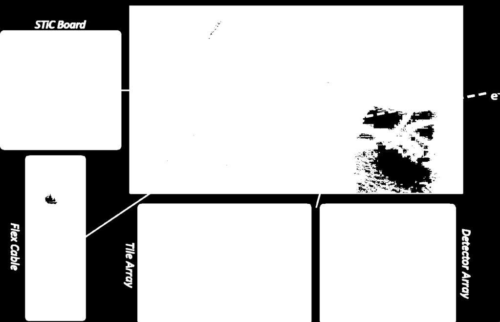
 4 MuTrig readout chips Scintillating fiber ribbons Silicon photo multiplier (SiPM) array")
21 Fiber Detector Fiber ribbon modules 32 mm wide ~290 mm long 4 layers fibers of 250 μm SiPM arrays (LHCb type) 4 MuTrig readout chips Scintillating fiber ribbons Silicon photo multiplier (SiPM) array 21
 4")

22 Fiber Detector Fiber ribbon modules 32 mm wide ~290 mm long 4 layers fibers of 250 μm SiPM arrays (LHCb type) 4 MuTRiG readout chips A demonstrator will be build by the end of the year Fiber tracker mechanical design study 22
23 Fiber Time Resolution Fiber detector prototypes tested Good time resolution: <400ps including ASIC 23

24 Tile Detector Submodule: In total 32 channel 3 x 3mm 2 SiPMs FEBA flex printed PCB MuTrig ASIC in BGA package Scintillator tiles Ej-228 o 6.5 x 6.5 x 5mm 3 o two types: center and edge ESR reflected foil, individual tile wrapping Rendering of Tile Detector sub module 24

25 Recurl station: Tile Detector 7 x 14 sub modules mounted on end rings and cooling structure Total length 368 cm 3136 channels Full detector phase I 2 recurl stations total of 6272 channels Rendering of Tile Detector station 25
 Excellent light yield Low crosstalk Prototype on cooling structure")
26 Tile Prototype Technical prototype build this year Develop assembly tools for mass production Tested with electron DESY (2-7 GeV) Excellent light yield Low crosstalk Prototype on cooling structure 26
 Excellent light yield Low crosstalk Tile sub-module prototype 27")
27 Tile Prototype Technical prototype build this year Develop assembly tools for mass production Tested with electron DESY (2-7 GeV) Excellent light yield Low crosstalk Tile sub-module prototype 27
28 Tile Prototype Tested with electron DESY (2-7 GeV) Excellent light yield Low crosstalk Excellent time resolution of 35 ps achieved o without time walk correction 28
29 Pixel Tracker Silicon pixel tracker: 2 vertex layers 2 outer layers o Central station o 2 recurl stations Total No of channels: Phase I M Mu3e detector scheme 29
30 Pixel Tracker Single layer structure: 50 µm silicon 25 µm Kapton flex print with aluminum traces 25 µm Kapton frame as support Less than 1 of radiation length per layer Helium cooling Total No of channels: Phase I M Pixel Tracker Rendering of CAD study 30
31 Pixel Tracker Successful feasibility studies for: Module mechanics He-cooling with low vibration Ultra-thin flexible circuit boards HV-CMOS small prototypes Readout board prototype Pixel Tracker Rendering of CAD study 31

32 Pixel Tracker Detailed design for: Module mechanics He-cooling distribution HV-CMOS large prototype Readout board pre production prototype Pixel Tracker Details of CAD 32

33 Pixel Tracker Detailed design for: Module mechanics He-cooling distribution HV-CMOS large prototype Readout board pre production prototype Pixel Tracker Details of CAD 33

34 Pixel Tracker Detailed design for: Module mechanics He-cooling distribution HV-CMOS large prototype Readout board pre production prototype Pixel Tracker Details of CAD 34

35 Pixel Tracker Detailed design for: Module mechanics He-cooling distribution HV-CMOS large prototype Readout board pre production prototype Pixel Tracker Details of CAD 35


36 Ultra-thin HDI Two layer HDI test design (top) Prototype from LTU Single point tape automated bonding 36
![Ultra-thin HDI Two layer HDI test design (top) Material Thickness [μm] X/X0 upper Al layer 14 1.](/docs-images/86/93155825/images/37-4.jpg "57 10 4 isolator (PI) 35 1.22 10 4 glue 10 0.25 10 4 lower Al layer 14 1.57 10 4 lower PI shield 10 0.")
37 Ultra-thin HDI Two layer HDI test design (top) Material Thickness [μm] X/X0 upper Al layer isolator (PI) glue lower Al layer lower PI shield total
38 HV-MAPS High Voltage Monolithic Active Pixel Sensors HV-CMOS technology N-well in p-substrate Reversely biased N well NMOS PMOS P substrate by Ivan Perić I. Perić, A novel monolithic pixelated particle detector implemented in highvoltage CMOS technology Nucl.Instrum.Meth., 2007, A582,


39 HV-MAPS High Voltage Monolithic Active Pixel Sensors HV-CMOS technology N-well in p-substrate Reversely biased ~85V o Depletion layer o Charge collection via drift Fast <1 ns charge collection o Thinning to 50 μm possible Integrated readout electronics -85V N well depletion layer P substrate ~9μm by Ivan Perić I. Perić, A novel monolithic pixelated particle detector implemented in highvoltage CMOS technology Nucl.Instrum.Meth., 2007, A582,
40 Full System on Chip 180 nm HV-CMOS Pixel matrix: o 128 x 200 pixels o 81 x 80 μm 2 each Analog part o Pixel sensor o Pre-amplifier Digital part o Comparator o Read out state machine o 1.25 Gbit/s serial data outputs Low power: o ~210mW/ cm 2 MuPix8 40

41 Sensor + Analog + Digital MuPix8 block diagram 41

42 MuPix8 Readout On Chip: Zero suppression Read-out state machine Voltage controlled oscillator + Phase locked loop Fast serializer 1.25 Gbit/s LVDS outputs Eye diagram MuPix8; eye height 199mV, eye width > 0.65 UI 42


43 Test beam measurements DESY test beam o 4 GeV electrons MuPix8 telescope o Beam telescope o 4 layers of MuPix8 pixel sensors o Includes DUT o Plastic scintillators as time reference MuPix8 beam telescope 43

44 Spatial Resolution Pixel size 80 μm x 81 μm Measured track residuals: o RMS y = 35 μm o 80 μm / 12 = 23 μm In Mu3e spatial resolution is dominated by multiple Coulomb scattering MuPix8 spatial resolution 44


45 Efficiencies >99.5% efficiency o 4 GeV DESY o 90 impact angle Low pixel noise o Rate per pixel ~0.2Hz MuPix8 Efficiency 45

46 and Noise >99.5% efficiency o 4 GeV DESY o 90 impact angle Low pixel noise o Rate per pixel ~0.2Hz o Hot pixels masked Noise map MuPix8 46

47 X-talk MUPIX8 DESY November 2017 o 4 GeV electrons@desy X-talk between o Rows o 10% around working point MuPix8 x-talk 47
48 Time Resolution Time difference of hits registered in MuPix8 and scintillator 4 GeV electrons Sampling rate is 125 MHz σ=21.67 ± 0.01 ns MuPix8 time resolution 48

49 Time Resolution Time difference of hits registered in MuPix8 and scintillator 4 GeV electrons Sampling rate is 125 MHz σ=14.48 ± 0.01 ns o After correcting for pixel to pixel delay differences MuPix8 time resolution pixel delay corrected 49
(90% CL) Two systems")

50 Summary Mu3e searches for lepton flavor violation > μ-decays BR O(10-15 )(90% CL) Two systems with excellent time resolution Ultra thin tracker with ~182M pixel Prototypes exceed requirements 50

51 Schedule 2019 Magnet delivery and detector construction 2020 Installation and commissioning at PSI 2021 Data taking at up to a few 10 8 μ/s 51

52 Outlook: Phase I performance Simulation 52

53 Outlook: Projected Sensitivity Single event sensitivity (SES) and the corresponding 90% and 95% C.L. upper limits versus data taking days for the Mu3e detector 53


54 Mu3e-: ETH Zürich, Switzerland PSI, Switzerland Institutes University of Geneva, Switzerland Physics Institute, University of Heidelberg, Germany Kirchhoff Institute, University of Heidelberg, Germany Institute for Process Data Processing and Electronics, Karlsruhe Institute of Technology, Germany Institute of Nuclear Physics, University of Mainz, Germany University of Zürich, Switzerland The University of Liverpool, United Kingdom University of Oxford, United Kingdom University of Bristol, United Kingdom University College London, United Kingdom 54
55 Acknowledgements The measurements leading to these results have been performed at the Test Beam Facility at DESY Hamburg (Germany), a member of the Helmholtz Association (HGF) We would like to thank PSI for valuable test beams! We thank the Institut für Kernphysik at the Johannes Gutenberg University Mainz for giving us the opportunity to take data at the MAMI beam. 55
56 Backup Slides 56
57 Challenges 57
58 Challenges High rates: 10 8 μ/s Good timing resolution: 100 ps Good vertex resolution: ~200 μm Excellent momentum resolution: ~ 0.5 MeV/c 2 Extremely low material budget: 1x10-3 X 0 (Si-Tracker Layer) HV-MAPS spectrometer 50 μm thin sensors B ~1 T field + Timing detectors 58
59 SciFi Backup 59
60 700 μm 433 μm staggered layers Details Thickness: theoretical ~ 683 mm measured ~ 750 mm < 1 g of glue / ribbon 254 μm 250 μm Horizontal gap between fibers ~ 4 μm Alternative: Square shape fibers 60


61 Fiber Winding Tool U channel 16 mm fiber ~ 40 cm More R&D to optimize the construction of the ribbons 61
62 Readout of Fibers Si-PMs (MPPCs) at both fiber ends SciFi column readout with Si-PM arrays LHCb type detector 64 channel monolithic device (custom design) ~250 µm effective pitch 50 µm 50 µm pixels Grouped in 0.25 mm 1 mm vertical columns Common bias voltage 62


63 Readout of Fibers Si-PMs (MPPCs) at both fiber ends SciFi column readout with Si-PM arrays LHCb type detector Reduced # of readout channels (2 64) Easy, direct coupling Higher occupancy Optical cross talk 63


64 SciFi Column Readout light travels preferentially in the cladding and exits the fiber at large angles optical cross talk between Si-PM columns 64

65 Readout Electronics MuTRiG ASIC (KIP) Fulfills SciFi requirements o Compact design Installation very close to Si-PM arrays o 32 channels 4 chips / Si-PM array Assuming MuTRiG can sustain ~10 MHz hitrate Performance to be tested o In particular for low photon yield STiC 65
66 Alternative Design with Square Fibers 2-3 layers of 250 mm square double cladding scint. fibers 128 fibers/layer Single fiber Al coating (minimum optical cross-talk) 16 mm 0.8 mm 66


67 Testing Square Fibers Fiber test setup developed at PSI timing performance 250 µm square fiber Cross talk: By sputtering 30 nm Al coating on the fiber cross talk < 1% was achieved 0.5 Nphe threshold σ = 750 ± 17 ps 67
68 Tile Detector Backup 68

69 Tile Time Resolution Coincidence between 2 tiles in a row Time resolution 70 ps Time-walk effect 14 ps 69


70 Efficiency Require hit in first & last column Look for hit in middle channel Efficiency > 99.5% eṯiles 70

71 Tile Detector Scintillating tiles 6.5 x 6.5 x 5.0 mm 3 7 Tile Modules per station o 448 tiles/module o Attached to end rings SiPMs attached to tiles o Distribution PCBs below o Readout through MuTRiG Tile detector 4 x 4 prototype 71
72 STiC Readout Developed at KIP for EndoTOFPET-US o Optimized for ToF applications Key features: o Digital timing & energy information STiC 2.0 o 64 channels (version 3.0) o 50 ps TDC bins o SiPM bias tuning o SiPM tail cancelation possibility (version 3.0) o Currently 1 MHz hit rate / chip o Up to 20 MHz in future version Version 2.0 successfully operated in test-beam STiC

 o Currently 1 MHz hit rate / chip o Up to 20 MHz in future version Version 2.")
73 STiC Readout Developed at KIP for EndoTOFPET-US o Optimized for ToF applications Key features: o Digital timing & energy information STiC 2.0 o 64 channels (version 3.0) o 50 ps TDC bins o SiPM bias tuning o SiPM tail cancelation possibility (version 3.0) o Currently 1 MHz hit rate / chip o Up to 20 MHz in future version Version 2.0 successfully operated in test-beam STiC

74 STiC Test Beam 74

75 STiC Test Beam 75

76 STiC Test Beam 76
77 HV-MAPS Backup 77
78 Prototype Overview Prototype Active Area Functionality Bugs Improvements MuPix mm 2 Sensor + analog Comparator ringing MuPix mm 2 Sensor + analog Temperature dependence First MuPix prototype No ringing MuPix mm 2 Sensor, analog, dig. MuPix4 9,42 mm 2 Sensor, analog, dig. bad pixel on/off, Zero time-stamp and row address for 50% of pixels First part of dig. readout Working digital readout, timestamp, temperature stable MuPix mm 2 Sensor, analog, dig.? Removed zero time-stamp and address bug MuPix mm 2 System on Chip X-talk Fast serial readout MuPix8 160 mm 2 Large S.o.C. First batch has metal 3 issues Large, Time walk correction 78

79 Full System on Chip 180 nm HV-CMOS Pixel matrix: o 40 x 32 pixels o 103 x 80 μm 2 each Analog part o Temperature tolerant Digital part o Full system on chip MuPix7 79


80 Sensor + Analog + Digital 80

81 Chip Readout On Chip: Zero suppression Read-out state machine PLL and VCO Fast serializer 1.25 Gbit/s LVDS output Eye diagram MuPix7; eye height > 130mV, eye width > 0.65 UI 81

82 Spatial Resolution Pixel size 80 μm x 103 μm Measured track residuals: o RMS x = 38.1 ± 0.1 μm o RMS y = 30.6 ± 0.1 μm 82
83 X-talk MUPIX7 PSI October 2015 o 250 MeV e + /µ + /pion X-talk between o Rows o Around 10% 83


84 X-talk MUPIX7 PSI October 2015 o 250 MeV e + /µ + /pion X-talk between o Rows Capacitive coupling o Line from diode to comparator o Strongly depends on layout 84


85 Efficiencies >99.5% efficiency o 4 GeV electrons@desy o 90 impact angle o Individual pixel thresholds MuPix7 Efficiency 85


86 Efficiencies rotated Sensor >99.8% efficiency o 4 GeV electrons o 30 impact angle o Individual pixel thresholds e + MUPIX7 MuPix7 under angle MuPix7 Efficiency 86

87 Time Stamps Time difference of hits registered in MuPix 7 and scintillator 4 GeV electrons Sampling rate is 62.5 MHz Time Resolution of Pixels 87

88 Thinned Sensors Prototypes thinned: o MuPix7 thinned to 50, 62, 75μm Good performance of thin chips o In lab o In particle beam MuPix4 thinned to 50μm 88

89 Setup March 2016 DESY Beam-line TB22 o up to 5 GeV electrons Aconite telescope MuPix7 prototype Readout setup from PI Heidelberg DESY test-beam in EUDET telescope 89

90 Sub-Pixel Efficiencies Hit efficiency map and projections for 2 2 pixel array 4 GeV electrons Bias voltage 40V to enhance the inefficient regions 90
91 Temperature Dependence Pulse shape vs temperature o Injection pulse to pixel discriminator output Climate chamber o 0 C, 20 C, 40 C, 60 C Significant change to Pulse shape Signal amplitude Slight change to time resolution Re-calibration MUPIX7 High bias currents (1W/cm 2 ) HV -85V 91


92 Temperature Dependence Pulse shape vs temperature o Injection pulse to pixel discriminator output Climate chamber o 0 C, 20 C, 40 C, 60 C Significant change to Pulse shape Signal amplitude Slight change to time resolution Re-calibration 92
93 Mechanics Backup 93
94 Mu3e Silicon Detector Conical target Inner double layer o 8 and 10 sides of 2 x 12 cm 2 Outer double layer o 24 and 28 sides of 2 x 36 cm 2 Re-curl layers o 24 and 28 sides of 2x 36 cm 2 o Both sides 94
95 Mu3e Silicon Detector Conical target Inner double layer o 8 and 10 sides of 2 x 12 cm 2 Outer double layer o 24 and 28 sides of 2 x 36 cm 2 Re-curl layers o 24 and 28 sides of 2x 36 cm 2 o Both sides 95
96 Mu3e Silicon Detector Conical target Inner double layer o 8 and 10 sides of 2 x 12 cm 2 Outer double layer o 24 and 28 sides of 2 x 36 cm 2 Re-curl layers o 24 and 28 sides of 2x 36 cm 2 o Both sides 96
97 Mu3e Silicon Detector Conical target Inner double layer o 8 and 10 sides of 2 x 12 cm 2 Outer double layer o 24 and 28 sides of 2 x 36 cm 2 Re-curl layers o 24 and 28 sides of 2 x 36 cm 2 o Both sides 108 inner sensors 2736 outer sensors ~ pixel 97


98 Sandwich Design HV-MAPS o Thinned to 50 μm o Sensors 2 x 2 cm 2 Kapton flex print o 25 μm Kapton o 14 μm Alu traces Kapton Frame Modules o 25 μm foil o Self supporting Alu end wheels o Support for all detectors 0.11% of X 0 98

99 Thinned Pixel Sensors HV-MAPS* o Thinned to 50 μm o Sensors 2 x 2 cm 2 Kapton flex print o 25 μm Kapton o 14 μm Alu traces Kapton Frame Modules o 25 μm foil o Self supporting Alu end wheels o Support for all detectors MuPix3 thinned to < 90μm 99
100 Kapton Flex Print HV-MAPS o Thinned to 50 μm o Sensors 2 x 2 cm 2 Kapton flex print o 25 μm Kapton o 14 μm Alu traces Kapton Frame Modules o 25 μm foil o Self supporting Alu end wheels o Support for all detectors Laser-cut flex print prototype 100

101 Pixel Modules HV-MAPS o Thinned to 50 μm o Sensors 2 x 2 cm 2 Kapton flex print o 25 μm Kapton o 14 μm Alu traces Kapton Frame Modules o 25 μm foil o Self supporting Alu end wheels o Support for all detectors CAD of Kapton frames 101

102 Overall Design HV-MAPS o Thinned to 50 μm o Sensors 2 x 2 cm 2 Kapton flex print o 25 μm Kapton o 14 μm Alu traces Kapton Frame Modules o 25 μm foil o Self supporting Alu end wheels o Support for all detectors Two halves for layers modules in layer 3 7 modules in layer 4 CAD of Kapton frames 102

103 Inner Layers HV-MAPS o Thinned to 50 μm o Sensors 2 x 2 cm 2 Kapton flex print o 25 μm Kapton o 14 μm Alu traces Kapton Frame Modules o 25 μm foil o Self supporting Alu end wheels o Support for all detectors Rendering of vertex detector CAD 103

104 Outer Module HV-MAPS o Thinned to 50 μm o Sensors 2 x 2 cm 2 Kapton flex print o 25 μm Kapton o 14 μm Alu traces Kapton Frame Modules o 25 μm foil o Self supporting Alu end wheels o Support for all detectors Layer 3 Prototype in Assembling Frame with 50 μm Glass 104

105 Detector Frame HV-MAPS o Thinned to 50 μm o Sensors 2 x 2 cm 2 Kapton flex print o 25 μm Kapton o 14 μm Alu traces Kapton Frame Modules o 25 μm foil o Self supporting Alu end wheels o Support for all detectors Pixel detector CAD rendering 105


106 Thinning 50 μm Si-wafers o Commercially available o HV-CMOS 50 μm (AMS) o 50 μm for MuPix4 and MuPix7 106
107 DAQ Backup 107

108 Trigger-less DAQ Front end links o Pixel sensor to on-detector FPGA 1250 Mbit/s LVDS o Timing detector readout Optical links from detector o Front end FPGAs o to switching boards o 6.4 Gbit/s Optical links in counting room o Off-detector read out boards o to PC Farm Pixel Sensor Silicon FPGAs x86 Switching board x2 PC x12 108
109 Trigger-less DAQ Front end links o Pixel sensor to on-detector FPGA 1250 Mbit/s LVDS o Timing detector readout Optical links from detector o Front end FPGAs o to switching boards o 6.4 Gbit/s Optical links in counting room o Off-detector read out boards o to PC Farm O(Tbit/s) Pixel Pixel Sensor Pixel Sensor Pixel Sensor Sensor Silicon FPGAs x86 Switching board x2 Fiber Fiber Fiber Fiber Fiber FPGAs 12x Tile Tile Tile Tile x2844 x192 x196 Switching board x1 PC x12 Tile FPGAs x14 Switching board x1 109
110 Front End FPGAs FPGAs in magnet volume o 112 pieces Receive sensor data o LVDS inputs 6.4 Gbit/s outputs o 8 optical links o to counting house 1250 Mbit/s LVDS in x Gbit/s optical Pixel Sensor Front end FPGA Switching board 110


111 Tasks, problems, challenges Hard-, firm- and software developments Testing custom designed front-end boards and bringing them to operation Data transmission studies o Electrical links o Optical links Data reduction at front-end: Up to Gbps 1 6 Gbps with as little logic utilization as possible 111

112 Front End Board V1.02 Bug-fix of Front End Board V1.0 o Extra resistors o Extra voltage regulator DC-DC for entire partition Eight PCBs produced o Tested and ok DC-DC on FEB 112


113 Front End Board V2.0 Better FPGA FireFly optical transceivers o Replace MiniPods and QSFP with 2x Samtec FireFly 4-fold optical transceiver o Smaller, cheaper, o Performance currently under evaluation (B.Sc. Thesis Benjamin Weinlaeder) 113
114 Trigger-less DAQ Front end links o Pixel sensor to on-detector FPGA 1250 Mbit/s LVDS o Timing detector readout Optical links from detector o Front end FPGAs o to readout boards o 6.4 Gbit/s Optical links in counting room o Off-detector read out boards o to PC Farm O(Tbit/s) Pixel Pixel Sensor Pixel Sensor Pixel Sensor Sensor Silicon FPGAs x86 Switching board x2 Fiber Fiber Fiber Fiber Fiber FPGAs x12 Switching board x1 PC x12 Tile Tile Tile Tile Tile FPGAs x14 Switching board x1 114


115 Trigger-less DAQ Front end links o Pixel sensor to on-detector FPGA 1250 Mbit/s LVDS o Timing detector readout Optical links from detector o Front end FPGAs o to switching boards o 6.4 Gbit/s Optical links in counting room o Off-detector read out boards o to PC Farm 6.4 Gbit/s Pixel Pixel Sensor Pixel Sensor Pixel Sensor Sensor Silicon FPGAs x86 Switching board x2 Fiber Fiber Fiber Fiber Fiber FPGAs x12 Readout board x2 PC x12 Tile Tile Tile Tile Tile FPGAs x14 Readout board x2 115
116 Switching Board FPGA switching boards o per sub-detector 6.4 Gbit/s optical inputs o inputs 10 Gbit/s optical output o 12 outputs to PCs Switching network o One output per PC Front Front Front end Front end end end FPGA FPGA FPGA 6.4 Gbit/s Optical x48 10 Gbit/s Optical Switching board x12 PC PC PC 116
117 Switching Board FPGA switching boards o 4 per sub-detector 6.4 Gbit/s optical inputs o inputs 10 Gbit/s optical output o 12 outputs to PCs Switching network o One output per PC Front Front Front end Front end end end FPGA FPGA FPGA 6.4 Gbit/s Optical 10 Gbit/s Optical Switching board x12 PC PC PC 117

118 Switching Board PCIe40 Developed for LHCb and ALICE upgrade by CPPM (Marseille) 48 optical I/Os Optcial network switch fro Mu3e filter farm Mu3e will receive samples from the current production 118
119 Trigger-less DAQ Front end links o Pixel sensor to on-detector FPGA 1250 Mbit/s LVDS o Timing detector readout Optical links from detector o Front end FPGAs o to readout boards o 6.4 Gbit/s Optical links in counting room o Off-detector read out boards o to PC Farm O(Tbit/s) Pixel Pixel Sensor Pixel Sensor Pixel Sensor Sensor Silicon FPGAs x86 Switching board x4 x48 Fiber Fiber Fiber Fiber Fiber FPGAs x12 Switching board x2 x24 PCs Tile Tile Tile Tile x24 Tile FPGAs x14 Switching board x2 119

120 GPU-PC PC with GPU 10 Gbit/s Fiber input o 8 inputs from sub-detectors Data filtering o Timing Filter on FPGA o Track filter on GPU o Data to tape < 100 MB/s GPU computer 120

121 GPU-PC PC with GPU 10 Gbit/s Fiber input o 8 inputs from sub-detectors Data filtering o Timing Filter on FPGA o Track filter on GPU o Data to tape < 100 MB/s FPGA PCIe board GPU computer 121
122 Receiving FPGA board PC side De5a-NET boards from Terasic Successfully tested at Mainz 8 out of 12 boards already acquired 122
123 DAQ tests Backup 123


124 Front End Board V2.0 Better FPGA o ArriaV instead of StratixIV o Lower power consumption 6.6W 3.3W (<10W) FireFly optical transceivers o 2 x 1W Clock distribution chips o SI x 1W DC-DC only for FEB o FEAST2MD compatible o Or based on TI chip set i.e. LM
125 Readout Vertical Slice Test Pixel detector o HV-MAPS (MuPix8) Large prototype Front end board Pixel Pixel Fiber Tile Sensor Pixel Fiber Tile Sensor Pixel Fiber Tile Tile Sensor MuPix MuTRiG MuTRiG FE-PCB FE-PCB FE-PCB Switching board PC o PCIe40 o Delivery 2018 Switching board PCs Switching board Switching board 125
 Large prototype Front end board Pixel Pixel")


126 Readout Vertical Slice Test Pixel detector o HV-MAPS (MuPix8) Large prototype Front end board Pixel Pixel Fiber Tile Sensor Pixel Fiber Tile Sensor Pixel Fiber Tile Tile Sensor MuPix MuTRiG MuTRiG FE-PCB FE-PCB FE-PCB Switching board PC o PCIe40 o Delivery 2018 Switching board PCs Switching board Switching board 126


127 Optical cabling scheme 127
128 Backup Area Planning 128


129 PSI μ-beam Paul Scherrer Institute Switzerland: 2.2 ma of 590 MeV/c protons Surface muons from target E Up to ~10 8 μ/s >10 15 muon decays per year 129

130 Area Planning Good progress in terms of CAD, civil engineering for: Platforms Access ways Counting containers Power Cooling Remark: Space in area extremely limited 130

131 Area Planning Good progress in terms of CAD, civil engineering for: Platforms Access ways Counting containers Power Cooling Remark: Space in area extremely limited 131

132 Area Planning Good progress in terms of CAD, civil engineering for: Platforms Access ways Counting containers Power Cooling Remark: Space in area extremely limited 132
133 Area Planning Good progress in terms of CAD, civil engineering for: Platforms Access ways Counting containers Power Cooling Remark: Space in area extremely limited 133
134 PSI μ-beam Paul Scherrer Institute Switzerland: 2.2 ma of 590 MeV/c protons Surface muons from target E Up to ~10 8 μ/s >10 15 muon decays per year O(10 8 µ/s) 134


135 Area Layout Modified separator frame 135
136 Cooling Backup 136


137 Simulation He cooling 400mW/cm 2 137

138 Test Results 1:1 Prototype o Layer 3+4 of silicon tracker o Ohmic heating 400mW/cm 2 Cooling He o at several m/s Temperature sensors attached to foil o LabVIEW readout Results promising o ΔT < 60 K No sign of vibration in air 138


139 Cooling Concept Liquid cooling o Timing detectors o Front end boards o DC-DC boards o Wiener LV crates o Filter farm racks Gaseous He cooling o For Silicon tracker o General cooling inside magnet Tile cooling simulation 139
140 He Cooling Gaseous He cooling o Low multiple Coulomb scattering o He more effective than air Global flow inside Magnet volume Local flow for Tracker o V-shapes o Outer surface In between layers Between SciFi and layers He He 400mW/cm 2 x 11376cm 2 = KW 140
141 Pixel helium cooling BVR49 141
142 Pixel helium cooling BVR49 Multiple He cooling circuits Volumetric flow between o 0.72 m 3 /min. and o 23 m 3 /min. Separately fine adjustable Segment overall He system? o Introduce redundancy 142

143 He cooling requirements Cooling power o Pixel power dissipation 4.55kW o Enough reserve Up to 50 m 3 /min. Reliable start up procedure Reliable emergency reaction Good temperature stability Dry and clean He recovery system 143


144 He cooling system Water cooler He buffer Pump Heat exchanger Control & Quality monitor He recovery Mu3e Detector 144

145 Water cooler 10kW chiller in HD o Commissioned 2016 o Massive 2.25kW chiller in HD o Borrowed from H1 o Commissioned in 2016 o Intermediate size Extra chiller required? Copyright Parker 145

146 Heat exchanger 10kW heat exchanger in HD Water to He Industry standard 146

147 Helium buffer Large He buffer Over pressurized Store cold He Eliminate vibrations from pumps Delivers He in case pump stops 147
148 He recovery He in closed system Drying system Remove other gases o Membrane filter o Very efficient for air/he separation Membrane 148

149 Control and quality monitor Slow control system for Monitoring o Pumps o Chillers o Valves Safety system o Shutdown o Humidity o Temperatures o Pressures o Flows o Humidity o Contaminations 149

150 Piping Volumetric flow high o 50m 3 /min. 20cm diameter pipes Insulated Flexible (?) 150

151 Pump(s) Large throughput o Up to 50m 3 /min. Little overpressure o 500 mbar ok Must run constantly Must not contaminate the He Contact air conditioning experts? 151

152 Installation space System of very large devices Vibrations from o Pumps o Chillers Large pipes 152

153 Summary He cooling system is: o Large o Complex o Safety relevant Chillers and He heat exchanger in HD Pumps, pipes, valves, recovery system and control system to be acquired/designed 153
154 He Properties Molecular weight : g/mol Gaseous phase Gas density (1.013 bar at boiling point) : kg/m 3 Gas density (1.013 bar and 15 C (59 F)) : kg/m 3 Compressibility Factor (Z) (1.013 bar and 15 C (59 F)) : Specific gravity : Specific volume (1.013 bar and 25 C (77 F)) : m 3 /kg Heat capacity at constant pressure (Cp) (1.013 bar and 25 C (77 F)) : kj/(mol.k) Heat capacity at constant volume (Cv) (1.013 bar and 25 C (77 F)) : kj/(mol.k) Ratio of specific heats (Gamma:Cp/Cv) (1.013 bar and 25 C (77 F)) : Viscosity (1.013 bar and 0 C (32 F)) : E -04 Poise Thermal conductivity (1.013 bar and 0 C (32 F)) : mw/(m.k) 154
155 Air Properties Molecular weight : g/mol Gaseous phase Gas density (1.013 bar at boiling point) : 3.2 kg/m 3 Gas density (1.013 bar and 15 C (59 F)) : kg/m 3 Compressibility Factor (Z) (1.013 bar and 15 C (59 F)) : Specific gravity : 1 Specific volume (1.013 bar and 25 C (77 F)) : m 3 /kg Heat capacity at constant pressure (Cp) (1.013 bar and 25 C (77 F)) : kj/(mol.k) Heat capacity at constant volume (Cv) (1.013 bar and 25 C (77 F)) : kj/(mol.k) Ratio of specific heats (Gamma:Cp/Cv) (1.013 bar and 25 C (77 F)) : Viscosity (1 bar and 0 C (32 F)) : 1.721E -04 Poise Thermal conductivity (1.013 bar and 0 C (32 F)) : mw/(m.k) 155

156 Liquid Cooling Beam pipe cooling o With cooling liquid o 5 C temperature o Significant flow possible o using grooves in pipe For electronics o FPGAs and o Power regulators o Mounted to cooling plates Total power several kw Old design study 156

157 He Cooling Gaseous He cooling o Low multiple Coulomb scattering o He more effective than air Global flow inside Magnet volume Local flow for Tracker o Distribution to Frame V-shapes Outer surface Temperatures between 20 C to 70 C ok. 157

158 He Cooling Gaseous He cooling o Low multiple Coulomb scattering o He more effective than air Global flow inside Magnet volume Local flow for Tracker o Distribution to Frame V-shapes Outer surface Old design study 158


159 He Cooling Gaseous He cooling o Low multiple Coulomb scattering o He more effective than air Global flow inside Magnet volume Local flow for Tracker o Distribution to Frame V-shapes Outer surface Old design study 159

160 He Cooling Gaseous He cooling o Low multiple Coulomb scattering o He more effective than air Global flow inside Magnet volume Distribution in Frame Local flow: V-shapes Gap flow: Outer surface 400mW/cm 2 x 11664cm KW 160
161 He Cooling Gaseous He cooling o Low multiple Coulomb scattering o He more effective than air Global flow inside Magnet volume Local flow for Tracker o Distribution to Frame V-shapes Outer surface Kapton Frame Cooling outlets V-shape Old design study 161

162 He Cooling Gaseous He cooling o Low multiple Coulomb scattering o He more effective than air Global flow inside Magnet volume Local flow for Tracker o Distribution to Frame V-shapes Outer surface Old design study 162

163 Tests Full scale prototype o Layer 3+4 of silicon tracker o Ohmic heating (150mW/cm 2 ) o W for layer 3 +4 o of Aluminum-Kapton Cooling with external fan o Air at several m/s Temperature sensors attached to foil o LabView readout First results promising o ΔT < 60 K 163

164 164

165 Tests Full scale prototype o Layer 3+4 of silicon tracker o Ohmic heating (150mW/cm 2 ) o W for layer 3 +4 o of Aluminum-Kapton Cooling with external fan o Air at several m/s Temperature sensors attached to foil o LabView readout First results promising o ΔT < 60 K 165

166 Test Results Full scale prototype o Layer 3+4 of silicon tracker o Ohmic heating (150mW/cm 2 ) o W for layer 3 +4 o of Aluminum-Kapton Cooling with external fan o Air at several m/s Temperature sensors attached to foil o LabView readout First results promising o ΔT < 60 K No sign of vibration in air 166

167 Comparison Simulation and Tests 167


168 Comparison Simulation He and Air He Air v = 4.0 m s 168
169 He Cooling 750 mw/cm 2 169
Novel thin High Voltage Monolithic Active Pixel Sensors for the Mu3e experiment
 Novel thin High Voltage Monolithic Active Pixel Sensors for the Mu3e experiment Dirk Wiedner, Heidelberg On Behalf of the Mu3e Collaboration 1 The Mu3e Signal μ + e + e - e + rare in νsm o Branching ratio
HV-MAPS. Dirk Wiedner Physikalisches Institut der Universität Heidelberg on behalf of the Mu3e silicon detector collaboration
 HV-MAPS Dirk Wiedner Physikalisches Institut der Universität Heidelberg on behalf of the Mu3e silicon detector collaboration 1 From Tracking to Pixel Sensors 2 Decay point o Primary vertex: o Tracks of
The High-Voltage Monolithic Active Pixel Sensor for the Mu3e Experiment
 The High-Voltage Monolithic Active Pixel Sensor for the Mu3e Experiment Shruti Shrestha On Behalf of the Mu3e Collaboration International Conference on Technology and Instrumentation in Particle Physics
CMOS Detectors Ingeniously Simple!
 CMOS Detectors Ingeniously Simple! A.Schöning University Heidelberg B-Workshop Neckarzimmern 18.-20.2.2015 1 Detector System on Chip? 2 ATLAS Pixel Module 3 ATLAS Pixel Module MCC sensor FE-Chip FE-Chip
KLauS4: A Multi-Channel SiPM Charge Readout ASIC in 0.18 µm UMC CMOS Technology
 1 KLauS: A Multi-Channel SiPM Charge Readout ASIC in 0.18 µm UMC CMOS Technology Z. Yuan, K. Briggl, H. Chen, Y. Munwes, W. Shen, V. Stankova, and H.-C. Schultz-Coulon Kirchhoff Institut für Physik, Heidelberg
CALICE AHCAL overview
 International Workshop on the High Energy Circular Electron-Positron Collider in 2018 CALICE AHCAL overview Yong Liu (IHEP), on behalf of the CALICE collaboration Nov. 13, 2018 CALICE-AHCAL Progress, CEPC
Track and Vertex Reconstruction on GPUs for the Mu3e Experiment
 Track and Vertex Reconstruction on GPUs for the Mu3e Experiment Dorothea vom Bruch for the Mu3e Collaboration GPU Computing in High Energy Physics, Pisa September 11th, 2014 Physikalisches Institut Heidelberg
PoS(VERTEX2015)008. The LHCb VELO upgrade. Sophie Elizabeth Richards. University of Bristol
008. The LHCb VELO upgrade. Sophie Elizabeth Richards. University of Bristol") University of Bristol E-mail: sophie.richards@bristol.ac.uk The upgrade of the LHCb experiment is planned for beginning of 2019 unitl the end of 2020. It will transform the experiment to a trigger-less
University of Bristol E-mail: sophie.richards@bristol.ac.uk The upgrade of the LHCb experiment is planned for beginning of 2019 unitl the end of 2020. It will transform the experiment to a trigger-less
Strip Detectors. Principal: Silicon strip detector. Ingrid--MariaGregor,SemiconductorsasParticleDetectors. metallization (Al) p +--strips
 p +--strips") Strip Detectors First detector devices using the lithographic capabilities of microelectronics First Silicon detectors -- > strip detectors Can be found in all high energy physics experiments of the last
Strip Detectors First detector devices using the lithographic capabilities of microelectronics First Silicon detectors -- > strip detectors Can be found in all high energy physics experiments of the last
Track Triggers for ATLAS
 Track Triggers for ATLAS André Schöning University Heidelberg 10. Terascale Detector Workshop DESY 10.-13. April 2017 from https://www.enterprisedb.com/blog/3-ways-reduce-it-complexitydigital-transformation
ITk silicon strips detector test beam at DESY
 ITk silicon strips detector test beam at DESY Lucrezia Stella Bruni Nikhef Nikhef ATLAS outing 29/05/2015 L. S. Bruni - Nikhef 1 / 11 Qualification task I Participation at the ITk silicon strip test beams
The LHCb VELO Upgrade. Stefano de Capua on behalf of the LHCb VELO group
 The LHCb VELO Upgrade Stefano de Capua on behalf of the LHCb VELO group Overview [J. Instrum. 3 (2008) S08005] LHCb / Current VELO / VELO Upgrade Posters M. Artuso: The Silicon Micro-strip Upstream Tracker
Towards a 10 μs, thin high resolution pixelated CMOS sensor system for future vertex detectors
 Towards a 10 μs, thin high resolution pixelated CMOS sensor system for future vertex detectors Rita De Masi IPHC-Strasbourg On behalf of the IPHC-IRFU collaboration Physics motivations. Principle of operation
High granularity scintillating fiber trackers based on Silicon Photomultiplier
 High granularity scintillating fiber trackers based on Silicon Photomultiplier A. Papa Paul Scherrer Institut, Villigen, Switzerland E-mail: angela.papa@psi.ch Istituto Nazionale di Fisica Nucleare Sez.
Pixel characterization for the ITS/MFT upgrade. Audrey Francisco
 Pixel characterization for the ITS/MFT upgrade Audrey Francisco QGP France, Etretat, 14/10/2015 Outline 1 The MFT upgrade 2 Pixel sensor Technology choice Full scale prototypes 3 Characterization campaign
arxiv: v1 [physics.ins-det] 26 Nov 2015
![arxiv: v1 [physics.ins-det] 26 Nov 2015](/thumbs/91/104762493.jpg "arxiv: v1 [physics.ins-det] 26 Nov 2015") arxiv:1511.08368v1 [physics.ins-det] 26 Nov 2015 European Organization for Nuclear Research (CERN), Switzerland and Utrecht University, Netherlands E-mail: monika.kofarago@cern.ch The upgrade of the Inner
arxiv:1511.08368v1 [physics.ins-det] 26 Nov 2015 European Organization for Nuclear Research (CERN), Switzerland and Utrecht University, Netherlands E-mail: monika.kofarago@cern.ch The upgrade of the Inner
Pixel hybrid photon detectors
 Pixel hybrid photon detectors for the LHCb-RICH system Ken Wyllie On behalf of the LHCb-RICH group CERN, Geneva, Switzerland 1 Outline of the talk Introduction The LHCb detector The RICH 2 counter Overall
EUDET Pixel Telescope Copies
 EUDET Pixel Telescope Copies Ingrid-Maria Gregor, DESY December 18, 2010 Abstract A high resolution beam telescope ( 3µm) based on monolithic active pixel sensors was developed within the EUDET collaboration.
Test Beam Measurements for the Upgrade of the CMS Phase I Pixel Detector
 Test Beam Measurements for the Upgrade of the CMS Phase I Pixel Detector Simon Spannagel on behalf of the CMS Collaboration 4th Beam Telescopes and Test Beams Workshop February 4, 2016, Paris/Orsay, France
Status of the LHCb Experiment
 Status of the LHCb Experiment Werner Witzeling CERN, Geneva, Switzerland On behalf of the LHCb Collaboration Introduction The LHCb experiment aims to investigate CP violation in the B meson decays at LHC
CMS Tracker Upgrades. R&D Plans, Present Status and Perspectives. Benedikt Vormwald Hamburg University on behalf of the CMS collaboration
 R&D Plans, Present Status and Perspectives Benedikt Vormwald Hamburg University on behalf of the CMS collaboration EPS-HEP 2015 Vienna, 22.-29.07.2015 CMS Tracker Upgrade Program LHC HL-LHC ECM[TeV] 7-8
The LHCb Upgrade BEACH Simon Akar on behalf of the LHCb collaboration
 The LHCb Upgrade BEACH 2014 XI International Conference on Hyperons, Charm and Beauty Hadrons! University of Birmingham, UK 21-26 July 2014 Simon Akar on behalf of the LHCb collaboration Outline The LHCb
The MUSE experiment. Technical Overview. Guy Ron (for the MUSE collaboration) Hebrew University of Jerusalem
 Hebrew University of Jerusalem") The MUSE experiment Technical Overview Guy Ron (for the MUSE collaboration) Hebrew University of Jerusalem MUSE is not your garden variety scattering experiment Low beam flux Large angle, non-magnetic
The MUSE experiment Technical Overview Guy Ron (for the MUSE collaboration) Hebrew University of Jerusalem MUSE is not your garden variety scattering experiment Low beam flux Large angle, non-magnetic
Beam Condition Monitors and a Luminometer Based on Diamond Sensors
 Beam Condition Monitors and a Luminometer Based on Diamond Sensors Wolfgang Lange, DESY Zeuthen and CMS BRIL group Beam Condition Monitors and a Luminometer Based on Diamond Sensors INSTR14 in Novosibirsk,
The VELO Upgrade. Eddy Jans, a (on behalf of the LHCb VELO Upgrade group) a
 a") The VELO Upgrade Eddy Jans, a (on behalf of the LHCb VELO Upgrade group) a Nikhef, Science Park 105, 1098 XG Amsterdam, The Netherlands E-mail: e.jans@nikhef.nl ABSTRACT: A significant upgrade of the LHCb
The VELO Upgrade Eddy Jans, a (on behalf of the LHCb VELO Upgrade group) a Nikhef, Science Park 105, 1098 XG Amsterdam, The Netherlands E-mail: e.jans@nikhef.nl ABSTRACT: A significant upgrade of the LHCb
A new single channel readout for a hadronic calorimeter for ILC
 A new single channel readout for a hadronic calorimeter for ILC Peter Buhmann, Erika Garutti,, Michael Matysek, Marco Ramilli for the CALICE collaboration University of Hamburg E-mail: sebastian.laurien@desy.de
Pixel sensors with different pitch layouts for ATLAS Phase-II upgrade
 Pixel sensors with different pitch layouts for ATLAS Phase-II upgrade Different pitch layouts are considered for the pixel detector being designed for the ATLAS upgraded tracking system which will be operating
 http://clicdp.cern.ch Hybrid Pixel Detectors with Active-Edge Sensors for the CLIC Vertex Detector Simon Spannagel on behalf of the CLICdp Collaboration Experimental Conditions at CLIC CLIC beam structure
Thin Silicon R&D for LC applications
 Thin Silicon R&D for LC applications D. Bortoletto Purdue University Status report Hybrid Pixel Detectors for LC Next Linear Collider:Physic requirements Vertexing 10 µ mgev σ r φ,z(ip ) 5µ m 3 / 2 p sin
Phase 1 upgrade of the CMS pixel detector
 Phase 1 upgrade of the CMS pixel detector, INFN & University of Perugia, On behalf of the CMS Collaboration. IPRD conference, Siena, Italy. Oct 05, 2016 1 Outline The performance of the present CMS pixel
LHCb Preshower(PS) and Scintillating Pad Detector (SPD): commissioning, calibration, and monitoring
 and Scintillating Pad Detector (SPD): commissioning, calibration, and monitoring") LHCb Preshower(PS) and Scintillating Pad Detector (SPD): commissioning, calibration, and monitoring Eduardo Picatoste Olloqui on behalf of the LHCb Collaboration Universitat de Barcelona, Facultat de Física,
LHCb Preshower(PS) and Scintillating Pad Detector (SPD): commissioning, calibration, and monitoring Eduardo Picatoste Olloqui on behalf of the LHCb Collaboration Universitat de Barcelona, Facultat de Física,
The CMS Outer HCAL SiPM Upgrade.
 The CMS Outer HCAL SiPM Upgrade. Artur Lobanov on behalf of the CMS collaboration DESY Hamburg CALOR 2014, Gießen, 7th April 2014 Outline > CMS Hadron Outer Calorimeter > Commissioning > Cosmic data Artur
Construction of the silicon tracker for the R3B experiment.
 Construction of the silicon tracker for the R3B experiment. M.Borri (STFC) on behalf of the teams at Daresbury Laboratory, Edinburgh and Liverpool Universities. Outline: FAIR and R3B. Overview of Si tracker.
Production of HPDs for the LHCb RICH Detectors
 Production of HPDs for the LHCb RICH Detectors LHCb RICH Detectors Hybrid Photon Detector Production Photo Detector Test Facilities Test Results Conclusions IEEE Nuclear Science Symposium Wyndham, 24 th
Pixel detector development for the PANDA MVD
 Pixel detector development for the PANDA MVD D. Calvo INFN - Torino on behalf of the PANDA MVD group 532. WE-Heraeus-Seminar on Development of High_Resolution Pixel Detectors and their Use in Science and
Contents. The AMADEUS experiment at the DAFNE collider. The AMADEUS trigger. SiPM characterization and lab tests
 Contents The AMADEUS experiment at the DAFNE collider The AMADEUS trigger SiPM characterization and lab tests First trigger prototype; tests at the DAFNE beam Second prototype and tests at PSI beam Conclusions
The PERDaix Detector. Thomas Kirn I. Physikalisches Institut B. July 5 th 2011, 6 th International Conference on New Developments In Photodetection
 Proton Electron Radiation Detector Aix la Chapelle The PERDaix Detector Thomas Kirn I. Physikalisches Institut B July 5 th 2011, 6 th International Conference on New Developments In Photodetection Motivation
Results of FE65-P2 Pixel Readout Test Chip for High Luminosity LHC Upgrades
 for High Luminosity LHC Upgrades R. Carney, K. Dunne, *, D. Gnani, T. Heim, V. Wallangen Lawrence Berkeley National Lab., Berkeley, USA e-mail: mgarcia-sciveres@lbl.gov A. Mekkaoui Fermilab, Batavia, USA
Development of Telescope Readout System based on FELIX for Testbeam Experiments
 Development of Telescope Readout System based on FELIX for Testbeam Experiments, Hucheng Chen, Kai Chen, Francessco Lanni, Hongbin Liu, Lailin Xu Brookhaven National Laboratory E-mail: weihaowu@bnl.gov,
A new strips tracker for the upgraded ATLAS ITk detector
 A new strips tracker for the upgraded ATLAS ITk detector, on behalf of the ATLAS Collaboration : 11th International Conference on Position Sensitive Detectors 3-7 The Open University, Milton Keynes, UK.
The Compact Muon Solenoid Experiment. Conference Report. Mailing address: CMS CERN, CH-1211 GENEVA 23, Switzerland
 Available on CMS information server CMS CR -2017/349 The Compact Muon Solenoid Experiment Conference Report Mailing address: CMS CERN, CH-1211 GENEVA 23, Switzerland 09 October 2017 (v4, 10 October 2017)
Development of Pixel Detectors for the Inner Tracker Upgrade of the ATLAS Experiment
 Development of Pixel Detectors for the Inner Tracker Upgrade of the ATLAS Experiment Natascha Savić L. Bergbreiter, J. Breuer, A. Macchiolo, R. Nisius, S. Terzo IMPRS, Munich # 29.5.215 Franz Dinkelacker
A Prototype Amplifier-Discriminator Chip for the GLAST Silicon-Strip Tracker
 A Prototype Amplifier-Discriminator Chip for the GLAST Silicon-Strip Tracker Robert P. Johnson Pavel Poplevin Hartmut Sadrozinski Ned Spencer Santa Cruz Institute for Particle Physics The GLAST Project
on-chip Design for LAr Front-end Readout
 Silicon-on on-sapphire (SOS) Technology and the Link-on on-chip Design for LAr Front-end Readout Ping Gui, Jingbo Ye, Ryszard Stroynowski Department of Electrical Engineering Physics Department Southern
Preparing for the Future: Upgrades of the CMS Pixel Detector
 : KSETA Plenary Workshop, Durbach, KIT Die Forschungsuniversität in der Helmholtz-Gemeinschaft www.kit.edu Large Hadron Collider at CERN Since 2015: proton proton collisions @ 13 TeV Four experiments:
Muon detection in security applications and monolithic active pixel sensors
 Muon detection in security applications and monolithic active pixel sensors Tracking in particle physics Gaseous detectors Silicon strips Silicon pixels Monolithic active pixel sensors Cosmic Muon tomography
The CMS Silicon Strip Tracker and its Electronic Readout
 The CMS Silicon Strip Tracker and its Electronic Readout Markus Friedl Dissertation May 2001 M. Friedl The CMS Silicon Strip Tracker and its Electronic Readout 2 Introduction LHC Large Hadron Collider:
Diamond sensors as beam conditions monitors in CMS and LHC
 Diamond sensors as beam conditions monitors in CMS and LHC Maria Hempel DESY Zeuthen & BTU Cottbus on behalf of the BRM-CMS and CMS-DESY groups GSI Darmstadt, 11th - 13th December 2011 Outline 1. Description
Upgrade of the ATLAS Thin Gap Chamber Electronics for HL-LHC. Yasuyuki Horii, Nagoya University, on Behalf of the ATLAS Muon Collaboration
 Upgrade of the ATLAS Thin Gap Chamber Electronics for HL-LHC Yasuyuki Horii, Nagoya University, on Behalf of the ATLAS Muon Collaboration TWEPP 2017, UC Santa Cruz, 12 Sep. 2017 ATLAS Muon System Overview
A tracking detector to study O(1 GeV) ν μ CC interactions
 ν μ CC interactions") A tracking detector to study O(1 GeV) ν μ CC interactions Laura Pasqualini on behalf of the mm-tracker Collaboration IPRD16, 3-6 October 2016, Siena Motivations ν/μ Tracking system for a light magnetic
A tracking detector to study O(1 GeV) ν μ CC interactions Laura Pasqualini on behalf of the mm-tracker Collaboration IPRD16, 3-6 October 2016, Siena Motivations ν/μ Tracking system for a light magnetic
The 1st Result of Global Commissioning of the ATALS Endcap Muon Trigger System in ATLAS Cavern
 The 1st Result of Global Commissioning of the ATALS Endcap Muon Trigger System in ATLAS Cavern Takuya SUGIMOTO (Nagoya University) On behalf of TGC Group ~ Contents ~ 1. ATLAS Level1 Trigger 2. Endcap
Integrated CMOS sensor technologies for the CLIC tracker
 CLICdp-Conf-2017-011 27 June 2017 Integrated CMOS sensor technologies for the CLIC tracker M. Munker 1) On behalf of the CLICdp collaboration CERN, Switzerland, University of Bonn, Germany Abstract Integrated
Layout and prototyping of the new ATLAS Inner Tracker for the High Luminosity LHC
 Layout and prototyping of the new ATLAS Inner Tracker for the High Luminosity LHC Ankush Mitra, University of Warwick, UK on behalf of the ATLAS ITk Collaboration PSD11 : The 11th International Conference
The LHCb VELO Upgrade
 Available online at www.sciencedirect.com Physics Procedia 37 (2012 ) 1055 1061 TIPP 2011 - Technology and Instrumentation in Particle Physics 2011 The LHCb VELO Upgrade D. Hynds 1, on behalf of the LHCb
BTeV Pixel Detector and Silicon Forward Tracker
 BTeV Pixel Detector and Silicon Forward Tracker Simon Kwan Fermilab VERTEX2002, Kailua-Kona, November 4, 2002 BTeV Overview Technical Design R&D Status Conclusion OUTLINE What is BTeV? At the Tevatron
Study of the ALICE Time of Flight Readout System - AFRO
 Study of the ALICE Time of Flight Readout System - AFRO Abstract The ALICE Time of Flight Detector system comprises about 176.000 channels and covers an area of more than 100 m 2. The timing resolution
VErtex LOcator (VELO)
") Commissioning the LHCb VErtex LOcator (VELO) Mark Tobin University of Liverpool On behalf of the LHCb VELO group 1 Overview Introduction LHCb experiment. The Vertex Locator (VELO). Description of System.
Commissioning the LHCb VErtex LOcator (VELO) Mark Tobin University of Liverpool On behalf of the LHCb VELO group 1 Overview Introduction LHCb experiment. The Vertex Locator (VELO). Description of System.
The KM3NeT Digital Optical Module NNN16 IHEP,Beijing. Ronald Bruijn Universiteit van Amsterdam/Nikhef
 The KM3NeT Digital Optical Module NNN16 IHEP,Beijing Ronald Bruijn Universiteit van Amsterdam/Nikhef 1 Large Volume Neutrino Telescopes Cherenkov light from the charged products of neutrino interactions
Serial Powering vs. DC-DC Conversion - A First Comparison
 Serial Powering vs. DC-DC Conversion - A First Comparison Tracker Upgrade Power WG Meeting October 7 th, 2008 Katja Klein 1. Physikalisches Institut B RWTH Aachen University Outline Compare Serial Powering
Chapter 4 Vertex. Qun Ouyang. Nov.10 th, 2017Beijing. CEPC detector CDR mini-review
 Chapter 4 Vertex Qun Ouyang Nov.10 th, 2017Beijing Nov.10 h, 2017 CEPC detector CDR mini-review CEPC detector CDR mini-review Contents: 4 Vertex Detector 4.1 Performance Requirements and Detector Challenges
Tracking Detectors for Belle II. Tomoko Iwashita(Kavli IPMU (WPI)) Beauty 2014
) Beauty 2014") Tracking Detectors for Belle II Tomoko Iwashita(Kavli IPMU (WPI)) Beauty 2014 1 Introduction Belle II experiment is upgrade from Belle Target luminosity : 8 10 35 cm -2 s -1 Target physics : New physics
Tracking Detectors for Belle II Tomoko Iwashita(Kavli IPMU (WPI)) Beauty 2014 1 Introduction Belle II experiment is upgrade from Belle Target luminosity : 8 10 35 cm -2 s -1 Target physics : New physics
arxiv: v1 [physics.ins-det] 5 Sep 2011
![arxiv: v1 [physics.ins-det] 5 Sep 2011](/thumbs/87/96509672.jpg "arxiv: v1 [physics.ins-det] 5 Sep 2011") Concept and status of the CALICE analog hadron calorimeter engineering prototype arxiv:1109.0927v1 [physics.ins-det] 5 Sep 2011 Abstract Mark Terwort on behalf of the CALICE collaboration DESY, Notkestrasse
Concept and status of the CALICE analog hadron calorimeter engineering prototype arxiv:1109.0927v1 [physics.ins-det] 5 Sep 2011 Abstract Mark Terwort on behalf of the CALICE collaboration DESY, Notkestrasse
Recent Developments in Gaseous Tracking Detectors
 Recent Developments in Gaseous Tracking Detectors Stefan Roth RWTH Aachen 1 Outline: 1. Micro pattern gas detectors (MPGD) 2. Triple GEM detector for LHC-B 3. A TPC for TESLA 2 Micro Strip Gas Chamber
Development of CMOS pixel sensors for tracking and vertexing in high energy physics experiments
 PICSEL group Development of CMOS pixel sensors for tracking and vertexing in high energy physics experiments Serhiy Senyukov (IPHC-CNRS Strasbourg) on behalf of the PICSEL group 7th October 2013 IPRD13,
DAQ & Electronics for the CW Beam at Jefferson Lab
 DAQ & Electronics for the CW Beam at Jefferson Lab Benjamin Raydo EIC Detector Workshop @ Jefferson Lab June 4-5, 2010 High Event and Data Rates Goals for EIC Trigger Trigger must be able to handle high
A High Granularity Timing Detector for the Phase II Upgrade of the ATLAS experiment
 3 rd Workshop on LHCbUpgrade II LAPP, 22 23 March 2017 A High Granularity Timing Detector for the Phase II Upgrade of the ATLAS experiment Evangelos Leonidas Gkougkousis On behalf of the ATLAS HGTD community
The Detector at the CEPC: Calorimeters
 The Detector at the CEPC: Calorimeters Tao Hu (IHEP) and Haijun Yang (SJTU) (on behalf of the CEPC-SppC Study Group) IHEP, Beijing, March 11, 2015 Introduction Calorimeters Outline ECAL with Silicon and
Norbert Meyners, DESY. LCTW 09 Orsay, Nov. 2009
 DESY Test Beam Facilities - Status and Plan Norbert Meyners, DESY LCTW 09 Orsay, 3.-5. Nov. 2009 DESY Test Beam DESY provides three test beam lines with 1-5 (-6) GeV/c electrons Very simple system, no
CMS SLHC Tracker Upgrade: Selected Thoughts, Challenges and Strategies
 : Selected Thoughts, Challenges and Strategies CERN Geneva, Switzerland E-mail: marcello.mannelli@cern.ch Upgrading the CMS Tracker for the SLHC presents many challenges, of which the much harsher radiation
Status of SVT front-end electronics M. Citterio on behalf of INFN and University of Milan
 XVII SuperB Workshop and Kick Off Meeting: ETD3 Parallel Session Status of SVT front-end electronics M. Citterio on behalf of INFN and University of Milan Index SVT: system status Parameter space Latest
Motivation Overview Grounding & Shielding L1 Trigger System Diagrams Front-End Electronics Modules
 F.J. Barbosa, Jlab 1. 2. 3. 4. 5. 6. 7. 8. 9. Motivation Overview Grounding & Shielding L1 Trigger System Diagrams Front-End Electronics Modules Safety Summary 1 1. Motivation Hall D will begin operations
Stato del progetto RICH di LHCb. CSN1 Lecce, 24 settembre 2003
 Stato del progetto RICH di LHCb CSN1 Lecce, 24 settembre 2003 LHCb RICH detectors Particle ID over 1 100 GeV/c provided by 2 RICH detectors RICH2: No major changes since RICH TDR PRR in february 2003 Superstructure
An ASIC dedicated to the RPCs front-end. of the dimuon arm trigger in the ALICE experiment.
 An ASIC dedicated to the RPCs front-end of the dimuon arm trigger in the ALICE experiment. L. Royer, G. Bohner, J. Lecoq for the ALICE collaboration Laboratoire de Physique Corpusculaire de Clermont-Ferrand
CMOS pixel sensors developments in Strasbourg
 SuperB XVII Workshop + Kick Off Meeting La Biodola, May 2011 CMOS pixel sensors developments in Strasbourg Outline sensor performances assessment state of the art: MIMOSA-26 and its applications Strasbourg
The Compact Muon Solenoid Experiment. Conference Report. Mailing address: CMS CERN, CH-1211 GENEVA 23, Switzerland
 Available on CMS information server CMS CR -2015/213 The Compact Muon Solenoid Experiment Conference Report Mailing address: CMS CERN, CH-1211 GENEVA 23, Switzerland 05 October 2015 (v2, 12 October 2015)
MAPS-based ECAL Option for ILC
 MAPS-based ECAL Option for ILC, Spain Konstantin Stefanov On behalf of J. Crooks, P. Dauncey, A.-M. Magnan, Y. Mikami, R. Turchetta, M. Tyndel, G. Villani, N. Watson, J. Wilson v Introduction v ECAL with
New fabrication and packaging technologies for CMOS pixel sensors: closing gap between hybrid and monolithic
 New fabrication and packaging technologies for CMOS pixel sensors: closing gap between hybrid and monolithic Outline Short history of MAPS development at IPHC Results from TowerJazz CIS test sensor Ultra-thin
Towards a 10μs, thin high resolution pixelated CMOS sensor for future vertex detectors
 Towards a 10μs, thin high resolution pixelated CMOS sensor for future vertex detectors Yorgos Voutsinas IPHC Strasbourg on behalf of IPHC IRFU collaboration CMOS sensors principles Physics motivations
PoS(Vertex 2016)071. The LHCb VELO for Phase 1 Upgrade. Cameron Dean, on behalf of the LHCb Collaboration
071. The LHCb VELO for Phase 1 Upgrade. Cameron Dean, on behalf of the LHCb Collaboration") The LHCb VELO for Phase 1 Upgrade, on behalf of the LHCb Collaboration University of Glasgow E-mail: cameron.dean@cern.ch Large Hadron Collider beauty (LHCb) is a dedicated experiment for studying b and
The LHCb VELO for Phase 1 Upgrade, on behalf of the LHCb Collaboration University of Glasgow E-mail: cameron.dean@cern.ch Large Hadron Collider beauty (LHCb) is a dedicated experiment for studying b and
The Commissioning of the ATLAS Pixel Detector
 The Commissioning of the ATLAS Pixel Detector XCIV National Congress Italian Physical Society Genova, 22-27 Settembre 2008 Nicoletta Garelli Large Hadronic Collider MOTIVATION: Find Higgs Boson and New
CMS Tracker Upgrade for HL-LHC Sensors R&D. Hadi Behnamian, IPM On behalf of CMS Tracker Collaboration
 CMS Tracker Upgrade for HL-LHC Sensors R&D Hadi Behnamian, IPM On behalf of CMS Tracker Collaboration Outline HL-LHC Tracker Upgrade: Motivations and requirements Silicon strip R&D: * Materials with Multi-Geometric
AIDA-2020 Advanced European Infrastructures for Detectors at Accelerators. Milestone Report
 AIDA-2020-MS15 AIDA-2020 Advanced European Infrastructures for Detectors at Accelerators Milestone Report Design specifications of test stations for irradiated silicon sensors and LHC oriented front-end
CMS Beam Condition Monitoring Wim de Boer, Hannes Bol, Alexander Furgeri, Steffen Muller
 CMS Beam Condition Monitoring Wim de Boer, Hannes Bol, Alexander Furgeri, Steffen Muller BCM2 8diamonds BCM1 8diamonds each BCM2 8diamonds Beam Condition Monitoring at LHC BCM at LHC is done by about 3700
Performance of 8-stage Multianode Photomultipliers
 Performance of 8-stage Multianode Photomultipliers Introduction requirements by LHCb MaPMT characteristics System integration Test beam and Lab results Conclusions MaPMT Beetle1.2 9 th Topical Seminar
Totem Experiment Status Report
 Totem Experiment Status Report Edoardo Bossini (on behalf of the TOTEM collaboration) 131 st LHCC meeting 1 Outline CT-PPS layout and acceptance Running operation Detector commissioning CT-PPS analysis
MuLan Experiment Progress Report
 BV 37 PSI February 16 2006 p. 1 MuLan Experiment Progress Report PSI Experiment R 99-07 Françoise Mulhauser, University of Illinois at Urbana Champaign (USA) The MuLan Collaboration: BERKELEY BOSTON ILLINOIS
The LHCb Vertex Locator : Marina Artuso, Syracuse University for the VELO Group
 The LHCb Vertex Locator : status and future perspectives Marina Artuso, Syracuse University for the VELO Group The LHCb Detector Mission: Expore interference of virtual new physics particle in the decays
Construction and Performance of the stgc and Micromegas chambers for ATLAS NSW Upgrade
 Construction and Performance of the stgc and Micromegas chambers for ATLAS NSW Upgrade Givi Sekhniaidze INFN sezione di Napoli On behalf of ATLAS NSW community 14th Topical Seminar on Innovative Particle
High Luminosity ATLAS vs. CMOS Sensors
 High Luminosity ATLAS vs. CMOS Sensors Where we currently are and where we d like to be Jens Dopke, STFC RAL 1 Disclaimer I usually do talks on things where I generated all the imagery myself (ATLAS Pixels/IBL)
Semiconductor Detector Systems
 Semiconductor Detector Systems Helmuth Spieler Physics Division, Lawrence Berkeley National Laboratory OXFORD UNIVERSITY PRESS ix CONTENTS 1 Detector systems overview 1 1.1 Sensor 2 1.2 Preamplifier 3
Design and characterisation of a capacitively coupled HV-CMOS sensor for the CLIC vertex detector
 CLICdp-Pub-217-1 12 June 217 Design and characterisation of a capacitively coupled HV-CMOS sensor for the CLIC vertex detector I. Kremastiotis 1), R. Ballabriga, M. Campbell, D. Dannheim, A. Fiergolski,
Status of ATLAS & CMS Experiments
 Status of ATLAS & CMS Experiments Atlas S.C. Magnet system Large Air-Core Toroids for µ Tracking 2Tesla Solenoid for inner Tracking (7*2.5m) ECAL & HCAL outside Solenoid Solenoid integrated in ECAL Barrel
AIDA-2020 Advanced European Infrastructures for Detectors at Accelerators. Deliverable Report. CERN pixel beam telescope for the PS
 AIDA-2020-D15.1 AIDA-2020 Advanced European Infrastructures for Detectors at Accelerators Deliverable Report CERN pixel beam telescope for the PS Dreyling-Eschweiler, J (DESY) et al 25 March 2017 The AIDA-2020
Performance of the ATLAS Muon Trigger in Run I and Upgrades for Run II
 Journal of Physics: Conference Series PAPER OPEN ACCESS Performance of the ALAS Muon rigger in Run I and Upgrades for Run II o cite this article: Dai Kobayashi and 25 J. Phys.: Conf. Ser. 664 926 Related
A Novel Design of a High-Resolution Hodoscope for the Hall D Tagger Based on Scintillating Fibers
 A Novel Design of a High-Resolution Hodoscope for the Hall D Tagger Based on Scintillating Fibers APS Division of Nuclear Physics Meeting October 25, 2008 GlueX Photon Spectrum Bremsstrahlung in diamond
Overall Design Considerations for a Detector System at HIEPA
 Overall Design Considerations for a Detector System at HIEPA plus more specific considerations for tracking subdetectors Jianbei Liu For the USTC HIEPA detector team State Key Laboratory of Particle Detection
Development of LYSO detector modules for a charge-particle EDM polarimeter
 Mitglied der Helmholtz-Gemeinschaft Development of LYSO detector modules for a charge-particle EDM polarimeter on behalf of the JEDI collaboration Dito Shergelashvili, PhD student @ SMART EDM_Lab, TSU,
SiPMs for solar neutrino detector? J. Kaspar, 6/10/14
 SiPMs for solar neutrino detector? J. Kaspar, 6/0/4 SiPM is photodiode APD Geiger Mode APD V APD full depletion take a photo-diode reverse-bias it above breakdown voltage (Geiger mode avalanche photo diode)
R&D for ILC detectors
 EUDET R&D for ILC detectors Daniel Haas Journée de réflexion Cartigny, Sep 2007 Outline ILC Timeline and Reference Design EUDET JRA1 testbeam infrastructure JRA1 DAQ Testbeam results Common DAQ efforts
R & D for Aerogel RICH
 1 R & D for Aerogel RICH Ichiro Adachi KEK Proto-Collaboration Meeting March 20, 2008 2 1 st Cherenkov Image detected by 3 hybrid avalanche photon detectors from a beam test About 3:00 AM TODAY Clear image