Based on lectures by Bernhard Brandl
|
|
|
- Joan Lester
- 5 years ago
- Views:
Transcription

1 Astronomische Waarneemtechnieken (Astronomical Observing Techniques) Based on lectures by Bernhard Brandl Lecture 10: Detectors 2 1. CCD Operation 2. CCD Data Reduction 3. CMOS devices 4. IR Arrays 5. Bolometers 6. MKIDS

2 Backside Illumination front illumination: polysilicon gate electrodes absorb in the blue and lead to interference effects blue-enhanced: holes in poly-silicon gate electrodes back-illumination: thin siliconè photo-electrons reach potential wells electric field gradient moves charges: increase doping concentration in regions close to silicon surface increases sensitivity in blue where electrons are generated close to rear silicon surface minimize reflection of light from back surface with SiO layer

3 Focal Plane Architecture astronomical CCDs: full-frame and frame-transfer arrays (interline-transfer arrays in commercial CCD cameras) frame-transfer CCD has photosensitive array and a memory array coupled to a linear output register full-frame device lacks storage section shutter interrupts illumination during readout

4 Frame Transfer Operation transfer needs to be done quickly to prevent disturbance by light falling on the image section during read-out during readout, all CCD cells in image array are again in integration mode
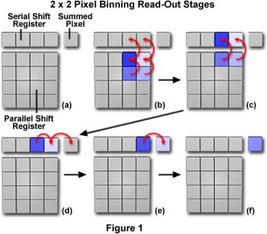
5 Binning
6 Bias

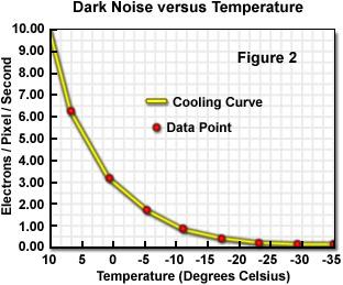
7 Dark Current
8 Flatfield


9 CCD Data Reduction Raw Bias + Dark Current Reduced Flatfield
10 Typical Array Detector Data Reduction science frame S, exposure time t S dark frame D, exposure time t D bias frame B, zero exposure time flat field frame F, exposure time t F corrected (calibrated) image given by S = S t s t D F t F t D ( D B) B ( D B) B F-(t f /t d) (D-B)-B often normalized such that mean of S = mean of S
 Charge Coupled Device")
11 CMOS and CCD Complementary Metal Oxide Semiconductor (CMOS) Charge Coupled Device (CCD)

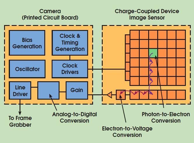
12 CMOS and CCD Cameras
13 CMOS vs. CCD CMOS advantages over CCD: standard semiconductor processing low power consumption ( 1% of CCD) random access to regions of interest blooming and streaking much reduced compared to CCDs additional electronics can be integrated on chip and in pixel (smart sensor) non-destructive readout CMOS disadvantages: small geometric fill factor (microlenses can help) typically larger read noise
14 Infrared Arrays Construction 1. Produce a grid of readout amplifiers 2. Produce a (matching mirror image) of detector pixels 3. Deposit Indium bumps on both sides 4. Squeeze the two planes together è hybrid arrays 5. The Indium will flow and provide electrical contact
15 Multiplexers Multiplexing: Pixel signals à Sequential output lines MUX Tasks: address a column of pixels by turning on their amplifiers pixels in other columns with power off will not contribute a signal Signal at photodiode à gate T 1 Readout uses row driver R 1 and column driver C 1 to close the switching transistors T 2, T 3, T 4. à Power to T 1 à signal to the output bus Reset: connect V R via T 5 and T 3.


16 Example: The Teledyne HAWAII-2RG See imaging/hawaii2rg.html for more info Can also be combined to a 2x2 mosaic
 Bias A/D Conv PreAmp")
17 Elements of a Detector Electronics System Example: PHARO (the Palomar High Angular Resolution Observer) Bias A/D Conv PreAmp Array
18 IR Array Read Out Modes Single Sampling Reset-Read-Read most simple approach does not remove ktc noise measures the absolute signal level (Multiple) Fowler Sampling Resets, reads and reads pixel-by-pixel Signal = Read(2) Read(1) best correlation, no reset noise but requires frame storage reduced dynamical range (saturation!) Sample-up-the-ramp Fitting similar to reset-read-read but each read is repeated m times Signal = mean(read2) mean(read1) Reduces readout noise by m over RRR m equidistant reads during integration linear fit à slope reduces readout noise by m particularly useful in space (cosmics!)
19 CCDs and IR Arrays are fundamentally different! CCDs: destructive reads charges are physically shifted to the output line shutter determines exposure time IR arrays: non-destructive reads readout requires sophisticated multiplexer circuit multiplexer readout addresses individual pixels directly read/reset determines exposure time
20 Basic Principle of a Bolometer A detector with thermal heat capacity C is connected via a thermal link of thermal conductance G to a heat sink of temperature T 0. The total power absorbed by the detector is: dt ( t) = GT1 + C dt P T 1 (doped silicon or germanium) measure the voltage across thermo. voltage depends on resistance resistance depends on temperature temperature depends on photon flux Bolometers are especially for the far-ir/sub-mm wavelength range!
21 QE and Composite Bolometers In some cases Si bolometers with high impurity concentrations can be very efficient absorbers. In many cases, however, the QE is too low. Solution: enhance absorption with black paint but this will increase the heat capacity. A high QE bolometer for far-ir and sub-mm would have too much heat capacity à composite bolometers. The heat capacity of the blackened sapphire plate is only 2% of that of Ge.
22 Etched Bolometers The bolometer design has been revolutionized by precision etching techniques in Si Thermal time response ~ C/G à small structures minimize the heat capacity C by reducing the volume of material.
23 Low Operating Temperatures 1. Four standard options to cool: 2. 4 He dewar (air pressure) à T=4.2K 3. 4 He dewar (pumped) à 1K<T <2K 4. 3 He (closed-cycle) refrigerator à T~0.3K 5. adiabatic demagnetization refrigerator à T ~ 0.1K Simplest solution is to use a twostage helium dewar (here: model from Infrared Laboratories, Inc.)


24 The array consists of 295 channels in 9 concentric hexagons. The array is under-sampled, thus special mapping techniques must be used. Bolometers an Overview The single pixel Ge:Ga bolometer invented in 1961 by Frank Low Herschel / PACS bolometer: a cut-out of the 64x32 pixel bolometer array assembly. LABOCA the multi-channel bolometer array for APEX operating in the 870 µm (345 GHz) atmospheric window. The signal photons are absorbed by a thin metal film cooled to about 280 mk.
25 Performance Comparison Bolometer ó Heterodyne Receiver Case 1: Bolometer operating at BLIP and heterodyne receiver operating in the thermal limit (hν«kt) è the bolometer will perform better This is always true, except for measurements at high spectral resolution, much higher than the IF bandwidth. Case 2: detector noise-limited bolometer and a heterodyne receiver operating at the quantum limit (hν»kt). è the heterodyne receiver will outperform the bolometer. In the case of narrow bandwidth and high spectral resolution the heterodyne system will always win.
26 MKIDS Physical Principle KID = Kinetic Inductance Detector MKID = Microwave KID
27 MKIDS Construction

28 MKIDS Operating Principle
VII. IR Arrays & Readout VIII.CCDs & Readout. This lecture course follows the textbook Detection of
 Detection of Light VII. IR Arrays & Readout VIII.CCDs & Readout This lecture course follows the textbook Detection of Light 4-3-2016 by George Rieke, Detection Cambridge of Light Bernhard Brandl University
Charged-Coupled Devices
 Charged-Coupled Devices Charged-Coupled Devices Useful texts: Handbook of CCD Astronomy Steve Howell- Chapters 2, 3, 4.4 Measuring the Universe George Rieke - 3.1-3.3, 3.6 CCDs CCDs were invented in 1969
Three Ways to Detect Light. We now establish terminology for photon detectors:
 Three Ways to Detect Light In photon detectors, the light interacts with the detector material to produce free charge carriers photon-by-photon. The resulting miniscule electrical currents are amplified
CCDS. Lesson I. Wednesday, August 29, 12
 CCDS Lesson I CCD OPERATION The predecessor of the CCD was a device called the BUCKET BRIGADE DEVICE developed at the Phillips Research Labs The BBD was an analog delay line, made up of capacitors such
Three Ways to Detect Light. Following: Lord Rosse image of M33 vs. Hubble image demonstrate how critical detector technology is.
 Three Ways to Detect Light In photon detectors, the light interacts with the detector material to produce free charge carriers photon-by-photon. The resulting miniscule electrical currents are amplified
Properties of a Detector
 Properties of a Detector Quantum Efficiency fraction of photons detected wavelength and spatially dependent Dynamic Range difference between lowest and highest measurable flux Linearity detection rate
Fundamentals of CMOS Image Sensors
 CHAPTER 2 Fundamentals of CMOS Image Sensors Mixed-Signal IC Design for Image Sensor 2-1 Outline Photoelectric Effect Photodetectors CMOS Image Sensor(CIS) Array Architecture CIS Peripherals Design Considerations
Detection Beyond 100µm Photon detectors no longer work ("shallow", i.e. low excitation energy, impurities only go out to equivalent of
 Detection Beyond 100µm Photon detectors no longer work ("shallow", i.e. low excitation energy, impurities only go out to equivalent of 100µm) A few tricks let them stretch a little further (like stressing)
Abstract. Preface. Acknowledgments
 Contents Abstract Preface Acknowledgments iv v vii 1 Introduction 1 1.1 A Very Brief History of Visible Detectors in Astronomy................ 1 1.2 The CCD: Astronomy s Champion Workhorse......................
Detectors for microscopy - CCDs, APDs and PMTs. Antonia Göhler. Nov 2014
 Detectors for microscopy - CCDs, APDs and PMTs Antonia Göhler Nov 2014 Detectors/Sensors in general are devices that detect events or changes in quantities (intensities) and provide a corresponding output,
Introduction to CCD camera
 Observational Astronomy 2011/2012 Introduction to CCD camera Charge Coupled Device (CCD) photo sensor coupled to shift register Jörg R. Hörandel Radboud University Nijmegen http://particle.astro.ru.nl/goto.html?astropract1-1112
Light gathering Power: Magnification with eyepiece:
 Telescopes Light gathering Power: The amount of light that can be gathered by a telescope in a given amount of time: t 1 /t 2 = (D 2 /D 1 ) 2 The larger the diameter the smaller the amount of time. If
CCD Analogy BUCKETS (PIXELS) HORIZONTAL CONVEYOR BELT (SERIAL REGISTER) VERTICAL CONVEYOR BELTS (CCD COLUMNS) RAIN (PHOTONS)
 HORIZONTAL CONVEYOR BELT (SERIAL REGISTER) VERTICAL CONVEYOR BELTS (CCD COLUMNS) RAIN (PHOTONS)") CCD Analogy RAIN (PHOTONS) VERTICAL CONVEYOR BELTS (CCD COLUMNS) BUCKETS (PIXELS) HORIZONTAL CONVEYOR BELT (SERIAL REGISTER) MEASURING CYLINDER (OUTPUT AMPLIFIER) Exposure finished, buckets now contain
CCD Analogy RAIN (PHOTONS) VERTICAL CONVEYOR BELTS (CCD COLUMNS) BUCKETS (PIXELS) HORIZONTAL CONVEYOR BELT (SERIAL REGISTER) MEASURING CYLINDER (OUTPUT AMPLIFIER) Exposure finished, buckets now contain
Dynamic Range. Can I look at bright and faint things at the same time?
 Detector Basics The purpose of any detector is to record the light collected by the telescope. All detectors transform the incident radiation into a some other form to create a permanent record, such as
Optical/IR Observational Astronomy Detectors II. David Buckley, SAAO
 David Buckley, SAAO 1 The Next Revolution: Charge Couple Device Detectors (CCDs) 2 Optical/IR Observational Astronomy CCDs Integrated semi-conductor detector From photon detection (pair production) to
First tests of prototype SCUBA-2 array
 First tests of prototype SCUBA-2 array Adam Woodcraft Astronomical Instrumentation Group School of Physics and Astronomy,Cardiff University http://woodcraft.lowtemp lowtemp.org/ Techniques and Instrumentation
High Resolution 640 x um Pitch InSb Detector
 High Resolution 640 x 512 15um Pitch InSb Detector Chen-Sheng Huang, Bei-Rong Chang, Chien-Te Ku, Yau-Tang Gau, Ping-Kuo Weng* Materials & Electro-Optics Division National Chung Shang Institute of Science
Charged Coupled Device (CCD) S.Vidhya
 S.Vidhya") Charged Coupled Device (CCD) S.Vidhya 02.04.2016 Sensor Physical phenomenon Sensor Measurement Output A sensor is a device that measures a physical quantity and converts it into a signal which can be read
Charged Coupled Device (CCD) S.Vidhya 02.04.2016 Sensor Physical phenomenon Sensor Measurement Output A sensor is a device that measures a physical quantity and converts it into a signal which can be read
Micro-sensors - what happens when you make "classical" devices "small": MEMS devices and integrated bolometric IR detectors
 Micro-sensors - what happens when you make "classical" devices "small": MEMS devices and integrated bolometric IR detectors Dean P. Neikirk 1 MURI bio-ir sensors kick-off 6/16/98 Where are the targets
Detectors that cover a dynamic range of more than 1 million in several dimensions
 Detectors that cover a dynamic range of more than 1 million in several dimensions Detectors for Astronomy Workshop Garching, Germany 10 October 2009 James W. Beletic Teledyne Providing the best images
IV DETECTORS. Daguerrotype of the Moon, John W. Draper. March 26, 1840 New York
 IV DETECTORS Lit.: C.R.Kitchin: Astrophysical Techniques, 2009 C.D.Mckay: CCD s in Astronomy, Ann.Rev. A.&A. 24, 1986 G.H.Rieke: Infrared Detector Arrays for Astronomy, Ann.Rev. A&A 45, 2007 up to 1837:
Jan Bogaerts imec
 imec 2007 1 Radiometric Performance Enhancement of APS 3 rd Microelectronic Presentation Days, Estec, March 7-8, 2007 Outline Introduction Backside illuminated APS detector Approach CMOS APS (readout)
Digital camera. Sensor. Memory card. Circuit board
 Digital camera Circuit board Memory card Sensor Detector element (pixel). Typical size: 2-5 m square Typical number: 5-20M Pixel = Photogate Photon + Thin film electrode (semi-transparent) Depletion volume
Last class. This class. CCDs Fancy CCDs. Camera specs scmos
 CCDs and scmos Last class CCDs Fancy CCDs This class Camera specs scmos Fancy CCD cameras: -Back thinned -> higher QE -Unexposed chip -> frame transfer -Electron multiplying -> higher SNR -Fancy ADC ->
Charge-Coupled Device (CCD) Detectors pixel silicon chip electronics cryogenics
 Detectors pixel silicon chip electronics cryogenics") Charge-Coupled Device (CCD) Detectors As revolutionary in astronomy as the invention of the telescope and photography semiconductor detectors a collection of miniature photodiodes, each called a picture
Charge-Coupled Device (CCD) Detectors As revolutionary in astronomy as the invention of the telescope and photography semiconductor detectors a collection of miniature photodiodes, each called a picture
STA1600LN x Element Image Area CCD Image Sensor
 ST600LN 10560 x 10560 Element Image Area CCD Image Sensor FEATURES 10560 x 10560 Photosite Full Frame CCD Array 9 m x 9 m Pixel 95.04mm x 95.04mm Image Area 100% Fill Factor Readout Noise 2e- at 50kHz
Introduction. Chapter 1
 1 Chapter 1 Introduction During the last decade, imaging with semiconductor devices has been continuously replacing conventional photography in many areas. Among all the image sensors, the charge-coupled-device
Two-phase full-frame CCD with double ITO gate structure for increased sensitivity
 Two-phase full-frame CCD with double ITO gate structure for increased sensitivity William Des Jardin, Steve Kosman, Neal Kurfiss, James Johnson, David Losee, Gloria Putnam *, Anthony Tanbakuchi (Eastman
ABSTRACT. Section I Overview of the µdss
 An Autonomous Low Power High Resolution micro-digital Sun Sensor Ning Xie 1, Albert J.P. Theuwissen 1, 2 1. Delft University of Technology, Delft, the Netherlands; 2. Harvest Imaging, Bree, Belgium; ABSTRACT
TDI Imaging: An Efficient AOI and AXI Tool
 TDI Imaging: An Efficient AOI and AXI Tool Yakov Bulayev Hamamatsu Corporation Bridgewater, New Jersey Abstract As a result of heightened requirements for quality, integrity and reliability of electronic
CCD1600A Full Frame CCD Image Sensor x Element Image Area
 - 1 - General Description CCD1600A Full Frame CCD Image Sensor 10560 x 10560 Element Image Area General Description The CCD1600 is a 10560 x 10560 image element solid state Charge Coupled Device (CCD)
Astro-photography. Daguerreotype: on a copper plate
 AST 1022L Astro-photography 1840-1980s: Photographic plates were astronomers' main imaging tool At right: first ever picture of the full moon, by John William Draper (1840) Daguerreotype: exposure using
CCD and CMOS Imaging Devices for Large (Ground Based) Telescopes. Veljko Radeka BNL SNIC April 3, 2006
 Telescopes. Veljko Radeka BNL SNIC April 3, 2006") CCD and CMOS Imaging Devices for Large (Ground Based) Telescopes Veljko Radeka BNL SNIC April 3, 2006 1 Large Telescopes Survey telescope Deep probe Primary Mirror dia.=d m, Area= A Large (~8m) Very large
CCD and CMOS Imaging Devices for Large (Ground Based) Telescopes Veljko Radeka BNL SNIC April 3, 2006 1 Large Telescopes Survey telescope Deep probe Primary Mirror dia.=d m, Area= A Large (~8m) Very large
IT FR R TDI CCD Image Sensor
 4k x 4k CCD sensor 4150 User manual v1.0 dtd. August 31, 2015 IT FR 08192 00 R TDI CCD Image Sensor Description: With the IT FR 08192 00 R sensor ANDANTA GmbH builds on and expands its line of proprietary
DV420 SPECTROSCOPY. issue 2 rev 1 page 1 of 5m. associated with LN2
 SPECTROSCOPY Andor s DV420 CCD cameras offer the best price/performance for a wide range of spectroscopy applications. The 1024 x 256 array with 26µm 2 pixels offers the best dynamic range versus resolution.
Semiconductor Detector Systems
 Semiconductor Detector Systems Helmuth Spieler Physics Division, Lawrence Berkeley National Laboratory OXFORD UNIVERSITY PRESS ix CONTENTS 1 Detector systems overview 1 1.1 Sensor 2 1.2 Preamplifier 3
READOUT TECHNIQUES FOR DRIFT AND LOW FREQUENCY NOISE REJECTION IN INFRARED ARRAYS
 READOUT TECHNIQUES FOR DRIFT AND LOW FREQUENCY NOISE REJECTION IN INFRARED ARRAYS Finger 1, G, Dorn 1, R.J 1, Hoffman, A.W. 2, Mehrgan, H. 1, Meyer, M. 1, Moorwood A.F.M. 1 and Stegmeier, J. 1 1) European
An Introduction to CCDs. The basic principles of CCD Imaging is explained.
 An Introduction to CCDs. The basic principles of CCD Imaging is explained. Morning Brain Teaser What is a CCD? Charge Coupled Devices (CCDs), invented in the 1970s as memory devices. They improved the
Charge Coupled Devices. C. A. Griffith, Class Notes, PTYS 521, 2016 Not for distribution.
 Charge Coupled Devices C. A. Griffith, Class Notes, PTYS 521, 2016 Not for distribution. 1 1. Introduction While telescopes are able to gather more light from a distance source than does the naked eye,
DIGITAL IMAGING. Handbook of. Wiley VOL 1: IMAGE CAPTURE AND STORAGE. Editor-in- Chief
 Handbook of DIGITAL IMAGING VOL 1: IMAGE CAPTURE AND STORAGE Editor-in- Chief Adjunct Professor of Physics at the Portland State University, Oregon, USA Previously with Eastman Kodak; University of Rochester,
ACTIVE PIXEL SENSORS VS. CHARGE-COUPLED DEVICES
 ACTIVE PIXEL SENSORS VS. CHARGE-COUPLED DEVICES Dr. Eric R. Fossum Imaging Systems Section Jet Propulsion Laboratory, California Institute of Technology (818) 354-3128 1993 IEEE Workshop on CCDs and Advanced
Minimizes reflection losses from UV-IR; Optional AR coatings & wedge windows are available.
 Now Powered by LightField PyLoN:2K 2048 x 512 The PyLoN :2K is a controllerless, cryogenically-cooled CCD camera designed for quantitative scientific spectroscopy applications demanding the highest possible
Laboratory, University of Arizona, Tucson, AZ 85721; c ImagerLabs, 1995 S. Myrtle Ave., Monrovia CA INTRODUCTION ABSTRACT
 A CMOS Visible Image Sensor with Non-Destructive Readout Capability Gary R. Sims* a, Gene Atlas c, Eric Christensen b, Roger W. Cover a, Stephen Larson b, Hans J. Meyer a, William V. Schempp a a Spectral

CCD Characteristics Lab
 CCD Characteristics Lab Observational Astronomy 6/6/07 1 Introduction In this laboratory exercise, you will be using the Hirsch Observatory s CCD camera, a Santa Barbara Instruments Group (SBIG) ST-8E.
EE 392B: Course Introduction
 EE 392B Course Introduction About EE392B Goals Topics Schedule Prerequisites Course Overview Digital Imaging System Image Sensor Architectures Nonidealities and Performance Measures Color Imaging Recent
Part I. CCD Image Sensors
 Part I CCD Image Sensors 2 Overview of CCD CCD is the abbreviation for charge-coupled device. CCD image sensors are silicon-based integrated circuits (ICs), consisting of a dense matrix of photodiodes
Overview. Charge-coupled Devices. MOS capacitor. Charge-coupled devices. Charge-coupled devices:
 Overview Charge-coupled Devices Charge-coupled devices: MOS capacitors Charge transfer Architectures Color Limitations 1 2 Charge-coupled devices MOS capacitor The most popular image recording technology
Simulation of High Resistivity (CMOS) Pixels
 Pixels") Simulation of High Resistivity (CMOS) Pixels Stefan Lauxtermann, Kadri Vural Sensor Creations Inc. AIDA-2020 CMOS Simulation Workshop May 13 th 2016 OUTLINE 1. Definition of High Resistivity Pixel Also
Simulation of High Resistivity (CMOS) Pixels Stefan Lauxtermann, Kadri Vural Sensor Creations Inc. AIDA-2020 CMOS Simulation Workshop May 13 th 2016 OUTLINE 1. Definition of High Resistivity Pixel Also
An Introduction to Scientific Imaging C h a r g e - C o u p l e d D e v i c e s
 p a g e 2 S C I E N T I F I C I M A G I N G T E C H N O L O G I E S, I N C. Introduction to the CCD F u n d a m e n t a l s The CCD Imaging A r r a y An Introduction to Scientific Imaging C h a r g e -
Cameras CS / ECE 181B
 Cameras CS / ECE 181B Image Formation Geometry of image formation (Camera models and calibration) Where? Radiometry of image formation How bright? What color? Examples of cameras What is a Camera? A camera
Photons and solid state detection
 Photons and solid state detection Photons represent discrete packets ( quanta ) of optical energy Energy is hc/! (h: Planck s constant, c: speed of light,! : wavelength) For solid state detection, photons
TEST RESULTS WITH 2KX2K MCT ARRAYS
 TEST RESULTS WITH 2KX2K MCT ARRAYS Finger, G, Dorn, R.J., Mehrgan, H., Meyer, M., Moorwood A.F.M. and Stegmeier, J. European Southern Observatory Abstract: Key words: The performance of both an LPE 2Kx2K
Fully depleted, thick, monolithic CMOS pixels with high quantum efficiency
 Fully depleted, thick, monolithic CMOS pixels with high quantum efficiency Andrew Clarke a*, Konstantin Stefanov a, Nicholas Johnston a and Andrew Holland a a Centre for Electronic Imaging, The Open University,
The Charge-Coupled Device. Many overheads courtesy of Simon Tulloch
 The Charge-Coupled Device Astronomy 1263 Many overheads courtesy of Simon Tulloch smt@ing.iac.es Jan 24, 2013 What does a CCD Look Like? The fine surface electrode structure of a thick CCD is clearly visible
Where detectors are used in science & technology
 Lecture 9 Outline Role of detectors Photomultiplier tubes (photoemission) Modulation transfer function Photoconductive detector physics Detector architecture Where detectors are used in science & technology
Ultra-high resolution 14,400 pixel trilinear color image sensor
 Ultra-high resolution 14,400 pixel trilinear color image sensor Thomas Carducci, Antonio Ciccarelli, Brent Kecskemety Microelectronics Technology Division Eastman Kodak Company, Rochester, New York 14650-2008
CMOS Today & Tomorrow
 CMOS Today & Tomorrow Uwe Pulsfort TDALSA Product & Application Support Overview Image Sensor Technology Today Typical Architectures Pixel, ADCs & Data Path Image Quality Image Sensor Technology Tomorrow
The new CMOS Tracking Camera used at the Zimmerwald Observatory
 13-0421 The new CMOS Tracking Camera used at the Zimmerwald Observatory M. Ploner, P. Lauber, M. Prohaska, P. Schlatter, J. Utzinger, T. Schildknecht, A. Jaeggi Astronomical Institute, University of Bern,
Image Formation and Capture. Acknowledgment: some figures by B. Curless, E. Hecht, W.J. Smith, B.K.P. Horn, and A. Theuwissen
 Image Formation and Capture Acknowledgment: some figures by B. Curless, E. Hecht, W.J. Smith, B.K.P. Horn, and A. Theuwissen Image Formation and Capture Real world Optics Sensor Devices Sources of Error
a simple optical imager
 Imagers and Imaging a simple optical imager Here s one on our 61-Inch Telescope Here s one on our 61-Inch Telescope filter wheel in here dewar preamplifier However, to get a large field we cannot afford
J. Janesick, S.A. Collins, and E.R. Fossum Imaging Systems Section Jet Propulsion Laboratory Pasadena, CA 91109
 Scientific CCD Technology at JPL J. Janesick, S.A. Collins, and E.R. Fossum maging Systems Section Jet Propulsion Laboratory Pasadena, CA 91109 ntroduction Charge-coupled devices (CCOs) were recognized
Tunable wideband infrared detector array for global space awareness
 Tunable wideband infrared detector array for global space awareness Jonathan R. Andrews 1, Sergio R. Restaino 1, Scott W. Teare 2, Sanjay Krishna 3, Mike Lenz 3, J.S. Brown 3, S.J. Lee 3, Christopher C.
Welcome to: LMBR Imaging Workshop. Imaging Fundamentals Mike Meade, Photometrics
 Welcome to: LMBR Imaging Workshop Imaging Fundamentals Mike Meade, Photometrics Introduction CCD Fundamentals Typical Cooled CCD Camera Configuration Shutter Optic Sealed Window DC Voltage Serial Clock
More Imaging Luc De Mey - CEO - CMOSIS SA
 More Imaging Luc De Mey - CEO - CMOSIS SA Annual Review / June 28, 2011 More Imaging CMOSIS: Vision & Mission CMOSIS s Business Concept On-Going R&D: More Imaging CMOSIS s Vision Image capture is a key
THE CCD RIDDLE REVISTED: SIGNAL VERSUS TIME LINEAR SIGNAL VERSUS VARIANCE NON-LINEAR
 THE CCD RIDDLE REVISTED: SIGNAL VERSUS TIME LINEAR SIGNAL VERSUS VARIANCE NON-LINEAR Mark Downing 1, Peter Sinclaire 1. 1 ESO, Karl Schwartzschild Strasse-2, 85748 Munich, Germany. ABSTRACT The photon
The 0.84 m Telescope OAN/SPM - BC, Mexico
 The 0.84 m Telescope OAN/SPM - BC, Mexico Readout error CCD zero-level (bias) ramping CCD bias frame banding Shutter failure Significant dark current Image malting Focus frame taken during twilight IR
Chapter 3: Sensing the light: Detectors for the Optical and Infrared
 Chapter 3: Sensing the light: Detectors for the Optical and Infrared 3.1 Basic Properties of Photo-detectors Modern photon detectors operate by placing a bias voltage across a semiconductor crystal, illuminating
Receiver Performance and Comparison of Incoherent (bolometer) and Coherent (receiver) detection
 and Coherent (receiver) detection") At ev gap /h the photons have sufficient energy to break the Cooper pairs and the SIS performance degrades. Receiver Performance and Comparison of Incoherent (bolometer) and Coherent (receiver) detection
At ev gap /h the photons have sufficient energy to break the Cooper pairs and the SIS performance degrades. Receiver Performance and Comparison of Incoherent (bolometer) and Coherent (receiver) detection
3/27/17. Detector Basics. Quantum Efficiency (QE) and Spectral Response. Quantum Efficiency (QE) and Spectral Response
 and Spectral Response. Quantum Efficiency (QE) and Spectral Response") 3/27/17 Detector Basics The purpose of any detector is to record the light collected by the telescope. All detectors transform the incident radiation into a some other form to create a permanent record,
3/27/17 Detector Basics The purpose of any detector is to record the light collected by the telescope. All detectors transform the incident radiation into a some other form to create a permanent record,
Design of an Integrated Image Sensor System
 Institute of Integrated Sensor Systems Dept. of Electrical Engineering and Information Technology Design of an Integrated Image Sensor System Kuan Shang Fall Semester, 2007 Prof. Dr.-Ing. Andreas König
Lecture 29: Image Sensors. Computer Graphics and Imaging UC Berkeley CS184/284A
 Lecture 29: Image Sensors Computer Graphics and Imaging UC Berkeley Photon Capture The Photoelectric Effect Incident photons Ejected electrons Albert Einstein (wikipedia) Einstein s Nobel Prize in 1921
Advances in Far-Infrared Detector Technology. Jonas Zmuidzinas Caltech/JPL
 Advances in Far-Infrared Detector Technology Jonas Zmuidzinas Caltech/JPL December 1, 2016 OST vs Herschel: ~x gain from aperture Remaining gain from lower background with 4K telescope 2 OST vs Herschel:
Introduction to Computer Vision
 Introduction to Computer Vision CS / ECE 181B Thursday, April 1, 2004 Course Details HW #0 and HW #1 are available. Course web site http://www.ece.ucsb.edu/~manj/cs181b Syllabus, schedule, lecture notes,
Lecture 7. July 24, Detecting light (converting light to electrical signal)
") Lecture 7 July 24, 2017 Detecting light (converting light to electrical signal) Photoconductor Photodiode Managing electrical signal Metal-oxide-semiconductor (MOS) capacitor Charge coupled device (CCD)
Lecture 7 July 24, 2017 Detecting light (converting light to electrical signal) Photoconductor Photodiode Managing electrical signal Metal-oxide-semiconductor (MOS) capacitor Charge coupled device (CCD)
A Summary of Charge-Coupled Devices for Astronomy
 PUBLICATIONS OF THE ASTRONOMICAL SOCIETY OF THE PACIFIC, 127:1097 1104, 2015 November 2015. The Astronomical Society of the Pacific. All rights reserved. Printed in U.S.A. A Summary of Charge-Coupled Devices
EE 5611 Introduction to Microelectronic Technologies Fall Thursday, September 04, 2014 Lecture 02
 EE 5611 Introduction to Microelectronic Technologies Fall 2014 Thursday, September 04, 2014 Lecture 02 1 Lecture Outline Review on semiconductor materials Review on microelectronic devices Example of microelectronic
EVALUATION OF RADIATION HARDNESS DESIGN TECHNIQUES TO IMPROVE RADIATION TOLERANCE FOR CMOS IMAGE SENSORS DEDICATED TO SPACE APPLICATIONS
 EVALUATION OF RADIATION HARDNESS DESIGN TECHNIQUES TO IMPROVE RADIATION TOLERANCE FOR CMOS IMAGE SENSORS DEDICATED TO SPACE APPLICATIONS P. MARTIN-GONTHIER, F. CORBIERE, N. HUGER, M. ESTRIBEAU, C. ENGEL,
Digital Imaging Rochester Institute of Technology
 Digital Imaging 1999 Rochester Institute of Technology So Far... camera AgX film processing image AgX photographic film captures image formed by the optical elements (lens). Unfortunately, the processing
High-end CMOS Active Pixel Sensor for Hyperspectral Imaging
 R11 High-end CMOS Active Pixel Sensor for Hyperspectral Imaging J. Bogaerts (1), B. Dierickx (1), P. De Moor (2), D. Sabuncuoglu Tezcan (2), K. De Munck (2), C. Van Hoof (2) (1) Cypress FillFactory, Schaliënhoevedreef
3/5/17. Detector Basics. Quantum Efficiency (QE) and Spectral Response. Quantum Efficiency (QE) and Spectral Response
 and Spectral Response. Quantum Efficiency (QE) and Spectral Response") 3/5/17 Detector Basics The purpose of any detector is to record the light collected by the telescope. All detectors transform the incident radiation into a some other form to create a permanent record,
3/5/17 Detector Basics The purpose of any detector is to record the light collected by the telescope. All detectors transform the incident radiation into a some other form to create a permanent record,
What an Observational Astronomer needs to know!
 What an Observational Astronomer needs to know! IRAF:Photometry D. Hatzidimitriou Masters course on Methods of Observations and Analysis in Astronomy Basic concepts Counts how are they related to the actual
Submillimeter (continued)
") Submillimeter (continued) Dual Polarization, Sideband Separating Receiver Dual Mixer Unit The 12-m Receiver Here is where the receiver lives, at the telescope focus Receiver Performance T N (noise temperature)
Submillimeter (continued) Dual Polarization, Sideband Separating Receiver Dual Mixer Unit The 12-m Receiver Here is where the receiver lives, at the telescope focus Receiver Performance T N (noise temperature)
Lecture 8 Optical Sensing. ECE 5900/6900 Fundamentals of Sensor Design
 ECE 5900/6900: Fundamentals of Sensor Design Lecture 8 Optical Sensing 1 Optical Sensing Q: What are we measuring? A: Electromagnetic radiation labeled as Ultraviolet (UV), visible, or near,mid-, far-infrared
Components of Optical Instruments
 Components of Optical Instruments General Design of Optical Instruments Sources of Radiation Wavelength Selectors (Filters, Monochromators, Interferometers) Sample Containers Radiation Transducers (Detectors)
Image acquisition. In both cases, the digital sensing element is one of the following: Line array Area array. Single sensor
 Image acquisition Digital images are acquired by direct digital acquisition (digital still/video cameras), or scanning material acquired as analog signals (slides, photographs, etc.). In both cases, the
Silicon sensors for radiant signals. D.Sc. Mikko A. Juntunen
 Silicon sensors for radiant signals D.Sc. Mikko A. Juntunen 2017 01 16 Today s outline Introduction Basic physical principles PN junction revisited Applications Light Ionizing radiation X-Ray sensors in
INTRODUCTION TO CCD IMAGING
 ASTR 1030 Astronomy Lab 85 Intro to CCD Imaging INTRODUCTION TO CCD IMAGING SYNOPSIS: In this lab we will learn about some of the advantages of CCD cameras for use in astronomy and how to process an image.
BACKSIDE ILLUMINATED CMOS-TDI LINE SCANNER FOR SPACE APPLICATIONS
 BACKSIDE ILLUMINATED CMOS-TDI LINE SCANNER FOR SPACE APPLICATIONS O. Cohen, N. Ben-Ari, I. Nevo, N. Shiloah, G. Zohar, E. Kahanov, M. Brumer, G. Gershon, O. Ofer SemiConductor Devices (SCD) P.O.B. 2250,
High-speed Ge photodetector monolithically integrated with large cross silicon-on-insulator waveguide
 [ APPLIED PHYSICS LETTERS ] High-speed Ge photodetector monolithically integrated with large cross silicon-on-insulator waveguide Dazeng Feng, Shirong Liao, Roshanak Shafiiha. etc Contents 1. Introduction
Image Formation and Capture
 Figure credits: B. Curless, E. Hecht, W.J. Smith, B.K.P. Horn, A. Theuwissen, and J. Malik Image Formation and Capture COS 429: Computer Vision Image Formation and Capture Real world Optics Sensor Devices
Basic CCD imaging CCD/CMOS Cameras
 Pedro Ré (2018) http:/re.apaaweb.com Basic CCD imaging CCD/CMOS Cameras There are basically five different kinds of digital cameras: 1. Dedicated, Cooled Astronomical CCD Cameras (CCD) 2. Digital SLR Cameras
Lecture: Integration of silicon photonics with electronics. Prepared by Jean-Marc FEDELI CEA-LETI
 Lecture: Integration of silicon photonics with electronics Prepared by Jean-Marc FEDELI CEA-LETI Context The goal is to give optical functionalities to electronics integrated circuit (EIC) The objectives
Acknowledgements CEA-Saclay / SAp Boulade Olivier, Doumayrou Eric, Horeau Benoit, Lepennec Yannick, Martignac Jerome, Okumura Koryo, Révéret Vincent,
 Recent Achievements in the Development of HERSCHEL/PACS Bolometer Arrays Nicolas BILLOT nbillot@cea.fr CEA - Saclay/DAPNIA/SAp UMR - Astrophysique Interaction Multi-echelle Acknowledgements CEA-Saclay
WHITE PAPER. Guide to CCD-Based Imaging Colorimeters
 Guide to CCD-Based Imaging Colorimeters How to choose the best imaging colorimeter CCD-based instruments offer many advantages for measuring light and color. When configured effectively, CCD imaging systems
Submillimeter Instrumentation. Photo-detectors are no longer effective Submm astronomers use bolometers and heterodyne receivers.
 Submillimeter Instrumentation Photo-detectors are no longer effective Submm astronomers use bolometers and heterodyne receivers. Bolometers A bolometer consists of an absorber (efficiency ) attached to
Control of Noise and Background in Scientific CMOS Technology
 Control of Noise and Background in Scientific CMOS Technology Introduction Scientific CMOS (Complementary metal oxide semiconductor) camera technology has enabled advancement in many areas of microscopy
Design of Sub-Wavelength Color Filters Design and Simulation with the RSoft Tools Synopsys, Inc. 1
 Design of Sub-Wavelength Color Filters Design and Simulation with the RSoft Tools 2018 Synopsys, Inc. 1 Outline Introduction Plasmonic color filters Dielectric color filters Related Topics Conclusion 2018
Detailed Characterisation of a New Large Area CCD Manufactured on High Resistivity Silicon
 Detailed Characterisation of a New Large Area CCD Manufactured on High Resistivity Silicon Mark S. Robbins *, Pritesh Mistry, Paul R. Jorden e2v technologies Ltd, 106 Waterhouse Lane, Chelmsford, Essex
Observing*Checklist:*A3ernoon*
 Ay#122a:# Intro#to#Observing/Image#Processing# (Many&slides&today& c/o&m.&bolte)& Observing*Checklist:*A3ernoon* Set*up*instrument*(verify*and*set*filters,*gra@ngs,*etc.)* Set*up*detector*(format,*gain,*binning)*