Time Delay Integration (TDI), The Answer to Demands for Increasing Frame Rate/Sensitivity? Craige Palmer Assistant Sales Manager
|
|
|
- Ella Ashlyn Murphy
- 6 years ago
- Views:
Transcription

1 Time Delay Integration (TDI), The Answer to Demands for Increasing Frame Rate/Sensitivity? Craige Palmer Assistant Sales Manager

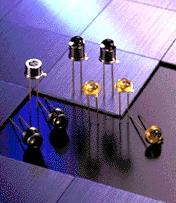
2 Laser Scanning Microscope High Speed Gated PMT Module High Speed Gating : 30nS~DC High Repetition : ~ 100kHz Input voltage 15Vdc Protection Circuits Gain adjustable H7680 PMT HVPS GATE Timing Protect Power Supply Circuits Signal Vcont Gate Pulse LED Parameter C1392 New Gated PMT module Gate Width 1uS to 10uS 30nS to DC Repetition 10kHz 100kHz max Switching Ratio 1e4 1e7 Gate Noise 3.5 to 35mV 20mV +15V GND


3 Applications MTP Reader Excitation Lasers PHOTOSENSOR MODULE Printing Process Control (include Banknote Printing) Excitation Laser MTP PHOTOSENSOR MODULE Pearl Cell Analyzer Sample PHOTOSENSO R MODULE PHOTOSENSOR MODULE Color Selection of Pearl
 Wide Dynamic")
4 What are NMOS/CMOS Image Sensors? Self Scanning Photodiode Array Large Sensitive Area Direct UV Sensitivity (stable) Wide Dynamic Range High Saturation Charge Good Linearity Low Power Consumption

5 What benefits does this give? Simpler circuit Low voltage operation Smaller package dimensions

6 Back Thinned CCD Modules High Speed Camera Module Features 1k x 1k back thinned CCD Chip > 90 % QE 10 MHz pixel readout rate LVDS interface
7 Movement of object Synchronize CCD vertical transfer Exposure/Acc umulation within the number of stages
8 Line Sensor Operation [Sample] [Output signal from a line sensor] Output image Line sensor Optical image
9 TDI Operation [Sample] [TDI sensor (4 stages)] Output image Signal intensity TDI sensor Optical image
10 TDI vs Line Sensor Comparison [Sample] [Line sensor] [TDI sensor (4 stages)] TDI stages = Higher Output

11 Advantage of TDI operation Higher sensitivity than line sensor High sensitivity is realized by multiplication of exposure and charge accumulation due to a number of vertical stages. Higher speed than area sensor High-speed readout is realized by synchronization of moving object and multi-tap. Bi-directional transfer
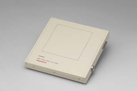
12 OEM camera w/o chassis Front illuminated or back thinned SSD rectangular CCD chips with 1TE (0 Deg C) USB2.0 TDI or Vertical binning (Factory setting) Frame readout for focusing DC 12V DCAM-API support and sample software for spectroscopic imaging

x38(V)x140(D)")
13 Appearance Standard configurations *Sensor head 96(H)x84(V)x65(D) *Control PCB 54(H)x38(V)x140(D) Chassis for demo use
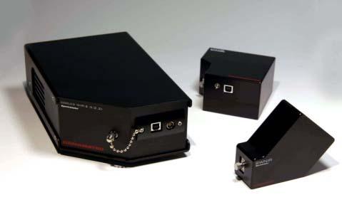
14 C10000 Series TDI Camera SSD Back Thinned TDI CCD Higher speed (50 khz) 12 bit / 8 bit ADC Board Level - Already Available
15 C10000 Series TDI Camera C / -401 (1K x 128/2TAP, 2k x 128/4TAP) DSP (Tap difference and shading correction) DC+12V (DC-DC Converter) C / -701 (4K x 128/8TAP, 4K x 128/16TAP) DSP (Tap difference and shading correction) DC+12V (DC-DC Converter)


16 C10000 Series TDI Camera RAW IMAGE Shading correction by DSP C / -401 C / -701

17 Back thinned sensor/high QE -Maximum QE : Higher than 90 % -Higher than 50 % at 200 nm -Higher than 20% at 1000 nm Features
18 Features Frame readout mode Easy for focusing and alignment Bi-directional readout in TDI mode Object can move in either direction Anti-blooming with lateral overflow drain Overflow charge from saturation pixels can be drained. Upto 100x of saturation level.
19 C10650 Series High Resolution/High Sensitivity 3072 (1536 x 2 chips) x (1536 x 3 chips) x 128 Direct X-Ray Imaging (FOP+CsI) Realtime Dark Current/Shading Correction CameraLink Interface
20 C10650 Series
21 C10650 Series Dark current (back ground) correction To get higher Dynamic range To correct dark current range in each module Sensitivity (Brightness) correction X-ray source shading correction Sensitivity correction on sensor Sensitivity correction on scintillator


22 Applications Dimensions control e.g. Cans, Boxes Dental Aerial Reconnaissance


23 Medical Slide Scanner X Z TDI Sensor Simple stage control for 2D measurement. Inexpensive TDI sensor for a large area scanning with high resolution imaging. Y High speed imaging with high resolution by TDI.

24 Semiconductor - Wafer Defects/Voids TDI camera Motion stage/rotation Light source


25 Flow Cytometry PMT system TDI system Excitation Fluorescence Excitation Fluorescence TDI camera intensity time Mean intensity only can be measured Both intensity and image can be determined


26 MTP Reader - Increase speed - Minimise sample damage Conventional TDI system Fluorescence TDI camera Excitation Excitation Fluorescence PMT or camera


27 On line Inspection Conventional - strobe flash light and electrical shutter of CCD sensor. CMOS sensor is used for these purpose. (S/N is bad!!) LED light source (limited intensity) TDI technology = Speed, sensitivity and continuous acquisition. High-speed motion of object Flash illumination TDI camera
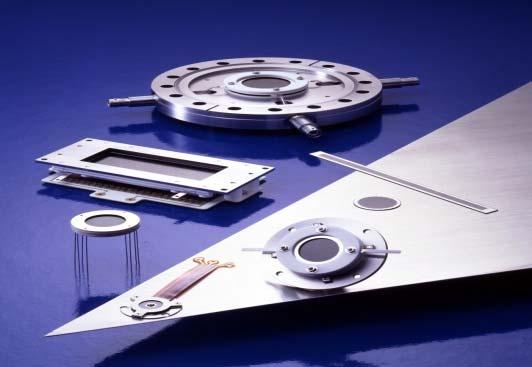
28 Possible to detect: Scratches, Seams, Cracks Steel Inspection

29 Letter Sorting Barcode reading Character Recognition Stamp detection Print quality verification

30 Glass Inspection Possible to inspect blemish or scratch on a large size glass with high speed by bi-directional readout. TDI camera Motion stage

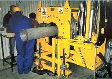
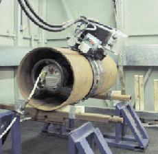
31 X-Ray Non-Destructive Testing Microfocus X-ray source + X-ray TDI Camera Magnify the defect for detailed analysis Good dynamic range for speed variation Components Inspection


32 X-Ray Non-Destructive Testing Components Inspection Only digital zoom!

33 X-Ray Non-Destructive Testing Stainless Steel Ball Components Inspection

34 X-Ray Non-Destructive Testing Can Inspection

35 X-Ray Non-Destructive Testing Drug Inspection

36 X-Ray Non-Destructive Testing Weld Inspection


37 Hamamatsu Solid State Products Photodiodes and PSDs CCD, CMOS and IR Image Sensors Mini Spectrometers Avalanche Photodiodes ( APDs ) Laser Diodes Flat Panel X-Ray Imagers Photo IC s LEDs Infrared Detectors


38 Hamamatsu Tube Products Photomultiplier Tubes ( PMTs ) PMT Modules Image Intensifiers Microfocus X-Ray Sources X-ray Scintillators and FOPs X-Ray Image Intensifiers D2, Xenon, Hg & Flash Lamps MCPs and Ion Detectors UV and Visible Light Sources


39 Hamamatsu Systems Products Scientific Digital Cameras AquaCosmos for BiotechnologyBoard Cameras for Industry Nanozoomer Slide Scanner FDSS Drug Screening System NIRO Oxygenation Monitor Semiconductor Failure Analysis X-ray Sensors & Cameras Streak Cameras and Ultra High Speed Imaging

40 VISIT OUR WEBSITE or Stand No. BO1 or Contact Our Office: Hamamatsu Photonics U.K. Ltd Tel:
Detectors for microscopy - CCDs, APDs and PMTs. Antonia Göhler. Nov 2014
 Detectors for microscopy - CCDs, APDs and PMTs Antonia Göhler Nov 2014 Detectors/Sensors in general are devices that detect events or changes in quantities (intensities) and provide a corresponding output,
IT FR R TDI CCD Image Sensor
 4k x 4k CCD sensor 4150 User manual v1.0 dtd. August 31, 2015 IT FR 08192 00 R TDI CCD Image Sensor Description: With the IT FR 08192 00 R sensor ANDANTA GmbH builds on and expands its line of proprietary
TDI Imaging: An Efficient AOI and AXI Tool
 TDI Imaging: An Efficient AOI and AXI Tool Yakov Bulayev Hamamatsu Corporation Bridgewater, New Jersey Abstract As a result of heightened requirements for quality, integrity and reliability of electronic
CMOS Today & Tomorrow
 CMOS Today & Tomorrow Uwe Pulsfort TDALSA Product & Application Support Overview Image Sensor Technology Today Typical Architectures Pixel, ADCs & Data Path Image Quality Image Sensor Technology Tomorrow
Applications for cameras with CMOS-, CCD- and InGaAssensors. Jürgen Bretschneider AVT, 2014
 Applications for cameras with CMOS-, CCD- and InGaAssensors Jürgen Bretschneider AVT, 2014 Allied Vision Technologies Profile Foundation: 1989,Headquarters: Stadtroda (Thüringen), Employees: aprox. 265
Last class. This class. CCDs Fancy CCDs. Camera specs scmos
 CCDs and scmos Last class CCDs Fancy CCDs This class Camera specs scmos Fancy CCD cameras: -Back thinned -> higher QE -Unexposed chip -> frame transfer -Electron multiplying -> higher SNR -Fancy ADC ->
SOLAR CELL INSPECTION WITH RAPTOR PHOTONICS OWL (SWIR) AND FALCON (EMCCD)
 AND FALCON (EMCCD)") Technical Note Solar Cell Inspection SOLAR CELL INSPECTION WITH RAPTOR PHOTONICS OWL (SWIR) AND FALCON (EMCCD) August 2012, Northern Ireland Solar cell inspection relies on imaging the photoluminescence
Technical Note Solar Cell Inspection SOLAR CELL INSPECTION WITH RAPTOR PHOTONICS OWL (SWIR) AND FALCON (EMCCD) August 2012, Northern Ireland Solar cell inspection relies on imaging the photoluminescence
Light Microscopy for Biomedical Research
 Light Microscopy for Biomedical Research Tuesday 4:30 PM Quantification & Digital Images Michael Hooker Microscopy Facility Michael Chua microscopy@unc.edu 843-3268 6007 Thurston Bowles http://microscopy.unc.edu/lmbr
pco.edge 4.2 LT 0.8 electrons 2048 x 2048 pixel 40 fps up to :1 up to 82 % pco. low noise high resolution high speed high dynamic range
 edge 4.2 LT scientific CMOS camera high resolution 2048 x 2048 pixel low noise 0.8 electrons USB 3.0 small form factor high dynamic range up to 37 500:1 high speed 40 fps high quantum efficiency up to
Introduction to Computer Vision
 Introduction to Computer Vision CS / ECE 181B Thursday, April 1, 2004 Course Details HW #0 and HW #1 are available. Course web site http://www.ece.ucsb.edu/~manj/cs181b Syllabus, schedule, lecture notes,
Minimizes reflection losses from UV to IR; No optical losses due to multiple optical surfaces; Optional AR coating and wedge windows available.
 SOPHIA: 2048B The SOPHIA : 2048B camera from Princeton Instruments (PI) is fully integrated, ultra-low noise 2048 x 2048, 15 µm pixel CCD camera designed expressly for the most demanding quantitative scientific
Charged Coupled Device (CCD) S.Vidhya
 S.Vidhya") Charged Coupled Device (CCD) S.Vidhya 02.04.2016 Sensor Physical phenomenon Sensor Measurement Output A sensor is a device that measures a physical quantity and converts it into a signal which can be read
Charged Coupled Device (CCD) S.Vidhya 02.04.2016 Sensor Physical phenomenon Sensor Measurement Output A sensor is a device that measures a physical quantity and converts it into a signal which can be read
CMOS X-RAY DETECTORS. for Industrial Non-Destructive Testing COMMITTED TO PEOPLE. DRIVEN BY INNOVATION.
 IMAGE SENSORS X-RAY DETECTORS IMAGE PROCESSING CUSTOM SOLUTIONS CMOS X-RAY DETECTORS for Industrial Non-Destructive Testing COMMITTED TO PEOPLE. DRIVEN BY INNOVATION. IMAGE SENSORS X-RAY DETECTORS IMAGE
Direct Measurement of Optical Cross-talk in Silicon Photomultipliers Using Light Emission Microscopy
 Direct Measurement of Optical Cross-talk in Silicon Photomultipliers Using Light Emission Microscopy Derek Strom, Razmik Mirzoyan, Jürgen Besenrieder Max-Planck-Institute for Physics, Munich, Germany ICASiPM,
e2v Launches New Onyx 1.3M for Premium Performance in Low Light Conditions
 e2v Launches New Onyx 1.3M for Premium Performance in Low Light Conditions e2v s Onyx family of image sensors is designed for the most demanding outdoor camera and industrial machine vision applications,
Fundamentals of CMOS Image Sensors
 CHAPTER 2 Fundamentals of CMOS Image Sensors Mixed-Signal IC Design for Image Sensor 2-1 Outline Photoelectric Effect Photodetectors CMOS Image Sensor(CIS) Array Architecture CIS Peripherals Design Considerations
ULS24 Frequently Asked Questions
 List of Questions 1 1. What type of lens and filters are recommended for ULS24, where can we source these components?... 3 2. Are filters needed for fluorescence and chemiluminescence imaging, what types
CCD30 11 Back Illuminated High Performance CCD Sensor
 CCD30 11 Back Illuminated High Performance CCD Sensor FEATURES * 1024 by 256 Pixel Format * 26 mm Square Pixels * Image Area 26.6 x 6.7 mm * Wide Dynamic Range * Symmetrical Anti-static Gate Protection
Experimental Analysis of Luminescence in Printed Materials
 Experimental Analysis of Luminescence in Printed Materials A. D. McGrath, S. M. Vaezi-Nejad Abstract - This paper is based on a printing industry research project nearing completion [1]. While luminescent
sensicam em electron multiplication digital 12bit CCD camera system
 sensicam em electron multiplication digital 12bit CCD camera system electron multiplication gain of up to 1000 superior resolution (1004 1002 pixel) for EMCCD extremely low noise < 1e excellent quantum
The Condor 1 Foveon. Benefits Less artifacts More color detail Sharper around the edges Light weight solution
 Applications For high quality color images Color measurement in Printing Textiles 3D Measurements Microscopy imaging Unique wavelength measurement Benefits Less artifacts More color detail Sharper around
Image sensor combining the best of different worlds
 Image sensors and vision systems Image sensor combining the best of different worlds First multispectral time-delay-and-integration (TDI) image sensor based on CCD-in-CMOS technology. Introduction Jonathan
Redefining Measurement ID101 OEM Visible Photon Counter
 Redefining Measurement ID OEM Visible Photon Counter Miniature Photon Counter for OEM Applications Intended for large-volume OEM applications, the ID is the smallest, most reliable and most efficient single-photon
CCD1600A Full Frame CCD Image Sensor x Element Image Area
 - 1 - General Description CCD1600A Full Frame CCD Image Sensor 10560 x 10560 Element Image Area General Description The CCD1600 is a 10560 x 10560 image element solid state Charge Coupled Device (CCD)
Image Acquisition. Jos J.M. Groote Schaarsberg Center for Image Processing
 Image Acquisition Jos J.M. Groote Schaarsberg schaarsberg@tpd.tno.nl Specification and system definition Acquisition systems (camera s) Illumination Theoretical case : noise Additional discussion and questions
SPMMicro. SPMMicro. Low Cost High Gain APD. Low Cost High Gain APD. Page 1
 SPMMicro Page 1 Overview Silicon Photomultiplier (SPM) Technology SensL s SPMMicro series is a High Gain APD provided in a variety of miniature, easy to use, and low cost packages. The SPMMicro detector
CCDS. Lesson I. Wednesday, August 29, 12
 CCDS Lesson I CCD OPERATION The predecessor of the CCD was a device called the BUCKET BRIGADE DEVICE developed at the Phillips Research Labs The BBD was an analog delay line, made up of capacitors such
Rad-icon Imaging Corp A Division of DALSA Corporation
 Rad-icon Imaging Corp A Division of DALSA Corporation el: 408-486-0886 Fax: 408-486-0882 www.rad-icon.com PRELIMINARY DAA SHEE SkiaGraph 8 Very Large Area X-Ray Camera Key Features: Active area of 20 cm
pco.edge 4.2 LT 0.8 electrons 2048 x 2048 pixel 40 fps : 1 > 70 % pco. low noise high resolution high speed high dynamic range
 edge 4.2 LT scientific CMOS camera high resolution 2048 x 2048 pixel low noise 0.8 electrons USB 3.0 small form factor high dynamic range 36 000 : 1 high speed 40 fps high quantum efficiency > 70 % edge
Digital Cameras for Microscopy
 Digital Cameras for Microscopy Fast frame rate and high sensitivity EM-CCD (Electron multiplication CCD) cameras High dynamic range Enhanced Ideal format for short exposures, fast frame rate and high dynamic
pco.edge electrons 2048 x 1536 pixel 50 fps :1 > 60 % pco. low noise high resolution high speed high dynamic range
 edge 3.1 scientific CMOS camera high resolution 2048 x 1536 pixel low noise 1.1 electrons global shutter USB 3.0 small form factor high dynamic range 27 000:1 high speed 50 fps high quantum efficiency
Applications S S S S 1024
 IMAGE SENSOR NMOS linear image sensor S9/S9 series Built-in thermoelectric cooler ensures long exposure time and stable operation. NMOS linear image sensors are self-scanning photodiode arrays designed
Performance of High Pixel Density Multi-anode Microchannel Plate Photomultiplier tubes
 Performance of High Pixel Density Multi-anode Microchannel Plate Photomultiplier tubes Thomas Conneely R&D Engineer, Photek LTD James Milnes, Jon Lapington, Steven Leach 1 page 1 Company overview Founded
Gas scintillation Glass GEM detector for high-resolution X-ray imaging and CT
 Gas scintillation Glass GEM detector for high-resolution X-ray imaging and CT Takeshi Fujiwara 1, Yuki Mitsuya 2, Hiroyuki Takahashi 2, and Hiroyuki Toyokawa 2 1 National Institute of Advanced Industrial
Applying Automated Optical Inspection Ben Dawson, DALSA Coreco Inc., ipd Group (987)
") Applying Automated Optical Inspection Ben Dawson, DALSA Coreco Inc., ipd Group bdawson@goipd.com (987) 670-2050 Introduction Automated Optical Inspection (AOI) uses lighting, cameras, and vision computers
Applying Automated Optical Inspection Ben Dawson, DALSA Coreco Inc., ipd Group bdawson@goipd.com (987) 670-2050 Introduction Automated Optical Inspection (AOI) uses lighting, cameras, and vision computers
Digital Radiography : Flat Panel
 Digital Radiography : Flat Panel Flat panels performances & operation How does it work? - what is a sensor? - ideal sensor Flat panels limits and solutions - offset calibration - gain calibration - non
Compatible with Windows 8/7/XP, and Linux; Universal programming interfaces for easy custom programming.
 NIRvana: 640LN The NIRvana: 640LN from Princeton Instruments is a scientific-grade, deep-cooled, large format InGaAs camera for low-light scientific SWIR imaging and spectroscopy applications. The camera
Direct Measurement of Optical Cross-talk in Silicon Photomultipliers Using Light Emission Microscopy
 Direct Measurement of Optical Cross-talk in Silicon Photomultipliers Using Light Emission Microscopy Derek Strom, Razmik Mirzoyan, Jürgen Besenrieder Max-Planck-Institute for Physics, Munich, Germany 14
Advanced Camera and Image Sensor Technology. Steve Kinney Imaging Professional Camera Link Chairman
 Advanced Camera and Image Sensor Technology Steve Kinney Imaging Professional Camera Link Chairman Content Physical model of a camera Definition of various parameters for EMVA1288 EMVA1288 and image quality
Silicon Photomultiplier
 Silicon Photomultiplier Operation, Performance & Possible Applications Slawomir Piatek Technical Consultant, Hamamatsu Corp. Introduction Very high intrinsic gain together with minimal excess noise make
ULS24 is built on 0.18um CMOS process at a world-leader specialty semiconductor foundry. LDO. 3.3v/1.8v 30mW. SPI uc (32-bit) 12 Mhz OSC
 12 Mhz OSC") Product overview The Anitoa ULS24 is an ultra-low-light CMOS image sensor. Its low cost, small form factor and high level of integration make it optimally suited for use in a portable device in medical,
Product overview The Anitoa ULS24 is an ultra-low-light CMOS image sensor. Its low cost, small form factor and high level of integration make it optimally suited for use in a portable device in medical,
brief history of photography foveon X3 imager technology description
 brief history of photography foveon X3 imager technology description imaging technology 30,000 BC chauvet-pont-d arc pinhole camera principle first described by Aristotle fourth century B.C. oldest known
pco.edge 4.2 LT 0.8 electrons 2048 x 2048 pixel 40 fps :1 > 70 % pco. low noise high resolution high speed high dynamic range
 edge 4.2 LT scientific CMOS camera high resolution 2048 x 2048 pixel low noise 0.8 electrons USB 3.0 small form factor high dynamic range 37 500:1 high speed 40 fps high quantum efficiency > 70 % edge
STA1600LN x Element Image Area CCD Image Sensor
 ST600LN 10560 x 10560 Element Image Area CCD Image Sensor FEATURES 10560 x 10560 Photosite Full Frame CCD Array 9 m x 9 m Pixel 95.04mm x 95.04mm Image Area 100% Fill Factor Readout Noise 2e- at 50kHz
Marconi Applied Technologies CCD30-11 Inverted Mode Sensor High Performance CCD Sensor
 Marconi Applied Technologies CCD30-11 Inverted Mode Sensor High Performance CCD Sensor FEATURES * 1024 by 256 Pixel Format * 26 mm Square Pixels * Image Area 26.6 x 6.7 mm * Wide Dynamic Range * Symmetrical
Based on lectures by Bernhard Brandl
 Astronomische Waarneemtechnieken (Astronomical Observing Techniques) Based on lectures by Bernhard Brandl Lecture 10: Detectors 2 1. CCD Operation 2. CCD Data Reduction 3. CMOS devices 4. IR Arrays 5.
pco.edge 4.2 LT 0.8 electrons 2048 x 2048 pixel 40 fps up to :1 up to 82 % pco. low noise high resolution high speed high dynamic range
 edge 4.2 LT scientific CMOS camera high resolution 2048 x 2048 pixel low noise 0.8 electrons USB 3.0 small form factor high dynamic range up to 37 500:1 high speed 40 fps high quantum efficiency up to
Real Time Linear Array Imaging. Brian Caccamise
 Real Time Linear Array Imaging Brian Caccamise 1 Real Time Linear Array Imaging What is Real Time Linear Array Imaging? Or Real Time Radiography (RTR)? 2 Real Time Linear Array Imaging It s Not This! Shoe
Cameras CS / ECE 181B
 Cameras CS / ECE 181B Image Formation Geometry of image formation (Camera models and calibration) Where? Radiometry of image formation How bright? What color? Examples of cameras What is a Camera? A camera
Photomultiplier Tube
 Nuclear Medicine Uses a device known as a Gamma Camera. Also known as a Scintillation or Anger Camera. Detects the release of gamma rays from Radionuclide. The radionuclide can be injected, inhaled or
DU-897 (back illuminated)
") IMAGING Andor s ixon EM + DU-897 back illuminated EMCCD has single photon detection capability without an image intensifier, combined with greater than 90% QE of a back-illuminated sensor. Containing a
IMAGING Andor s ixon EM + DU-897 back illuminated EMCCD has single photon detection capability without an image intensifier, combined with greater than 90% QE of a back-illuminated sensor. Containing a
Spectroscopy in the UV and Visible: Instrumentation. Spectroscopy in the UV and Visible: Instrumentation
 Spectroscopy in the UV and Visible: Instrumentation Typical UV-VIS instrument 1 Source - Disperser Sample (Blank) Detector Readout Monitor the relative response of the sample signal to the blank Transmittance
Welcome to: LMBR Imaging Workshop. Imaging Fundamentals Mike Meade, Photometrics
 Welcome to: LMBR Imaging Workshop Imaging Fundamentals Mike Meade, Photometrics Introduction CCD Fundamentals Typical Cooled CCD Camera Configuration Shutter Optic Sealed Window DC Voltage Serial Clock
CHAPTER 8 PHOTOMULTIPLIER TUBE MODULES
 CHAPTER 8 PHOTOMULTIPLIER TUBE MODULES This chapter describes the structure, usage, and characteristics of photomultiplier tube () modules. These modules consist of a photomultiplier tube, a voltage-divider
CCD42-10 Back Illuminated High Performance AIMO CCD Sensor
 CCD42-10 Back Illuminated High Performance AIMO CCD Sensor FEATURES 2048 by 512 pixel format 13.5 µm square pixels Image area 27.6 x 6.9 mm Wide Dynamic Range Symmetrical anti-static gate protection Back
Part Number SuperPix TM image sensor is one of SuperPix TM 2 Mega Digital image sensor series products. These series sensors have the same maximum ima
 Specification Version Commercial 1.7 2012.03.26 SuperPix Micro Technology Co., Ltd Part Number SuperPix TM image sensor is one of SuperPix TM 2 Mega Digital image sensor series products. These series sensors
Specifications Summary 1. Array Size (pixels) Pixel Size. Sensor Size. Pixel Well Depth (typical) 95,000 e - 89,000 e -
 Pixel Size. Sensor Size. Pixel Well Depth (typical) 95,000 e - 89,000 e -") Apogee Alta Series System Features 1 High Resolution Sensor 1.0 Megapixel sensor with 13 mm pixels delivers a large field of view with high resolution. Programmable TE cooling down to 50 o C below ambient
Apogee Alta Series System Features 1 High Resolution Sensor 1.0 Megapixel sensor with 13 mm pixels delivers a large field of view with high resolution. Programmable TE cooling down to 50 o C below ambient
Applications of Steady-state Multichannel Spectroscopy in the Visible and NIR Spectral Region
 Feature Article JY Division I nformation Optical Spectroscopy Applications of Steady-state Multichannel Spectroscopy in the Visible and NIR Spectral Region Raymond Pini, Salvatore Atzeni Abstract Multichannel
Properties of a Detector
 Properties of a Detector Quantum Efficiency fraction of photons detected wavelength and spatially dependent Dynamic Range difference between lowest and highest measurable flux Linearity detection rate
100 khz and 2 MHz digitization rates Choose low speed digitization for low noise or high speed for fast spectral acquisition.
 Now Powered by LightField PIXIS: 1 134 x 1 The PIXIS series from Princeton Instruments (PI) are fully integrated, low noise cameras with a 134 pixel format designed for quantitative scientific optical
Very short introduction to light microscopy and digital imaging
 Very short introduction to light microscopy and digital imaging Hernan G. Garcia August 1, 2005 1 Light Microscopy Basics In this section we will briefly describe the basic principles of operation and
Camera Test Protocol. Introduction TABLE OF CONTENTS. Camera Test Protocol Technical Note Technical Note
 Technical Note CMOS, EMCCD AND CCD CAMERAS FOR LIFE SCIENCES Camera Test Protocol Introduction The detector is one of the most important components of any microscope system. Accurate detector readings
C1587 UNIVERSAL STREAK CAMERA Selectable features to suit a variety of applications from the vacuum ultraviolet through the near infrared.
 C1587 UNIVERSAL STREAK CAMERA Selectable features to suit a variety of applications from the vacuum ultraviolet through the near infrared. HAMAMATSU 1.515 t,5!l 1.525 1.5» UftVCLCMCTH (RICIOKTCO A Measurement
the need for an intensifier
 * The LLLCCD : Low Light Imaging without the need for an intensifier Paul Jerram, Peter Pool, Ray Bell, David Burt, Steve Bowring, Simon Spencer, Mike Hazelwood, Ian Moody, Neil Catlett, Philip Heyes Marconi
Real-color High Sensitivity Scientific Camera
 Real-color High Sensitivity Scientific Camera For the first time with true color The Best Choice for Both Brightfield and Fluorescence Imaging Hi-SPEED CERTIFIED 6.5μm x 6.5μm pixel scmos color sensor
AnySensor (1.0 /1.5)
") HQ-20080217-MM-kcg Dental Digital Imaging Radiography System AnySensor (1.0 /1.5) Cutting-edge CMOS Technology CMOS? CCD? CCD CMOS Past - Particular Process -High Quality & High Cost - General Process
HQ-20080217-MM-kcg Dental Digital Imaging Radiography System AnySensor (1.0 /1.5) Cutting-edge CMOS Technology CMOS? CCD? CCD CMOS Past - Particular Process -High Quality & High Cost - General Process
Infrared detectors for wavefront sensing
 Infrared detectors for wavefront sensing Jean-Luc Gach et al. The project has received funding from the European Union's Horizon 2020 research and innovation programme under grant agreement No 673944 First
Technological Advances in General Lighting. New Lightmeter for Solid State Lighting. State-of-the-Art LED Illuminance Meter
 1 BTS256-E Preliminary Datasheet Technological Advances in General Lighting The latest trends in general lighting involve replacing traditional light sources with SSL Solid State Lighting for energy savings,
BACKSIDE ILLUMINATED CMOS-TDI LINE SCANNER FOR SPACE APPLICATIONS
 BACKSIDE ILLUMINATED CMOS-TDI LINE SCANNER FOR SPACE APPLICATIONS O. Cohen, N. Ben-Ari, I. Nevo, N. Shiloah, G. Zohar, E. Kahanov, M. Brumer, G. Gershon, O. Ofer SemiConductor Devices (SCD) P.O.B. 2250,
Real-color High Sensitivity Scientific Camera. For the first time with true color ISO9001
 Real-color High Sensitivity Scientific Camera For the first time with true color ISO9001 The Best Choice for Both Brightfield and Fluorescence Imaging Hi-SPEED CERTIFIED 6.5μm x 6.5μm pixel scmos color
Minimizes reflection losses from UV-IR; Optional AR coatings & wedge windows are available.
 Now Powered by LightField PyLoN:2K 2048 x 512 The PyLoN :2K is a controllerless, cryogenically-cooled CCD camera designed for quantitative scientific spectroscopy applications demanding the highest possible
CCD30-11 Front Illuminated Advanced Inverted Mode High Performance CCD Sensor
 CCD30-11 Front Illuminated Advanced Inverted Mode High Performance CCD Sensor FEATURES 1024 by 256 Pixel Format 26 µm Square Pixels Image Area 26.6 x 6.7 mm Wide Dynamic Range Symmetrical Anti-static Gate
Z-LASER Optoelektronik GmbH Stemmer 3d Technologietag Useful information on Z-Lasers for Vision
 Z-LASER Optoelektronik GmbH Stemmer 3d Technologietag - 24.2.2011 Useful information on Z-Lasers for Vision The Company Core Competences How to Build a Z-LASER Electronics and Modulation Wavelength and
TCSPC at Wavelengths from 900 nm to 1700 nm
 TCSPC at Wavelengths from 900 nm to 1700 nm We describe picosecond time-resolved optical signal recording in the spectral range from 900 nm to 1700 nm. The system consists of an id Quantique id220 InGaAs
Simulation of High Resistivity (CMOS) Pixels
 Pixels") Simulation of High Resistivity (CMOS) Pixels Stefan Lauxtermann, Kadri Vural Sensor Creations Inc. AIDA-2020 CMOS Simulation Workshop May 13 th 2016 OUTLINE 1. Definition of High Resistivity Pixel Also
Simulation of High Resistivity (CMOS) Pixels Stefan Lauxtermann, Kadri Vural Sensor Creations Inc. AIDA-2020 CMOS Simulation Workshop May 13 th 2016 OUTLINE 1. Definition of High Resistivity Pixel Also
BaySpec SuperGamut OEM
 BaySpec SuperGamut OEM Spectrographs & Spectrometers RUGGED SOLID STATE HIGH RESOLUTION OPTIMIZED COOLING COST EFFECTIVE HIGH THROUGHPUT www.bayspec.com Specifications Model UV-NIR VIS-NIR NIR 900-1700nm
ELIIXA+ 8k/4k CL Cmos Multi-Line Colour Camera
 ELIIXA+ 8k/4k CL Cmos Multi-Line Colour Camera Datasheet Features Cmos Colour Sensor : 8192 RGB Pixels, 5 x 5µm (Full Definition) 4096 RGB Pixels 10x10µm (True Colour) Interface : CameraLink (up to 10
IPD3. Imaging Photon Detector APPLICATIONS KEY ATTRIBUTES
 Imaging Photon Detector The Photek IPD3 is based on a true single photon counting sensor that uniquely provides simultaneous position and timing information for each detected photon. The camera outputs
Uses of Electromagnetic Waves
 Uses of Electromagnetic Waves 1 of 42 Boardworks Ltd 2016 Uses of Electromagnetic Waves 2 of 42 Boardworks Ltd 2016 What are radio waves? 3 of 42 Boardworks Ltd 2016 The broadcast of every radio and television
pco.1600 cooled digital 14bit CCD camera system
 pco.1600 cooled digital 14bit CCD camera system n excellent resolution (1600 1200 pixel) n 14 bit dynamic range n frame rate of 30 fps at full resolution n image memory in camera (camram up to 4 GB) n
Volume III July, 2009
 July, 009 1 Bit Grayscale Camera for Industrial Application he electronics of the new 1 bit T Grayscale Camera is capable of capturing the gray image with 1 bit grayscale (4096 levels). The resolution
USB components. Multi-Sensor Cameras. Camera Configuration. Available Sensor Board Designs. Options. Base unit and sensor boards
 Multi- Cameras Base unit and sensor boards Up to four pixel-synchronous sensors connected to the base unit by flex-foil cable (LVDS data transfer) Free positioning of the external sensors Plug and play
UV AQUAtracka. In-situ PMT Fluorimeter
 Fact Sheet UV AQUAtracka In-situ PMT Fluorimeter The UV AQUAtracka is a highly sensitive in-situ fluorimeter designed to monitor concentrations of hydrocarbons (360nm) & Gelbstoff (440). The UV AQUAtracka
PIXIS-XO: 1024B 1024 x 1024 imaging array 13 x 13 µm pixels
 The PIXIS-XO series of fully integrated imaging cameras utilizes back-illuminated (BI) and back-illuminated, deepdepletion CCDs without AR coating, for direct detection of the widest range of X-rays between
Marconi Applied Technologies CCD47-20 High Performance CCD Sensor
 Marconi Applied Technologies CCD47-20 High Performance CCD Sensor FEATURES * 1024 by 1024 1:1 Image Format * Image Area 13.3 x 13.3 mm * Frame Transfer Operation * 13 mm Square Pixels * Symmetrical Anti-static
Imaging Beyond the Basics: Optimizing Settings on the Leica SP8 Confocal
 Imaging Beyond the Basics: Optimizing Settings on the Leica SP8 Confocal Todays Goal: Introduce some additional functionalities of the Leica SP8 confocal HyD vs. PMT detectors Dye Assistant Scanning By
E2V Technologies CCD42-10 Inverted Mode Sensor High Performance AIMO CCD Sensor
 E2V Technologies CCD42-1 Inverted Mode Sensor High Performance AIMO CCD Sensor FEATURES * 248 by 512 Pixel Format * 13.5 mm Square Pixels * Image Area 27.6 x 6.9 mm * Wide Dynamic Range * Symmetrical Anti-static
QE65000 Spectrometer. Scientific-Grade Spectroscopy in a Small Footprint. now with. Spectrometers
 QE65000 Spectrometer Scientific-Grade Spectroscopy in a Small Footprint QE65000 The QE65000 Spectrometer is the most sensitive spectrometer we ve developed. Its Hamamatsu FFT-CCD detector provides 90%
PIXIS-XO: 400B 1340 x 400 imaging array 20 x 20 µm pixels Direct detection
 PIXIS-XO: 400B 1340 x 400 imaging array 20 x 20 µm pixels Direct detection The PIXIS-XO series of fully integrated imaging cameras utilizes back-illuminated (BI) and back-illuminated, deepdepletion (BR)
Tutors Dominik Dannheim, Thibault Frisson (CERN, Geneva, Switzerland)
") Danube School on Instrumentation in Elementary Particle & Nuclear Physics University of Novi Sad, Serbia, September 8 th 13 th, 2014 Lab Experiment: Characterization of Silicon Photomultipliers Dominik
Danube School on Instrumentation in Elementary Particle & Nuclear Physics University of Novi Sad, Serbia, September 8 th 13 th, 2014 Lab Experiment: Characterization of Silicon Photomultipliers Dominik
Solid-State Photomultiplier in CMOS Technology for Gamma-Ray Detection and Imaging Applications
 Solid-State Photomultiplier in CMOS Technology for Gamma-Ray Detection and Imaging Applications Christopher Stapels, Member, IEEE, William G. Lawrence, James Christian, Member, IEEE, Michael R. Squillante,
More Imaging Luc De Mey - CEO - CMOSIS SA
 More Imaging Luc De Mey - CEO - CMOSIS SA Annual Review / June 28, 2011 More Imaging CMOSIS: Vision & Mission CMOSIS s Business Concept On-Going R&D: More Imaging CMOSIS s Vision Image capture is a key
DV420 SPECTROSCOPY. issue 2 rev 1 page 1 of 5m. associated with LN2
 SPECTROSCOPY Andor s DV420 CCD cameras offer the best price/performance for a wide range of spectroscopy applications. The 1024 x 256 array with 26µm 2 pixels offers the best dynamic range versus resolution.
EM-CCD Technical Note (Dec./2009)
") R EM-CCD CAMERA C90-13, -14 EM-CCD Technical Note (Dec./2009) 1. CCD Structures and Characteristics 1.1 Interline Transfer CCD (IL-CCD) 1.2 Full Frame (FFT-CCD) and Frame Transfer CCD (FT-CCD) 1.3 Back-Thinned
R EM-CCD CAMERA C90-13, -14 EM-CCD Technical Note (Dec./2009) 1. CCD Structures and Characteristics 1.1 Interline Transfer CCD (IL-CCD) 1.2 Full Frame (FFT-CCD) and Frame Transfer CCD (FT-CCD) 1.3 Back-Thinned
3D light microscopy techniques
 3D light microscopy techniques The image of a point is a 3D feature In-focus image Out-of-focus image The image of a point is not a point Point Spread Function (PSF) 1D imaging 1 1 2! NA = 0.5! NA 2D imaging
Components of Optical Instruments
 Components of Optical Instruments General Design of Optical Instruments Sources of Radiation Wavelength Selectors (Filters, Monochromators, Interferometers) Sample Containers Radiation Transducers (Detectors)
Image Capture TOTALLAB
 1 Introduction In order for image analysis to be performed on a gel or Western blot, it must first be converted into digital data. Good image capture is critical to guarantee optimal performance of automated
PRELIMINARY. CCD 3041 Back-Illuminated 2K x 2K Full Frame CCD Image Sensor FEATURES
 CCD 3041 Back-Illuminated 2K x 2K Full Frame CCD Image Sensor FEATURES 2048 x 2048 Full Frame CCD 15 µm x 15 µm Pixel 30.72 mm x 30.72 mm Image Area 100% Fill Factor Back Illuminated Multi-Pinned Phase
Datasheet. ELIIXA+ 16k/8k CP Cmos Multi-Line Color Camera. Features. Description. Application. Contact us online at: e2v.
 Datasheet ELIIXA+ 16k/8k CP Cmos Multi-Line Color Camera Features Cmos Colour Sensor : - 16384 RGB Pixels, 5 x 5µm (Full Definition) - 8192 RGB Pixels 10x10µm (True Colour) Interface : CoaXPress (4x 6Gb/sLinks)
Back-illuminated scientific CMOS camera. Datasheet
 Back-illuminated scientific CMOS camera Datasheet Breakthrough Technology KURO DATASHEET Highlights The KURO from Princeton Instruments is the world s first scientific CMOS (scmos) camera system to implement