Chap14. Photodiode Detectors
|
|
|
- Lisa Chandler
- 5 years ago
- Views:
Transcription


1 Chap14. Photodiode Detectors Mohammad Ali Mansouri-Birjandi Faculty of Electrical and Computer Engineering University of Sistan and Baluchestan (USB) Design of Optical Logic Gates Using Photonic Crystal 1
2 14.1. Biasing the Photodiode Output Saturation Photovoltaic Mode Photoconductive Mode Response Time Junction Capacitance Carrier Transit Time Types of Photodiodes PIN Photodiode Avalanche Photodiode Schottky Photodiode 14-5 Signal-to-Noise Ratio 14-6 Detector Circuits High-Impedance Amplifier Transimpedance Amplifier
3 Two principle drawbacks of photoconductive detectors : 1. Poor time response, due to long electron lifetime 2. Significant shot noise from high level of dark current remedy problems photodiode detector
4 14.1. BIASING THE PHOTODIODE Two fundamental categories: 1. photovoltaic mode 2. photoconductive mode In either case photocurrent generates V R across R, constitutesdetector output signal

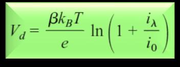
5 To evaluate current: Another relation: I V relation for semiconductor diode for no light absorption When light is absorbed an additional negative current : fraction of incident photons that absorbed to create electron hole pairs.
6 total circuit current Diode current i and voltage V d must satisfy both Eq.(14-1) and (14-3) simultaneously load-line analysis
7 Depending on application each modes have advantages and disadvantages. One important application utilizing photovoltaic mode is solar cell. Electrical power supplied to load resistor: Where practical conditions of solar illumination
8 EXAMPLE 14-1: A silicon solar cell has an area of4 cm 2, reverse saturation current density A/cm 2, and diode ideality factor β = 1. Assume that light of intensity I = 1000 W/m 2 and average wavelength500nm is incident on the cell, and that 80% of the light is absorbed. Determine optimum load resistance and power conversion efficiency. Repeat calculation for β = 2. Solution: Power striking cell Photocurrent For room temperature (20 C = 293 K)

9 For a particular value of R, solved numerically, and efficiency By varying R, graph in Fig obtained. optimum efficiency: 8.94% for R = 2.5. optimum efficiency: 17.9% for R = 5.

10 14-2. OUTPUT SATURATION In this section, examine linearity of photodiode detector circuits using two types of biasing modes Photovoltaic Mode When R is very large

11 If Where For Defining
12 Photodiode can be modeled Higher values of R sh are generally desirable, because detector is then more sensitive to weak light signals For a typical room-temperature siliconphotodiode with 1 cm 2 area, R sh 10 MΩ.

13 Summarize response of open-circuit photodiode to varying optical powers: 1. At low incident power levels responseis linearwith power 2. At high power levels response becomes logarithmic. Deviationfrom linearity at high optical powers saturationof output signal. To increaserange linearity R L can be made small. Analytically conclusion: If for photovoltaic mode
14 Equations in terms of equivalent circuit
15 When Defining Easier to measure a larger voltage, so a larger R L is desirable However, as R L is increased, one of two conditions eventually break down

16 One possibility breaks down Sameresult obtained for open-circuit condition Although V out is no longer linear with R L, it is still linear with P in. Other possibility breaks down V out is no longer linear with either R L or P in. Saturation will occur at a certain value of product P in.r L.
17 Therefore, a trade-off between sensitivity and dynamic range Saturation with incident power for different values of load resistance

18 Photoconductive Mode Saturation behavior by referring to the load-line analysis of Fig.14-3.

19 Simple analytical expression for detector signal in linear regime From Fig V d < 0 in linear regime. Good approximation

20 Detector output have two components One proportionalto incident optical power Other independent of power. Component varies with P in is identical to expression obtained for photovoltaic mode Responsivity of detector Then output in photoconductive mode

21 According to Eq. (14-17), Change in output voltage is linear with both R L and P in. However, this relation will only hold as long as V d < 0, which requires V out < V B If P in increased above point V out V B output saturates, and becomes approximately independentof P in.
22 Differences between photoconductive and photovoltaic modes 1. Saturationoccurs at V out V B in photoconductive mode, but at only V out V T in photovoltaic mode. This, improveddynamic range in photoconductive mode. 2. Photoconductive mode has a dark current, whereas photovoltaic mode does not Two consequencespresence of dark current : 1. First, it contributes a constant background level that must be subtracted from detector output to obtain true signal. 2. Second, it contributes shot noise to detector output
23 If Then both of these effects become unimportant. In this large-signal regime, photoconductive mode is best choice for detector circuit. If Then shot noise from dark current can become a dominant source of detector noise. In this small-signal regime, photovoltaic mode is a better choice.
24 14-3. RESPONSE TIME Time takes for detector output to change in response to changes in input light intensity. In photoconductive-type detectors Response time is quite poor because of electron replenishment process In photodiode detectors Replenishment process is suppressed by p n junction, which presents a barrier to movement of majority carriers. Therefore response time is significantly improved In this section, consider implications and relative importance of transit time and capacitance in determining photodiode response time.

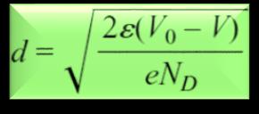
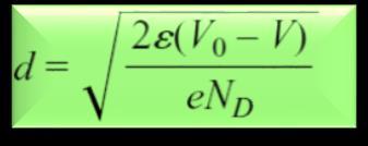
25 Junction Capacitance Evaluated by determining how charge on either side of junction changes in response to a changing diode voltage. assume junction width d When an external voltage V applied to diode
26 For reverse-bias voltage
27 If incident power suddenly switched from zero to constant value at t = 0 RC: time constant of circuit Units: seconds with R in ohms and C in farads. rise time: time taken to rise from 10% to 90% of final value. For RC circuit:
 inherently fasterthan photovoltaic mode (V B =0) 2. decreasejunction area A. give a faster time response. 3.")
28 3 db electrical bandwidth as B Results show smallercapacitancelead to faster time response and larger bandwidth Several parametersto reduce capacitance 1. Increase reverse-bias voltage V B makes photoconductive mode (V B > 0) inherently fasterthan photovoltaic mode (V B =0) 2. decreasejunction area A. give a faster time response. 3.N D is made smaller, because junction width d then increases.
29 Reducing capacitance is one way to reduce RC time constant. ReducingR L has same effect, although decreases detector sensitivity summarize various trade-offs

30 Carrier Transit Time Single p n Junction Current pulse from a single photoexcited electron lasts as long as electron moving through a region with high electric field. Since E field is high only in depletion region current pulse last a time known as transit time: d: width of depletion region v: velocity of charge carrier
31 Appear higher E field gives shorter transit time. However, dincreases with increasing E, and tends to increase transit time. To see how these two effects offset each other: Higher N D appear best for fast time response. However, junction capacitanceincreasewith higher N D, result slower response Therefore time response will be optimized when contributions.
32 EXAMPLE 14-2 A p + n silicon photodiode has an junction areaof 1mm 2, and a reverse bias of 10 V is applied through a 10 k load resistor. Determine doping levelin lightly doped n region that minimizesthe response time, and determine junction width for this doping level. Take holemobilityin Si to be m 2 /Vs. Solution: Optimumtime response occur when capacitance rise time 2.2R L Cis approximately equal to transit time t tr.
33
34 14-4. TYPES OF PHOTODIODES PIN Photodiode Assumed that photoexcited electron hole pairs created in depletion region, where there is a strong E field. This is not always the case:
35 Solution: Eliminate diffusion region. By decreasing donor concentration in n region. Middle region is very lightly doped PIN photodiode most commonly used photon detector: - Eliminates carrier diffusion, - d is fixed by geometry of device
36 EXAMPLE 14-3 A silicon PIN photodiode has an intrinsicregion of thickness 0.1 mm. Determine the minimum rise time for the detector, its corresponding bandwidth, and the required reverse-bias voltage. Repeat for an intrinsic region of thickness of 10 μm. Solution: Repeating for d = 10 μm:
 is 32%.")
37 EXAMPLE 14-4 For the silicon PIN photodiodes of Example14-3, determine the absorptionefficiency for 860 nm light. At this wavelength, the absorption coefficient in silicon is 335cm 1 and the reflectivity (from air) is 32%. Solution: Thinner intrinsic region be less efficient at absorbing incident light. Therefore, a trade-off between detector speed and sensitivity.
38 Avalanche Photodiode To increase signal generated by detector, before amplification. One way is through avalanche multiplication process:

39 Creation of electron hole pairs by impact ionization in terms of energy band:
40 A photodiode utilizing avalanche multiplication to achieve gain is termed an avalanche photodiode or APD: Structure of APD, differs from PIN: 1. light enters through a highly doped n-type layer rather than a p-type layer. 2. additional p-type layer added between highly doped n layer and intrinsic layer. Operation of APD :
 and bias voltage (magnitudes only): As bias voltage increases, area under E(x) curve increases")
41 Multiplication factor M: Ratio of photocurrent with amplification to photocurrent without amplification Relation between E(x) and bias voltage (magnitudes only): As bias voltage increases, area under E(x) curve increases proportionately.
42 At some critical voltage, depletion region reaches through to highly doped p+ region, with electric field extending uniformly through out intrinsic region. Device biased in this way is termed a reach-through APD. Typical variation of responsivity with applied bias voltage for a reach-through APD.
43 Schottky Photodiode utilizes metal semiconductor junction to separate and collect photogenerated charge carriers. operation of a Schottky photodiode for metal n n+ configuration,
44 some advantages of Schottky photodiodes over PIN photodiodes: 1. Only one metal semiconductor connection needs to be made (metal n+), and ohmic contacts are readily formed for such a junction. 2. Improved time response. 3. Metal junctions can be made with a wide variety of semiconductors, including those with wide band gap Eg, such as SiC, GaN, and AlGaN. some disadvantages of Schottky photodiodes: Less efficient than PIN photodiodes at longer wavelengths, due to reflection and absorption of light in metal layer.
45 14-5. SIGNAL-TO-NOISE RATIO signal-to-noise ratio (SNR): Ratio of electrical signal power to electrical noise power. Electrical signal power Note: Applies only when detector circuit is well below saturation. In photoconductive mode signal current defined as measured current minus dark current.
46 For shot noise For thermal noise we can write:
47 limiting cases one source of noise dominates: Large signal When, and (recall ) Noise is dominated by shot noise from signal current SNR is independent of load resistance. SNR is roughly number of charge carriers produced during measurement time. SNR increases linearly with incident optical power.
48 2. Small signal, large RL. When and SNR is limited by shot noise from dark current i0, SNR is independent of load resistance SNR increases with square of incident optical power. 3. Small signal, small RL. When and SNR is limited by thermal noise from load resistor RL.


49 noise equivalent power (NEP): Optical power that gives SNR = 1 In limiting case #2 : MKS unit for NEP is watts An alternative unit for optical power is dbm: Power in db relative to 1 mw.

50 wavelength dependence of D*
51 14-6. DETECTOR CIRCUITS High-Impedance Amplifier 3 db electrical bandwidth:
52 TransimpedanceAmplifier When response time is important, convert photocurrent iλ directly into an output voltage, bandwidth

53
Detectors for Optical Communications
 Optical Communications: Circuits, Systems and Devices Chapter 3: Optical Devices for Optical Communications lecturer: Dr. Ali Fotowat Ahmady Sep 2012 Sharif University of Technology 1 Photo All detectors
Optical Receivers Theory and Operation
 Optical Receivers Theory and Operation Photo Detectors Optical receivers convert optical signal (light) to electrical signal (current/voltage) Hence referred O/E Converter Photodetector is the fundamental
Photodiode: LECTURE-5
 LECTURE-5 Photodiode: Photodiode consists of an intrinsic semiconductor sandwiched between two heavily doped p-type and n-type semiconductors as shown in Fig. 3.2.2. Sufficient reverse voltage is applied
Optical Fiber Communication Lecture 11 Detectors
 Optical Fiber Communication Lecture 11 Detectors Warriors of the Net Detector Technologies MSM (Metal Semiconductor Metal) PIN Layer Structure Semiinsulating GaAs Contact InGaAsP p 5x10 18 Absorption InGaAs
Figure Responsivity (A/W) Figure E E-09.
 Figure E E-09.") OSI Optoelectronics, is a leading manufacturer of fiber optic components for communication systems. The products offer range for Silicon, GaAs and InGaAs to full turnkey solutions. Photodiodes are semiconductor
OSI Optoelectronics, is a leading manufacturer of fiber optic components for communication systems. The products offer range for Silicon, GaAs and InGaAs to full turnkey solutions. Photodiodes are semiconductor
Lecture 18: Photodetectors
 Lecture 18: Photodetectors Contents 1 Introduction 1 2 Photodetector principle 2 3 Photoconductor 4 4 Photodiodes 6 4.1 Heterojunction photodiode.................... 8 4.2 Metal-semiconductor photodiode................
Figure Figure E E-09. Dark Current (A) 1.
 1.") OSI Optoelectronics, is a leading manufacturer of fiber optic components for communication systems. The products offer range for Silicon, GaAs and InGaAs to full turnkey solutions. Photodiodes are semiconductor
OSI Optoelectronics, is a leading manufacturer of fiber optic components for communication systems. The products offer range for Silicon, GaAs and InGaAs to full turnkey solutions. Photodiodes are semiconductor
Optical Communications
 Optical Communications Telecommunication Engineering School of Engineering University of Rome La Sapienza Rome, Italy 2005-2006 Lecture #4, May 9 2006 Receivers OVERVIEW Photodetector types: Photodiodes
Optical Amplifiers. Continued. Photonic Network By Dr. M H Zaidi
 Optical Amplifiers Continued EDFA Multi Stage Designs 1st Active Stage Co-pumped 2nd Active Stage Counter-pumped Input Signal Er 3+ Doped Fiber Er 3+ Doped Fiber Output Signal Optical Isolator Optical
Key Questions ECE 340 Lecture 28 : Photodiodes
 Things you should know when you leave Key Questions ECE 340 Lecture 28 : Photodiodes Class Outline: How do the I-V characteristics change with illumination? How do solar cells operate? How do photodiodes
Lecture 9 External Modulators and Detectors
 Optical Fibres and Telecommunications Lecture 9 External Modulators and Detectors Introduction Where are we? A look at some real laser diodes. External modulators Mach-Zender Electro-absorption modulators
UNIT III. By Ajay Kumar Gautam Asst. Prof. Electronics & Communication Engineering Dev Bhoomi Institute of Technology & Engineering, Dehradun
 UNIT III By Ajay Kumar Gautam Asst. Prof. Electronics & Communication Engineering Dev Bhoomi Institute of Technology & Engineering, Dehradun SYLLABUS Optical Absorption in semiconductors, Types of Photo
Fundamentals of CMOS Image Sensors
 CHAPTER 2 Fundamentals of CMOS Image Sensors Mixed-Signal IC Design for Image Sensor 2-1 Outline Photoelectric Effect Photodetectors CMOS Image Sensor(CIS) Array Architecture CIS Peripherals Design Considerations
Lecture 14: Photodiodes
 Lecture 14: Photodiodes Background concepts p-n photodiodes photoconductive/photovoltaic modes p-i-n photodiodes responsivity and bandwidth Reading: Senior 8.1-8.8.3 Keiser Chapter 6 1 Electron-hole photogeneration
NON-AMPLIFIED PHOTODETECTOR USER S GUIDE
 NON-AMPLIFIED PHOTODETECTOR USER S GUIDE Thank you for purchasing your Non-amplified Photodetector. This user s guide will help answer any questions you may have regarding the safe use and optimal operation
LEDs, Photodetectors and Solar Cells
 LEDs, Photodetectors and Solar Cells Chapter 7 (Parker) ELEC 424 John Peeples Why the Interest in Photons? Answer: Momentum and Radiation High electrical current density destroys minute polysilicon and
OPTOELECTRONIC and PHOTOVOLTAIC DEVICES
 OPTOELECTRONIC and PHOTOVOLTAIC DEVICES Outline 1. Introduction to the (semiconductor) physics: energy bands, charge carriers, semiconductors, p-n junction, materials, etc. 2. Light emitting diodes Light
OFCS OPTICAL DETECTORS 11/9/2014 LECTURES 1
 OFCS OPTICAL DETECTORS 11/9/2014 LECTURES 1 1-Defintion & Mechanisms of photodetection It is a device that converts the incident light into electrical current External photoelectric effect: Electrons are
FIBER OPTICS. Prof. R.K. Shevgaonkar. Department of Electrical Engineering. Indian Institute of Technology, Bombay. Lecture: 20
 FIBER OPTICS Prof. R.K. Shevgaonkar Department of Electrical Engineering Indian Institute of Technology, Bombay Lecture: 20 Photo-Detectors and Detector Noise Fiber Optics, Prof. R.K. Shevgaonkar, Dept.
Photodiode Characteristics and Applications
 Photodiode Characteristics and Applications Silicon photodiodes are semiconductor devices responsive to highenergy particles and photons. Photodiodes operate by absorption of photons or charged particles
14.2 Photodiodes 411
 14.2 Photodiodes 411 Maximum reverse voltage is specified for Ge and Si photodiodes and photoconductive cells. Exceeding this voltage can cause the breakdown and severe deterioration of the sensor s performance.
NON-AMPLIFIED HIGH SPEED PHOTODETECTOR USER S GUIDE
 NON-AMPLIFIED HIGH SPEED PHOTODETECTOR USER S GUIDE Thank you for purchasing your Non-amplified High Speed Photodetector. This user s guide will help answer any questions you may have regarding the safe
Unit 2 Semiconductor Devices. Lecture_2.5 Opto-Electronic Devices
 Unit 2 Semiconductor Devices Lecture_2.5 Opto-Electronic Devices Opto-electronics Opto-electronics is the study and application of electronic devices that interact with light. Electronics (electrons) Optics
 Electronic Devices 1. Current flowing in each of the following circuits A and respectively are: (Circuit 1) (Circuit 2) 1) 1A, 2A 2) 2A, 1A 3) 4A, 2A 4) 2A, 4A 2. Among the following one statement is not
NAME: Last First Signature
 UNIVERSITY OF CALIFORNIA, BERKELEY College of Engineering Department of Electrical Engineering and Computer Sciences EE 130: IC Devices Spring 2003 FINAL EXAMINATION NAME: Last First Signature STUDENT
Investigate the characteristics of PIN Photodiodes and understand the usage of the Lightwave Analyzer component.
 PIN Photodiode 1 OBJECTIVE Investigate the characteristics of PIN Photodiodes and understand the usage of the Lightwave Analyzer component. 2 PRE-LAB In a similar way photons can be generated in a semiconductor,
Problem 4 Consider a GaAs p-n + junction LED with the following parameters at 300 K: Electron diusion coecient, D n = 25 cm 2 =s Hole diusion coecient
 Prof. Jasprit Singh Fall 2001 EECS 320 Homework 7 This homework is due on November 8. Problem 1 An optical power density of 1W/cm 2 is incident on a GaAs sample. The photon energy is 2.0 ev and there is
Objective Type Questions 1. Why pure semiconductors are insulators at 0 o K? 2. What is effect of temperature on barrier voltage? 3.
 Objective Type Questions 1. Why pure semiconductors are insulators at 0 o K? 2. What is effect of temperature on barrier voltage? 3. What is difference between electron and hole? 4. Why electrons have
UNIT IX ELECTRONIC DEVICES
 UNT X ELECTRONC DECES Weightage Marks : 07 Semiconductors Semiconductors diode-- characteristics in forward and reverse bias, diode as rectifier. - characteristics of LED, Photodiodes, solarcell and Zener
Lab VIII Photodetectors ECE 476
 Lab VIII Photodetectors ECE 476 I. Purpose The electrical and optical properties of various photodetectors will be investigated. II. Background Photodiode A photodiode is a standard diode packaged so that
HIGH SPEED FIBER PHOTODETECTOR USER S GUIDE
 HIGH SPEED FIBER PHOTODETECTOR USER S GUIDE Thank you for purchasing your High Speed Fiber Photodetector. This user s guide will help answer any questions you may have regarding the safe use and optimal
Università degli Studi di Roma Tor Vergata Dipartimento di Ingegneria Elettronica. Analogue Electronics. Paolo Colantonio A.A.
 Università degli Studi di Roma Tor Vergata Dipartimento di Ingegneria Elettronica Analogue Electronics Paolo Colantonio A.A. 2015-16 Introduction: materials Conductors e.g. copper or aluminum have a cloud
Avalanche Photodiode. Instructor: Prof. Dietmar Knipp Presentation by Peter Egyinam. 4/19/2005 Photonics and Optical communicaton
 Avalanche Photodiode Instructor: Prof. Dietmar Knipp Presentation by Peter Egyinam 1 Outline Background of Photodiodes General Purpose of Photodiodes Basic operation of p-n, p-i-n and avalanche photodiodes
2nd Asian Physics Olympiad
 2nd Asian Physics Olympiad TAIPEI, TAIWAN Experimental Competition Thursday, April 26, 21 Time Available : 5 hours Read This First: 1. Use only the pen provided. 2. Use only the front side of the answer
10/27/2009 Reading: Chapter 10 of Hambley Basic Device Physics Handout (optional)
") EE40 Lec 17 PN Junctions Prof. Nathan Cheung 10/27/2009 Reading: Chapter 10 of Hambley Basic Device Physics Handout (optional) Slide 1 PN Junctions Semiconductor Physics of pn junctions (for reference
EE40 Lec 17 PN Junctions Prof. Nathan Cheung 10/27/2009 Reading: Chapter 10 of Hambley Basic Device Physics Handout (optional) Slide 1 PN Junctions Semiconductor Physics of pn junctions (for reference
UNIT 3: FIELD EFFECT TRANSISTORS
 FIELD EFFECT TRANSISTOR: UNIT 3: FIELD EFFECT TRANSISTORS The field effect transistor is a semiconductor device, which depends for its operation on the control of current by an electric field. There are
Department of Electrical Engineering IIT Madras
 Department of Electrical Engineering IIT Madras Sample Questions on Semiconductor Devices EE3 applicants who are interested to pursue their research in microelectronics devices area (fabrication and/or
Downloaded from
 Question 14.1: In an n-type silicon, which of the following statement is true: (a) Electrons are majority carriers and trivalent atoms are the dopants. (b) Electrons are minority carriers and pentavalent
MOSFET short channel effects
 MOSFET short channel effects overview Five different short channel effects can be distinguished: velocity saturation drain induced barrier lowering (DIBL) impact ionization surface scattering hot electrons
Chapter 3 OPTICAL SOURCES AND DETECTORS
 Chapter 3 OPTICAL SOURCES AND DETECTORS 3. Optical sources and Detectors 3.1 Introduction: The success of light wave communications and optical fiber sensors is due to the result of two technological breakthroughs.
CONTENTS. 2.2 Schrodinger's Wave Equation 31. PART I Semiconductor Material Properties. 2.3 Applications of Schrodinger's Wave Equation 34
 CONTENTS Preface x Prologue Semiconductors and the Integrated Circuit xvii PART I Semiconductor Material Properties CHAPTER 1 The Crystal Structure of Solids 1 1.0 Preview 1 1.1 Semiconductor Materials
Solar-energy conversion and light emission in an atomic monolayer p n diode
 Solar-energy conversion and light emission in an atomic monolayer p n diode Andreas Pospischil, Marco M. Furchi, and Thomas Mueller 1. I-V characteristic of WSe 2 p-n junction diode in the dark The Shockley
Review Energy Bands Carrier Density & Mobility Carrier Transport Generation and Recombination
 Review Energy Bands Carrier Density & Mobility Carrier Transport Generation and Recombination Current Transport: Diffusion, Thermionic Emission & Tunneling For Diffusion current, the depletion layer is
Figure 2d. Optical Through-the-Air Communications Handbook -David A. Johnson,
 onto the detector. The stray light competes with the modulated light from the distant transmitter. If the environmental light is sufficiently strong it can interfere with light from the light transmitter.
Semiconductor Devices Lecture 5, pn-junction Diode
 Semiconductor Devices Lecture 5, pn-junction Diode Content Contact potential Space charge region, Electric Field, depletion depth Current-Voltage characteristic Depletion layer capacitance Diffusion capacitance
Section 2.3 Bipolar junction transistors - BJTs
 Section 2.3 Bipolar junction transistors - BJTs Single junction devices, such as p-n and Schottkty diodes can be used to obtain rectifying I-V characteristics, and to form electronic switching circuits
Introduction to Photovoltaics
 Introduction to Photovoltaics PHYS 4400, Principles and Varieties of Solar Energy Instructor: Randy J. Ellingson The University of Toledo February 24, 2015 Only solar energy Of all the possible sources
LOGARITHMIC PROCESSING APPLIED TO NETWORK POWER MONITORING
 ARITHMIC PROCESSING APPLIED TO NETWORK POWER MONITORING Eric J Newman Sr. Applications Engineer in the Advanced Linear Products Division, Analog Devices, Inc., email: eric.newman@analog.com Optical power
Photons and solid state detection
 Photons and solid state detection Photons represent discrete packets ( quanta ) of optical energy Energy is hc/! (h: Planck s constant, c: speed of light,! : wavelength) For solid state detection, photons
ECEN 4606, UNDERGRADUATE OPTICS LAB
 ECEN 4606, UNDERGRADUATE OPTICS LAB Lab 10: Photodetectors Original: Professor McLeod SUMMARY: In this lab, you will characterize the fundamental low-frequency characteristics of photodiodes and the circuits
Solar Cell Parameters and Equivalent Circuit
 9 Solar Cell Parameters and Equivalent Circuit 9.1 External solar cell parameters The main parameters that are used to characterise the performance of solar cells are the peak power P max, the short-circuit
Amplified Photodetectors
 Amplified Photodetectors User Guide (800)697-6782 sales@eotech.com www.eotech.com Page 1 of 6 EOT AMPLIFIED PHOTODETECTOR USER S GUIDE Thank you for purchasing your Amplified Photodetector from EOT. This
Ultra-sensitive SiGe Bipolar Phototransistors for Optical Interconnects
 Ultra-sensitive SiGe Bipolar Phototransistors for Optical Interconnects Michael Roe Electrical Engineering and Computer Sciences University of California at Berkeley Technical Report No. UCB/EECS-2012-123
THE METAL-SEMICONDUCTOR CONTACT
 THE METAL-SEMICONDUCTOR CONTACT PROBLEM 1 To calculate the theoretical barrier height, built-in potential barrier, and maximum electric field in a metal-semiconductor diode for zero applied bias. Consider
Copyright -International Centre for Diffraction Data 2010 ISSN
 234 BRIDGING THE PRICE/PERFORMANCE GAP BETWEEN SILICON DRIFT AND SILICON PIN DIODE DETECTORS Derek Hullinger, Keith Decker, Jerry Smith, Chris Carter Moxtek, Inc. ABSTRACT Use of silicon drift detectors
Amplified High Speed Photodetectors
 Amplified High Speed Photodetectors User Guide 3340 Parkland Ct. Traverse City, MI 49686 USA Page 1 of 6 Thank you for purchasing your Amplified High Speed Photodetector from EOT. This user guide will
Non-amplified Photodetectors
 Non-amplified Photodetectors User Guide (800)697-6782 sales@eotech.com www.eotech.com Page 1 of 9 EOT NON-AMPLIFIED PHOTODETECTOR USER S GUIDE Thank you for purchasing your Non-amplified Photodetector
Module 10 : Receiver Noise and Bit Error Ratio
 Module 10 : Receiver Noise and Bit Error Ratio Lecture : Receiver Noise and Bit Error Ratio Objectives In this lecture you will learn the following Receiver Noise and Bit Error Ratio Shot Noise Thermal
Lecture 8 Optical Sensing. ECE 5900/6900 Fundamentals of Sensor Design
 ECE 5900/6900: Fundamentals of Sensor Design Lecture 8 Optical Sensing 1 Optical Sensing Q: What are we measuring? A: Electromagnetic radiation labeled as Ultraviolet (UV), visible, or near,mid-, far-infrared
What is the highest efficiency Solar Cell?
 What is the highest efficiency Solar Cell? GT CRC Roof-Mounted PV System Largest single PV structure at the time of it s construction for the 1996 Olympic games Produced more than 1 billion watt hrs. of
Lecture 9: Limiting and Clamping Diode Circuits. Voltage Doubler. Special Diode Types.
 Whites, EE 320 Lecture 9 Page 1 of 8 Lecture 9: Limiting and Clamping Diode Circuits. Voltage Doubler. Special Diode Types. We ll finish up our discussion of diodes in this lecture by consider a few more
Photon Count. for Brainies.
 Page 1/12 Photon Count ounting for Brainies. 0. Preamble This document gives a general overview on InGaAs/InP, APD-based photon counting at telecom wavelengths. In common language, telecom wavelengths
Silicon Avalanche Photodetectors Fabricated With Standard CMOS/BiCMOS Technology Myung-Jae Lee
 Silicon Avalanche Photodetectors Fabricated With Standard CMOS/BiCMOS Technology Myung-Jae Lee The Graduate School Yonsei University Department of Electrical and Electronic Engineering Silicon Avalanche
QUANTUM EFFICIENCY (Q.E)
") 31 I נספח 1: אופייני פוטודיודות SPETAL ESPONSE The photocurrent produced by a given level of incident light varies with wavelength This wavelength/ response relationship is known as the spectral response
31 I נספח 1: אופייני פוטודיודות SPETAL ESPONSE The photocurrent produced by a given level of incident light varies with wavelength This wavelength/ response relationship is known as the spectral response
Measure the roll-off frequency of an acousto-optic modulator
 Slide 1 Goals of the Lab: Get to know some of the properties of pin photodiodes Measure the roll-off frequency of an acousto-optic modulator Measure the cut-off frequency of a pin photodiode as a function
A silicon avalanche photodetector fabricated with standard CMOS technology with over 1 THz gain-bandwidth product
 A silicon avalanche photodetector fabricated with standard CMOS technology with over 1 THz gain-bandwidth product Myung-Jae Lee and Woo-Young Choi* Department of Electrical and Electronic Engineering,
Fundamentals of Power Semiconductor Devices
 В. Jayant Baliga Fundamentals of Power Semiconductor Devices 4y Spri ringer Contents Preface vii Chapter 1 Introduction 1 1.1 Ideal and Typical Power Switching Waveforms 3 1.2 Ideal and Typical Power Device
Physics of Waveguide Photodetectors with Integrated Amplification
 Physics of Waveguide Photodetectors with Integrated Amplification J. Piprek, D. Lasaosa, D. Pasquariello, and J. E. Bowers Electrical and Computer Engineering Department University of California, Santa
Difference between BJTs and FETs. Junction Field Effect Transistors (JFET)
") Difference between BJTs and FETs Transistors can be categorized according to their structure, and two of the more commonly known transistor structures, are the BJT and FET. The comparison between BJTs
Difference between BJTs and FETs Transistors can be categorized according to their structure, and two of the more commonly known transistor structures, are the BJT and FET. The comparison between BJTs
SRM INSTITUTE OF SCIENCE AND TECHNOLOGY (DEEMED UNIVERSITY)
") SRM INSTITUTE OF SCIENCE AND TECHNOLOGY (DEEMED UNIVERSITY) QUESTION BANK I YEAR B.Tech (II Semester) ELECTRONIC DEVICES (COMMON FOR EC102, EE104, IC108, BM106) UNIT-I PART-A 1. What are intrinsic and
SRM INSTITUTE OF SCIENCE AND TECHNOLOGY (DEEMED UNIVERSITY) QUESTION BANK I YEAR B.Tech (II Semester) ELECTRONIC DEVICES (COMMON FOR EC102, EE104, IC108, BM106) UNIT-I PART-A 1. What are intrinsic and
Section:A Very short answer question
 Section:A Very short answer question 1.What is the order of energy gap in a conductor, semi conductor, and insulator?. Conductor - no energy gap Semi Conductor - It is of the order of 1 ev. Insulator -
Chapter 16 Other Two-Terminal Devices
 Chapter 16 Other Two-Terminal Devices 1 Other Two-Terminal Terminal Devices Schottky diode Varactor diode Power diodes Tunnel diode Photodiode Photoconductive cells IR emitters Liquid crystal displays
Chapter 8. Field Effect Transistor
 Chapter 8. Field Effect Transistor Field Effect Transistor: The field effect transistor is a semiconductor device, which depends for its operation on the control of current by an electric field. There
Prepared by: Dr. Rishi Prakash, Dept of Electronics and Communication Engineering Page 1 of 5
 Microwave tunnel diode Some anomalous phenomena were observed in diode which do not follows the classical diode equation. This anomalous phenomena was explained by quantum tunnelling theory. The tunnelling
LAB V. LIGHT EMITTING DIODES
 LAB V. LIGHT EMITTING DIODES 1. OBJECTIVE In this lab you will measure the I-V characteristics of Infrared (IR), Red and Blue light emitting diodes (LEDs). Using a photodetector, the emission intensity
Electronic devices-i. Difference between conductors, insulators and semiconductors
 Electronic devices-i Semiconductor Devices is one of the important and easy units in class XII CBSE Physics syllabus. It is easy to understand and learn. Generally the questions asked are simple. The unit
EEE118: Electronic Devices and Circuits
 EEE118: Electronic Devices and Circuits Lecture IIII James E Green Department of Electronic Engineering University of Sheffield j.e.green@sheffield.ac.uk Last Lecture: Review 1 Defined some terminology
SUPPLEMENTARY INFORMATION
 DOI: 1.138/NPHOTON.212.11 Supplementary information Avalanche amplification of a single exciton in a semiconductor nanowire Gabriele Bulgarini, 1, Michael E. Reimer, 1, Moïra Hocevar, 1 Erik P.A.M. Bakkers,
 Energy band diagrams Metals: 9. ELECTRONIC DEVICES GIST ρ= 10-2 to 10-8 Ω m Insulators: ρ> 10 8 Ω m Semiconductors ρ= 1 to 10 5 Ω m 109 A. Intrinsic semiconductors At T=0k it acts as insulator At room
LAB V. LIGHT EMITTING DIODES
 LAB V. LIGHT EMITTING DIODES 1. OBJECTIVE In this lab you are to measure I-V characteristics of Infrared (IR), Red and Blue light emitting diodes (LEDs). The emission intensity as a function of the diode
Physics and Technology
 Physics and Technology Emitters Materials Infrared emitting diodes (IREDs) can be produced from a range of different III-V compounds. Unlike the elemental semiconductor silicon, the compound III-V semiconductors
Opto-electronic Receivers
 Purpose of a Receiver The receiver fulfils the function of optoelectronic conversion of an input optical signal into an output electrical signal (data stream). The purpose is to recover the data transmitted
CMOS Phototransistors for Deep Penetrating Light
 CMOS Phototransistors for Deep Penetrating Light P. Kostov, W. Gaberl, H. Zimmermann Institute of Electrodynamics, Microwave and Circuit Engineering, Vienna University of Technology Gusshausstr. 25/354,
Modelling and Analysis of Four-Junction Tendem Solar Cell in Different Environmental Conditions Mr. Biraju J. Trivedi 1 Prof. Surendra Kumar Sriwas 2
 IJSRD - International Journal for Scientific Research & Development Vol. 3, Issue 08, 2015 ISSN (online): 2321-0613 Modelling and Analysis of Four-Junction Tendem Solar Cell in Different Environmental
Instruction manual and data sheet ipca h
 1/15 instruction manual ipca-21-05-1000-800-h Instruction manual and data sheet ipca-21-05-1000-800-h Broad area interdigital photoconductive THz antenna with microlens array and hyperhemispherical silicon
Digital Integrated Circuits A Design Perspective. The Devices. Digital Integrated Circuits 2nd Devices
 Digital Integrated Circuits A Design Perspective The Devices The Diode The diodes are rarely explicitly used in modern integrated circuits However, a MOS transistor contains at least two reverse biased
Recent Development and Study of Silicon Solid State Photomultiplier (MRS Avalanche Photodetector)
") Recent Development and Study of Silicon Solid State Photomultiplier (MRS Avalanche Photodetector) Valeri Saveliev University of Obninsk, Russia Vienna Conference on Instrumentation Vienna, 20 February
Recent Development and Study of Silicon Solid State Photomultiplier (MRS Avalanche Photodetector) Valeri Saveliev University of Obninsk, Russia Vienna Conference on Instrumentation Vienna, 20 February
Study and Measurement of the Main Parameters of a Laser quadrant Detector
 Cairo University National Institute of Laser Enhanced Sciences Laser Sciences and Interactions Study and Measurement of the Main Parameters of a Laser quadrant Detector By Eng. Mohamed Abd-Elfattah Abd-Elazim
Non-amplified High Speed Photodetectors
 Non-amplified High Speed Photodetectors User Guide (800)697-6782 sales@eotech.com www.eotech.com Page 1 of 6 EOT NON-AMPLIFIED HIGH SPEED PHOTODETECTOR USER S GUIDE Thank you for purchasing your Non-amplified
UNIT VIII-SPECIAL PURPOSE ELECTRONIC DEVICES. 1. Explain tunnel Diode operation with the help of energy band diagrams.
 UNIT III-SPECIAL PURPOSE ELECTRONIC DEICES 1. Explain tunnel Diode operation with the help of energy band diagrams. TUNNEL DIODE: A tunnel diode or Esaki diode is a type of semiconductor diode which is
P-N Diodes & Applications
 P-N Diodes & Applications Outline Major junction diode applications are Electronics circuit control Rectifying (forward mode) Special break-down diodes: Zener and avalanche Switching Circuit tuning (varactor)
Basic Electronics Important questions
 Basic Electronics Important questions B.E-2/4 Mech- B Faculty: P.Lakshmi Prasanna Note: Read the questions in the following order i. Assignment questions ii. Class test iii. Expected questions iv. Tutorials
Lecture 4 -- Tuesday, Sept. 19: Non-uniform injection and/or doping. Diffusion. Continuity/conservation. The five basic equations.
 6.012 ELECTRONIC DEVICES AND CIRCUITS Schedule -- Fall 1995 (8/31/95 version) Recitation 1 -- Wednesday, Sept. 6: Review of 6.002 models for BJT. Discussion of models and modeling; motivate need to go
Unit III FET and its Applications. 2 Marks Questions and Answers
 Unit III FET and its Applications 2 Marks Questions and Answers 1. Why do you call FET as field effect transistor? The name field effect is derived from the fact that the current is controlled by an electric
UNIT-III SOURCES AND DETECTORS. According to the shape of the band gap as a function of the momentum, semiconductors are classified as
 UNIT-III SOURCES AND DETECTORS DIRECT AND INDIRECT BAND GAP SEMICONDUCTORS: According to the shape of the band gap as a function of the momentum, semiconductors are classified as 1. Direct band gap semiconductors
Choosing and Using Photo Sensors
 Part II Choosing and Using Photo Sensors Selection of the right photo sensor is the first step towards designing an optimal sensor-based system. The second step, and indeed a very important one, is the
Development of High Sensitivity SWIR APD Receivers
 Development of High Sensitivity SWIR APD Receivers Xiaogang Bai* a, Ping Yuan a, James Chang a, Rengarajan Sudharsanan a, Michael Krainak b, Guangning Yang b, Xiaoli Sun b, Wei Lu b, a Spectrolab Inc.,
Chapter 1: Semiconductor Diodes
 Chapter 1: Semiconductor Diodes Diodes The diode is a 2-terminal device. A diode ideally conducts in only one direction. 2 Diode Characteristics Conduction Region Non-Conduction Region The voltage across
OPTI510R: Photonics. Khanh Kieu College of Optical Sciences, University of Arizona Meinel building R.626
 OPTI510R: Photonics Khanh Kieu College of Optical Sciences, University of Arizona kkieu@optics.arizona.edu Meinel building R.626 Photodetectors Introduction Most important characteristics Photodetector
1 Semiconductor-Photon Interaction
 1 SEMICONDUCTOR-PHOTON INTERACTION 1 1 Semiconductor-Photon Interaction Absorption: photo-detectors, solar cells, radiation sensors. Radiative transitions: light emitting diodes, displays. Stimulated emission: