Moderne Teilchendetektoren - Theorie und Praxis 2. Dr. Bernhard Ketzer Technische Universität München SS 2013
|
|
|
- Piers Edwards
- 6 years ago
- Views:
Transcription
1 Moderne Teilchendetektoren - Theorie und Praxis 2 Dr. Bernhard Ketzer Technische Universität München SS 2013
2 7 Signal Processing and Acquisition 7.1 Signals 7.2 Amplifier 7.3 Electronic Noise 7.4 Analog-to-Digital Conversion 7.5 Time-to-Digital Conversion 7.6 Trigger 7.7 Data Readout and Acquisition
3 Overview General scheme of a measurement system: 1. Radiation deposits energy in a detecting medium 2. Energy is converted into an electric signal direct conversion: ionization ionization chamber: e -ion pairs semiconductor detector: e -hole pairs indirect conversion: excitation emission of light conversion into charge scintillation detectors primary signal charge absorbed energy Energy required per e ~ 30 ev ~ 3 ev ~ 300 ev
4 Overview 3. Signal amplitude small amplification necessary secondary amplification proportional counter photomultiplier tube avalanche photodiode electronic circuit introduction of random fluctuations (noise) 4. Pulse shaping, e.g. [H. Spieler, Semiconductor Detector Systems, Oxford 2005]
5 Overview 5. Digitization extraction of information detector channel position signal amplitude energy time 6. Based on this information decision to keep or discard the event store data read other detectors reset / clear information Trigger
6 Overview Example: [H. Spieler, Semiconductor Detector Systems, Oxford 2005]
7 7.1 Signals
8 7.1.1 Fluctuations in Signal Charge Consider Si detector: average number of e -hole pairs average energy loss average energy required per e -hole pair Two limiting cases: Only a very small fraction E 0 of the total energy E of the incident particle is converted into e -hole pairs statistically independent processes Poisson statistics (i.e. energy loss can vary within Poisson statistics)
9 Fluctuations in Signal Charge Total energy of incident particle is converted into e -hole pairs (no other process of energy dissipation!) no fluctuations (i.e. each particle of the same total energy will create the same number of e -hole pairs) Real detector: Fano factor, Si: processes for creation of single charge carriers statistically not independent (fixed value of energy deposition) in solids: electronic excitation in connection with lattice excitation (phonons)
10 Fluctuations in Signal Charge Fano factor determined by all fundamental processes for energy dissipation in the detector, including non-ionizing ones depends on material difficult to calculate from first principles mostly: empirical values Further source of fluctuations: electronic noise
11 Fluctuations in Signal Charge Example: 2 types of interactions in solid lattice excitation (phonon production): N x excitations produce N p phonons ionization: N i ionizations produce N Q charge pairs sum of energies going in excitation and ionization is equal to energy E 0 deposited by incident radiation: E x = energy required for single excitation = average phonon energy in semicond. E i = energy required for single ionization = bandgap in semiconductor
 For there is always some combination of excitation and")

12 Fluctuations in Signal Charge For a single event: E 0 fixed (but can vary from event to event) For there is always some combination of excitation and ionization to dissipate exactly the deposited energy fluctuation in excitation is balanced by fluctuation in ionization Averaging over many events With
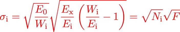
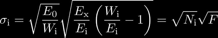
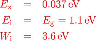
13 Fluctuations in Signal Charge With follows In Silicon: Experiment:
14 Fluctuations in Signal Charge Energy resolution: Peaks can be resolved if separation of peaks larger than their FWHM [W.R. Leo, Techniques for Nuclear and Particle Physics Experiments, Springer 1994]
15 Energy Resolution [H. Spieler, Semiconductor Detector Systems, Oxford University Press 2005]
16 7.1.2 Signal Formation Charge moving in sensitive volume of detector signal current Ramo s Theorem: [H. Spieler, Semiconductor Detector Systems, Oxford University Press 2005]
17 7.1.3 Terminology baseline pulse height, amplitude pulse width FWHM rising edge falling edge rise time fall time unipolar - bipolar [W.R. Leo, Techniques for Nuclear and Particle Physics Experiments, Springer, 1994]
18 Terminology Analog signal: continuously varying characteristics (amplitude, time, shape) e.g. proportional counter Digital signal: discretely varying, quantized property e.g. Geiger-Müller counter: yes/no normally two states: 0, 1 technically more reliable (resistant to external perturbations), but carries less information per pulse
19 Logic Elements Common logic functions: Logic symbols: [H. Spieler, Semiconductor Detector Systems, Oxford University Press 2005]
20 7.1.4 Frequency Domain, Bandwidth
21 Bandwidth Example: rectangle pulse F( ω)= ωt sin AT 2 2π ωt 2 continuous frequency spectrum!
22 Bandwidth Perfect electronic device for processing of f(t) uniform response to infinite range of frequencies Real device transmission limited to finite range in ω (R, C, L) Typ. frequency response of an electr. circuit [W.R. Leo, Techniques for Nuclear and Particle Physics Experiments, Springer, 1994]
23 Pulse Signals and Bandwidth Important: transmission of information carrying parts of signal, e.g. amplitude, rising edge Effect of limited bandwith on rectangular pulse [W.R. Leo, Techniques for Nuclear and Particle Physics Experiments, Springer, 1994] minimum bandwidth: typical bandwidths: 100 khz 1 GHz
24 7.1.5 Signal Transmission
25 Signal Transmission I(z,t) I(z+ z,t) U(z,t) U(z+ z,t)
26 Signal Transmission
27 Signal Transmission
28 Signal Transmission
29 Signal Transmission
30 Signal Transmission
31 Signal Transmission [W.R. Leo, Techniques for Nuclear and Particle Physics Experiments, Springer, 1994]
32 Signal Transmission
33 Pulse Transmission by Cable [W.R. Leo, Techniques for Nuclear and Particle Physics Experiments, Springer, 1994]
34 7.2 Amplifier Amplifies weak signals from detector Drives signal through cable Low noise close to detector
35 7.2.1 Bipolar Transistor Structure: 3 subsequent regions of different doping (npn, pnp) Example: npn transistor U C > U E > U B : both diodes BC and EB reverse biased only reverse current I C = I C (U CE ) through BC, depending on n p (minority carrier concentration) U C > U B > U E (U BE > 0): diode BE forward biased, BC reverse e - get from n+ into p-zone increase of n p = n p (U BE ) [Ibach, Lüth, Festkörperphysik, Springer, 2002]

36 Bipolar Transistor [Ibach, Lüth, Festkörperphysik, Springer, 2002]
37 Bipolar Transistor If p-zone very thin (~µm) d < λ (mean free path for recombination) e - may reach pn junction of diode BC transported into n-zone by U CE current I C = I C (U BE ) strongly non-linear most important property of transistor
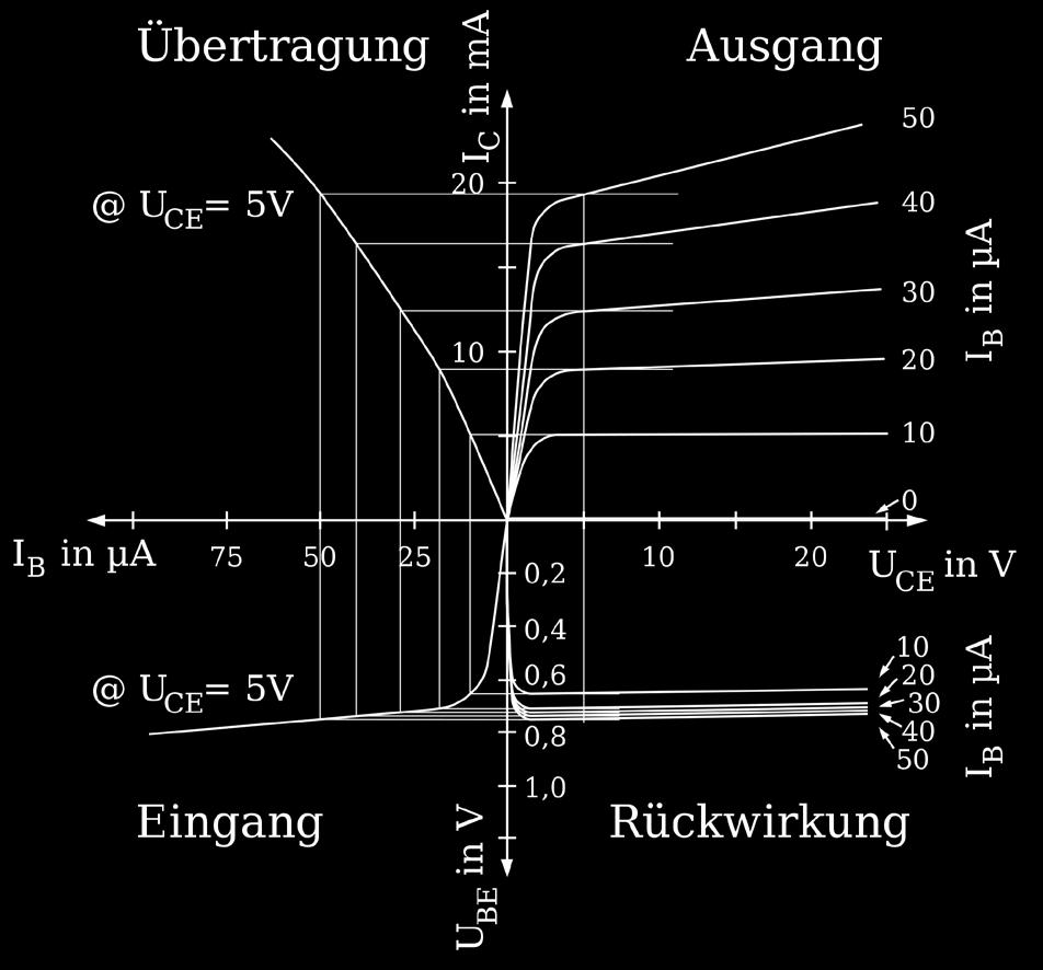
38 Bipolar Transistor Behavior of transistor described by characteristic curves, i.e. relation between currents and voltages (static situation) Common emitter circuit: Forward (active) region: application as amplifier I C I B > 0, U BE > 0, U CE U CE,sat ~ U BE BE forward, BC reverse Saturation region U BE I B I E U CE I B > 0, U BE > 0, U CE U BE BE forward, BC forward Cut-off region I B 0, U BE 0, U CE > 0 BE reverse, BC reverse application as switch Here: U BE > 0 BE forward
39 Transistor Characteristics Transmission characteristics: I C (U BE ) exponential dependence (diode) [Tietze, Schenk, Halbleiter-Schaltungstechnik, Springer, 1999]
40 Transistor Characteristics Output characteristics: I C (U CE ) Saturation region: U CE < U CE,sat BC forward I C increases strongly with U CE transistor saturates Active region: U CE > U CE,sat weak dependence of I C on U CE (finite slope: Early effect) Definition: differential output resistance (at working point A) [Tietze, Schenk, Halbleiter- Schaltungstechnik, Springer, 1999]
41 Transistor Characteristics Input characteristics: I B (U BE ) exponential dependence (diode BE) Definition: differential input resistance (at working point A) at 300 K: thermal voltage typ.: [Tietze, Schenk, Halbleiter-Schaltungstechnik, Springer, 1999]

42 Transistor Characteristics Similar dependence of I B (U BE ) and I C (U BE ) in active region Definition: small signal current gain (at working point A) In active region of transistor: [Tietze, Schenk, Halbleiter-Schaltungstechnik, Springer, 1999] i.e. small signal current gain agrees with DC current gain

43 Transistor Characteristics [
44 Transistor Circuits Rohe, Elektronik für Physiker, Teubner, 1978]
45 7.2.2 Grounded Emitter Amplifier bias voltage
46 Grounded Emitter Amplifier [A. Schlachetzki, Halbleiter-Elektronik, Teubner, 1990]

47 Grounded Emitter Amplifier
48 Grounded Emitter Amplifier
49 Grounded Emitter Amplifier
50 Grounded Emitter Amplifier Voltage amplification (w/o load): A 0 R r C = BE β 200 typ. only valid for U BE <<U T (linear relation R BE = U BE / I B ) strong distortions for U BE U T A 0 depends directly on β, r BE (vary with T and between devices) T dependence of I C at fixed U BE (diode)
51 Grounded Emitter Amplifier
Semiconductor Detector Systems
 Semiconductor Detector Systems Helmuth Spieler Physics Division, Lawrence Berkeley National Laboratory OXFORD UNIVERSITY PRESS ix CONTENTS 1 Detector systems overview 1 1.1 Sensor 2 1.2 Preamplifier 3
Analog & Digital Electronics Course No: PH-218
 Analog & Digital Electronics Course No: PH-218 Lec-5: Bipolar Junction Transistor (BJT) Course nstructors: Dr. A. P. VAJPEY Department of Physics, ndian nstitute of Technology Guwahati, ndia 1 Bipolar
Chapter 3 Bipolar Junction Transistors (BJT)
") Chapter 3 Bipolar Junction Transistors (BJT) Transistors In analog circuits, transistors are used in amplifiers and linear regulated power supplies. In digital circuits they function as electrical switches,
Chapter 3 Bipolar Junction Transistors (BJT) Transistors In analog circuits, transistors are used in amplifiers and linear regulated power supplies. In digital circuits they function as electrical switches,
Bipolar Junction Transistor (BJT)
") Bipolar Junction Transistor (BJT) - three terminal device - output port controlled by current flow into input port Structure - three layer sandwich of n-type and p-type material - npn and pnp transistors
Bipolar Junction Transistor (BJT) - three terminal device - output port controlled by current flow into input port Structure - three layer sandwich of n-type and p-type material - npn and pnp transistors
Physics of Bipolar Transistor
 Physics of Bipolar Transistor Motivations - In many electronic applications, amplifier is the most fundamental building block. Ex Audio amplifier: amplifies electric signal to drive a speaker RF Power
Lecture 24: Bipolar Junction Transistors (1) Bipolar Junction Structure, Operating Regions, Biasing
 Bipolar Junction Structure, Operating Regions, Biasing") Lecture 24: Bipolar Junction Transistors (1) Bipolar Junction Structure, Operating Regions, Biasing BJT Structure the BJT is formed by doping three semiconductor regions (emitter, base, and collector)
Lecture 24: Bipolar Junction Transistors (1) Bipolar Junction Structure, Operating Regions, Biasing BJT Structure the BJT is formed by doping three semiconductor regions (emitter, base, and collector)
An Introduction to Bipolar Junction Transistors. Prepared by Dr Yonas M Gebremichael, 2005
 An Introduction to Bipolar Junction Transistors Transistors Transistors are three port devices used in most integrated circuits such as amplifiers. Non amplifying components we have seen so far, such as
Bipolar Junction Transistors (BJTs)
") C H A P T E R 6 Bipolar Junction Transistors (BJTs) Figure 6.1 A simplified structure of the npn transistor and pnp transistor. Table 6.1: BJT modes of Operation Mode Cutoff Active Saturation EBJ Reverse
C H A P T E R 6 Bipolar Junction Transistors (BJTs) Figure 6.1 A simplified structure of the npn transistor and pnp transistor. Table 6.1: BJT modes of Operation Mode Cutoff Active Saturation EBJ Reverse
EE301 Electronics I , Fall
 EE301 Electronics I 2018-2019, Fall 1. Introduction to Microelectronics (1 Week/3 Hrs.) Introduction, Historical Background, Basic Consepts 2. Rewiev of Semiconductors (1 Week/3 Hrs.) Semiconductor materials
 Electronic Devices 1. Current flowing in each of the following circuits A and respectively are: (Circuit 1) (Circuit 2) 1) 1A, 2A 2) 2A, 1A 3) 4A, 2A 4) 2A, 4A 2. Among the following one statement is not
Downloaded from
 Question 14.1: In an n-type silicon, which of the following statement is true: (a) Electrons are majority carriers and trivalent atoms are the dopants. (b) Electrons are minority carriers and pentavalent
Bipolar Junction Transistors
 Bipolar Junction Transistors Invented in 1948 at Bell Telephone laboratories Bipolar junction transistor (BJT) - one of the major three terminal devices Three terminal devices more useful than two terminal
COE/EE152: Basic Electronics. Lecture 5. Andrew Selasi Agbemenu. Outline
 COE/EE152: Basic Electronics Lecture 5 Andrew Selasi Agbemenu 1 Outline Physical Structure of BJT Two Diode Analogy Modes of Operation Forward Active Mode of BJTs BJT Configurations Early Effect Large
EE105 Fall 2014 Microelectronic Devices and Circuits. NPN Bipolar Junction Transistor (BJT)
") EE105 Fall 2014 Microelectronic Devices and Circuits Prof. Ming C. Wu wu@eecs.berkeley.edu 511 utardja Dai Hall (DH) 1 NPN Bipolar Junction Transistor (BJT) Forward Bias Reverse Bias Hole Flow Electron
EE105 Fall 2014 Microelectronic Devices and Circuits Prof. Ming C. Wu wu@eecs.berkeley.edu 511 utardja Dai Hall (DH) 1 NPN Bipolar Junction Transistor (BJT) Forward Bias Reverse Bias Hole Flow Electron
Review Energy Bands Carrier Density & Mobility Carrier Transport Generation and Recombination
 Review Energy Bands Carrier Density & Mobility Carrier Transport Generation and Recombination Current Transport: Diffusion, Thermionic Emission & Tunneling For Diffusion current, the depletion layer is
MTLE-6120: Advanced Electronic Properties of Materials. Semiconductor transistors for logic and memory. Reading: Kasap
 MTLE-6120: Advanced Electronic Properties of Materials 1 Semiconductor transistors for logic and memory Reading: Kasap 6.6-6.8 Vacuum tube diodes 2 Thermionic emission from cathode Electrons collected
Electronic Instrumentation for Radiation Detection Systems
 Electronic Instrumentation for Radiation Detection Systems January 23, 2018 Joshua W. Cates, Ph.D. and Craig S. Levin, Ph.D. Course Outline Lecture Overview Brief Review of Radiation Detectors Detector
Characterisation of SiPM Index :
 Characterisation of SiPM --------------------------------------------------------------------------------------------Index : 1. Basics of SiPM* 2. SiPM module 3. Working principle 4. Experimental setup
Chapter 3-2 Semiconductor devices Transistors and Amplifiers-BJT Department of Mechanical Engineering
 MEMS1082 Chapter 3-2 Semiconductor devices Transistors and Amplifiers-BJT Bipolar Transistor Construction npn BJT Transistor Structure npn BJT I = I + E C I B V V BE CE = V = V B C V V E E Base-to-emitter
Figure1: Basic BJT construction.
 Chapter 4: Bipolar Junction Transistors (BJTs) Bipolar Junction Transistor (BJT) Structure The BJT is constructed with three doped semiconductor regions separated by two pn junctions, as in Figure 1(a).
Student Lecture by: Giangiacomo Groppi Joel Cassell Pierre Berthelot September 28 th 2004
 Student Lecture by: Giangiacomo Groppi Joel Cassell Pierre Berthelot September 28 th 2004 Lecture outline Historical introduction Semiconductor devices overview Bipolar Junction Transistor (BJT) Field
Bipolar Junction Transistors (BJTs) Overview
 Overview") 1 Bipolar Junction Transistors (BJTs) Asst. Prof. MONTREE SIRIPRUCHYANUN, D. Eng. Dept. of Teacher Training in Electrical Engineering, Faculty of Technical Education King Mongkut s Institute of Technology
1 Bipolar Junction Transistors (BJTs) Asst. Prof. MONTREE SIRIPRUCHYANUN, D. Eng. Dept. of Teacher Training in Electrical Engineering, Faculty of Technical Education King Mongkut s Institute of Technology
Tutors Dominik Dannheim, Thibault Frisson (CERN, Geneva, Switzerland)
") Danube School on Instrumentation in Elementary Particle & Nuclear Physics University of Novi Sad, Serbia, September 8 th 13 th, 2014 Lab Experiment: Characterization of Silicon Photomultipliers Dominik
Danube School on Instrumentation in Elementary Particle & Nuclear Physics University of Novi Sad, Serbia, September 8 th 13 th, 2014 Lab Experiment: Characterization of Silicon Photomultipliers Dominik
C H A P T E R 6 Bipolar Junction Transistors (BJTs)
") C H A P T E R 6 Bipolar Junction Transistors (BJTs) Figure 6.1 A simplified structure of the npn transistor and pnp transistor. Table 6.1: BJT modes of Operation Mode EBJ CBJ Cutoff Reverse Reverse Active
C H A P T E R 6 Bipolar Junction Transistors (BJTs) Figure 6.1 A simplified structure of the npn transistor and pnp transistor. Table 6.1: BJT modes of Operation Mode EBJ CBJ Cutoff Reverse Reverse Active
SUMMER 13 EXAMINATION Subject Code: Model Answer Page No: / N
 Important Instructions to examiners: 1) The answers should be examined by key words and not as word-to-word as given in the model answer scheme. 2) The model answer and the answer written by candidate
BJT. Bipolar Junction Transistor BJT BJT 11/6/2018. Dr. Satish Chandra, Assistant Professor, P P N College, Kanpur 1
 BJT Bipolar Junction Transistor Satish Chandra Assistant Professor Department of Physics P P N College, Kanpur www.satish0402.weebly.com The Bipolar Junction Transistor is a semiconductor device which
Concepts to be Covered
 Introductory Medical Device Prototyping Analog Circuits Part 2 Semiconductors, http://saliterman.umn.edu/ Department of Biomedical Engineering, University of Minnesota Concepts to be Covered Semiconductors
Chapter 6: Transistors and Gain
 I. Introduction Chapter 6: Transistors and Gain This week we introduce the transistor. Transistors are three-terminal devices that can amplify a signal and increase the signal s power. The price is that
Chapter 3: Bipolar Junction Transistors
 Chapter 3: Bipolar Junction Transistors Transistor Construction There are two types of transistors: pnp npn pnp The terminals are labeled: E - Emitter B - Base C - Collector npn 2 Transistor Operation
Lecture 18: Photodetectors
 Lecture 18: Photodetectors Contents 1 Introduction 1 2 Photodetector principle 2 3 Photoconductor 4 4 Photodiodes 6 4.1 Heterojunction photodiode.................... 8 4.2 Metal-semiconductor photodiode................
Basic Electronics Prof. Dr. Chitralekha Mahanta Department of Electronics and Communication Engineering Indian Institute of Technology, Guwahati
 Basic Electronics Prof. Dr. Chitralekha Mahanta Department of Electronics and Communication Engineering Indian Institute of Technology, Guwahati Module: 2 Bipolar Junction Transistors Lecture-1 Transistor
Transistor Characteristics
 Transistor Characteristics Topics covered in this presentation: Transistor Construction Transistor Operation Transistor Characteristics 1 of 15 The Transistor The transistor is a semiconductor device that
Lecture 12. Bipolar Junction Transistor (BJT) BJT 1-1
 BJT 1-1") Lecture 12 Bipolar Junction Transistor (BJT) BJT 1-1 Course Info Lecture hours: 4 Two Lectures weekly (Saturdays and Wednesdays) Location: K2 Time: 1:40 pm Tutorial hours: 2 One tutorial class every week
Lecture 12 Bipolar Junction Transistor (BJT) BJT 1-1 Course Info Lecture hours: 4 Two Lectures weekly (Saturdays and Wednesdays) Location: K2 Time: 1:40 pm Tutorial hours: 2 One tutorial class every week
UNIT 3 Transistors JFET
 UNIT 3 Transistors JFET Mosfet Definition of BJT A bipolar junction transistor is a three terminal semiconductor device consisting of two p-n junctions which is able to amplify or magnify a signal. It
ECE 310 Microelectronics Circuits
 ECE 310 Microelectronics Circuits Bipolar Transistors Dr. Vishal Saxena (vishalsaxena@boisetstate.edu) Jan 20, 2014 Vishal Saxena 1 Bipolar Transistor n the chapter, we will study the physics of bipolar
Today s Outline - January 25, C. Segre (IIT) PHYS Spring 2018 January 25, / 26
 PHYS Spring 2018 January 25, / 26") Today s Outline - January 25, 2018 C. Segre (IIT) PHYS 570 - Spring 2018 January 25, 2018 1 / 26 Today s Outline - January 25, 2018 HW #2 C. Segre (IIT) PHYS 570 - Spring 2018 January 25, 2018 1 / 26 Today
Today s Outline - January 25, 2018 C. Segre (IIT) PHYS 570 - Spring 2018 January 25, 2018 1 / 26 Today s Outline - January 25, 2018 HW #2 C. Segre (IIT) PHYS 570 - Spring 2018 January 25, 2018 1 / 26 Today
Section:A Very short answer question
 Section:A Very short answer question 1.What is the order of energy gap in a conductor, semi conductor, and insulator?. Conductor - no energy gap Semi Conductor - It is of the order of 1 ev. Insulator -
Class XII - Physics Semiconductor Electronics. Chapter-wise Problems
 lass X - Physics Semiconductor Electronics Materials, Device and Simple ircuit hapter-wise Problems Multiple hoice Question :- 14.1 The conductivity of a semiconductor increases with increase in temperature
CHAPTER 8 The PN Junction Diode
 CHAPTER 8 The PN Junction Diode Consider the process by which the potential barrier of a PN junction is lowered when a forward bias voltage is applied, so holes and electrons can flow across the junction
Optical Receivers Theory and Operation
 Optical Receivers Theory and Operation Photo Detectors Optical receivers convert optical signal (light) to electrical signal (current/voltage) Hence referred O/E Converter Photodetector is the fundamental
Section 2.3 Bipolar junction transistors - BJTs
 Section 2.3 Bipolar junction transistors - BJTs Single junction devices, such as p-n and Schottkty diodes can be used to obtain rectifying I-V characteristics, and to form electronic switching circuits
UNIT-III Bipolar Junction Transistor
 DC UNT-3.xplain the construction and working of JT. UNT- ipolar Junction Transistor A bipolar (junction) transistor (JT) is a three-terminal electronic device constructed of doped semiconductor material
Chapter 3: TRANSISTORS. Dr. Gopika Sood PG Govt. College For Girls Sector -11, Chandigarh
 Chapter 3: TRANSISTORS Dr. Gopika Sood PG Govt. College For Girls Sector -11, Chandigarh OUTLINE Transistors Bipolar Junction Transistor (BJT) Operation of Transistor Transistor parameters Load Line Biasing
(a) BJT-OPERATING MODES & CONFIGURATIONS
 BJT-OPERATING MODES & CONFIGURATIONS") (a) BJT-OPERATING MODES & CONFIGURATIONS 1. The leakage current I CBO flows in (a) The emitter, base and collector leads (b) The emitter and base leads. (c) The emitter and collector leads. (d) The base
(a) BJT-OPERATING MODES & CONFIGURATIONS 1. The leakage current I CBO flows in (a) The emitter, base and collector leads (b) The emitter and base leads. (c) The emitter and collector leads. (d) The base
XRF Instrumentation. Introduction to spectrometer
 XRF Instrumentation Introduction to spectrometer AMPTEK, INC., Bedford, MA 01730 Ph: +1 781 275 2242 Fax: +1 781 275 3470 sales@amptek.com 1 Instrument Excitation source Sample X-ray tube or radioisotope
THE METAL-SEMICONDUCTOR CONTACT
 THE METAL-SEMICONDUCTOR CONTACT PROBLEM 1 To calculate the theoretical barrier height, built-in potential barrier, and maximum electric field in a metal-semiconductor diode for zero applied bias. Consider
Department of Electrical Engineering IIT Madras
 Department of Electrical Engineering IIT Madras Sample Questions on Semiconductor Devices EE3 applicants who are interested to pursue their research in microelectronics devices area (fabrication and/or
KOM2751 Analog Electronics :: Dr. Muharrem Mercimek :: YTU - Control and Automation Dept. 1 2 (CONT D - II) DIODE APPLICATIONS
 DIODE APPLICATIONS") KOM2751 Analog Electronics :: Dr. Muharrem Mercimek :: YTU - Control and Automation Dept. 1 2 (CONT D - II) DIODE APPLICATIONS Most of the content is from the textbook: Electronic devices and circuit theory,
KOM2751 Analog Electronics :: Dr. Muharrem Mercimek :: YTU - Control and Automation Dept. 1 2 (CONT D - II) DIODE APPLICATIONS Most of the content is from the textbook: Electronic devices and circuit theory,
SRM INSTITUTE OF SCIENCE AND TECHNOLOGY (DEEMED UNIVERSITY)
") SRM INSTITUTE OF SCIENCE AND TECHNOLOGY (DEEMED UNIVERSITY) QUESTION BANK I YEAR B.Tech (II Semester) ELECTRONIC DEVICES (COMMON FOR EC102, EE104, IC108, BM106) UNIT-I PART-A 1. What are intrinsic and
SRM INSTITUTE OF SCIENCE AND TECHNOLOGY (DEEMED UNIVERSITY) QUESTION BANK I YEAR B.Tech (II Semester) ELECTRONIC DEVICES (COMMON FOR EC102, EE104, IC108, BM106) UNIT-I PART-A 1. What are intrinsic and
ECE 440 Lecture 29 : Introduction to the BJT-I Class Outline:
 ECE 440 Lecture 29 : Introduction to the BJT-I Class Outline: Narrow-Base Diode BJT Fundamentals BJT Amplification Things you should know when you leave Key Questions How does the narrow-base diode multiply
ECE321 Electronics I Fall 2006
 ECE321 Electronics I Fall 2006 Professor James E. Morris Lecture 11 31 st October, 2006 Bipolar Junction Transistors (BJTs) 5.1 Device Structure & Physics 5.2 I-V Characteristics Convert 5.1 information
Analytical Chemistry II
 Analytical Chemistry II L3: Signal processing (selected slides) Semiconductor devices Apart from resistors and capacitors, electronic circuits often contain nonlinear devices: transistors and diodes. The
MOS Field-Effect Transistors (MOSFETs)
") 6 MOS Field-Effect Transistors (MOSFETs) A three-terminal device that uses the voltages of the two terminals to control the current flowing in the third terminal. The basis for amplifier design. The basis
6 MOS Field-Effect Transistors (MOSFETs) A three-terminal device that uses the voltages of the two terminals to control the current flowing in the third terminal. The basis for amplifier design. The basis
BJT Amplifier. Superposition principle (linear amplifier)
") BJT Amplifier Two types analysis DC analysis Applied DC voltage source AC analysis Time varying signal source Superposition principle (linear amplifier) The response of a linear amplifier circuit excited
BJT Amplifier Two types analysis DC analysis Applied DC voltage source AC analysis Time varying signal source Superposition principle (linear amplifier) The response of a linear amplifier circuit excited
The first transistor. (Courtesy Bell Telephone Laboratories.)
") Fig. 3.1 The first transistor. (Courtesy Bell Telephone Laboratories.) Fig. 3.2 Types of transistors: (a) pnp; (b) npn. : (a) pnp; : (b) npn Fig. 3.3 Forward-biased junction of a pnp transistor. Fig. 3.4
Fig. 3.1 The first transistor. (Courtesy Bell Telephone Laboratories.) Fig. 3.2 Types of transistors: (a) pnp; (b) npn. : (a) pnp; : (b) npn Fig. 3.3 Forward-biased junction of a pnp transistor. Fig. 3.4
7. Bipolar Junction Transistor
 41 7. Bipolar Junction Transistor 7.1. Objectives - To experimentally examine the principles of operation of bipolar junction transistor (BJT); - To measure basic characteristics of n-p-n silicon transistor
The shape of the waveform will be the same, but its level is shifted either upward or downward. The values of the resistor R and capacitor C affect
 Diode as Clamper A clamping circuit is used to place either the positive or negative peak of a signal at a desired level. The dc component is simply added or subtracted to/from the input signal. The clamper
EIE209 Basic Electronics. Transistor Devices. Contents BJT and FET Characteristics Operations. Prof. C.K. Tse: T ransistor devices
 EIE209 Basic Electronics Transistor Devices Contents BJT and FET Characteristics Operations 1 What is a transistor? Three-terminal device whose voltage-current relationship is controlled by a third voltage
UNIT 3: FIELD EFFECT TRANSISTORS
 FIELD EFFECT TRANSISTOR: UNIT 3: FIELD EFFECT TRANSISTORS The field effect transistor is a semiconductor device, which depends for its operation on the control of current by an electric field. There are
Energy Measurements with a Si Surface Barrier Detector and a 5.5-MeV 241 Am α Source
 Energy Measurements with a Si Surface Barrier Detector and a 5.5-MeV 241 Am α Source October 18, 2017 The goals of this experiment are to become familiar with semiconductor detectors, which are widely
Physics 160 Lecture 5. R. Johnson April 13, 2015
 Physics 160 Lecture 5 R. Johnson April 13, 2015 Half Wave Diode Rectifiers Full Wave April 13, 2015 Physics 160 2 Note that there is no ground connection on this side of the rectifier! Output Smoothing
EE 330 Lecture 18. Characteristics of Finer Feature Size Processes. Bipolar Process
 330 Lecture 18 haracteristics of Finer Feature Size Processes ipolar Process How does the inverter delay compare between a 0.5u process and a 0.13u process? DD IN OUT IN OUT SS How does the inverter
Photon Count. for Brainies.
 Page 1/12 Photon Count ounting for Brainies. 0. Preamble This document gives a general overview on InGaAs/InP, APD-based photon counting at telecom wavelengths. In common language, telecom wavelengths
Basic Electronics SYLLABUS BASIC ELECTRONICS. Subject Code : 15ELN15/25 IA Marks : 20. Hrs/Week : 04 Exam Hrs. : 03. Total Hrs. : 50 Exam Marks : 80
 SYLLABUS BASIC ELECTRONICS Subject Code : /25 IA Marks : 20 Hrs/Week : 04 Exam Hrs. : 03 Total Hrs. : 50 Exam Marks : 80 Course objectives: The course objective is to make students of all the branches
Transistors and Applications
 Chapter 17 Transistors and Applications DC Operation of Bipolar Junction Transistors (BJTs) The bipolar junction transistor (BJT) is constructed with three doped semiconductor regions separated by two
ESE319 Introduction to Microelectronics BJT Intro and Large Signal Model
 BJT Intro and Large Signal Model 1 VLSI Chip Manufacturing Process 2 0.35 mm SiGe BiCMOS Layout for RF (3.5 GHz) Two-Stage Power Amplifier Each transistor above is realized as net of four heterojunction
SEMICONDUCTOR ELECTRONICS: MATERIALS, DEVICES AND SIMPLE CIRCUITS. Class XII : PHYSICS WORKSHEET
 SEMICONDUCT ELECTRONICS: MATERIALS, DEVICES AND SIMPLE CIRCUITS Class XII : PHYSICS WKSHEET 1. How is a n-p-n transistor represented symbolically? (1) 2. How does conductivity of a semiconductor change
Semiconductor Devices
 Semiconductor Devices Modelling and Technology Source Electrons Gate Holes Drain Insulator Nandita DasGupta Amitava DasGupta SEMICONDUCTOR DEVICES Modelling and Technology NANDITA DASGUPTA Professor Department
Electronic Circuits - Tutorial 07 BJT transistor 1
 Electronic Circuits - Tutorial 07 BJT transistor 1-1 / 20 - T & F # Question 1 A bipolar junction transistor has three terminals. T 2 For operation in the linear or active region, the base-emitter junction
BIPOLAR JUNCTION TRANSISTORS (BJTs) Dr Derek Molloy, DCU
 Dr Derek Molloy, DCU") IPOLAR JUNCTION TRANSISTORS (JTs) Dr Derek Molloy, DCU What are JTs? Two PN junctions joined together is a JT Simply known as a transistor! ipolar? Current carried by electrons and holes Will see FETs
IPOLAR JUNCTION TRANSISTORS (JTs) Dr Derek Molloy, DCU What are JTs? Two PN junctions joined together is a JT Simply known as a transistor! ipolar? Current carried by electrons and holes Will see FETs
Electronics I - Physics of Bipolar Transistors
 Chapter 5 Electronics I - Physics of Bipolar Transistors B E N+ P N- C B E C Fall 2017 claudio talarico 1 source: Sedra & Smith Thin Base Types of Bipolar Transistors n+ p n- Figure - A simplified structure
ET215 Devices I Unit 4A
 ITT Technical Institute ET215 Devices I Unit 4A Chapter 3, Section 3.1-3.2 This unit is divided into two parts; Unit 4A and Unit 4B Chapter 3 Section 3.1 Structure of Bipolar Junction Transistors The basic
جامعة اإلسكندرية كلية الهندسة قسم الهندسة الكهربية أبريل ٢٠١٥
 Alexandria University Faculty of Engineering Electrical Engineering Department April 2015 1a EE 132 Electronic Devices and Circuits First Year Time allowed: 1½ hours جامعة اإلسكندرية كلية الهندسة قسم الهندسة
PHYS225 Lecture 6. Electronic Circuits
 PHYS225 Lecture 6 Electronic Circuits Transistors History Basic physics of operation Ebers-Moll model Small signal equivalent Last lecture Introduction to Transistors A transistor is a device with three
Power Bipolar Junction Transistors (BJTs)
") ECE442 Power Semiconductor Devices and Integrated Circuits Power Bipolar Junction Transistors (BJTs) Zheng Yang (ERF 3017, email: yangzhen@uic.edu) Power Bipolar Junction Transistor (BJT) Background The
ECE442 Power Semiconductor Devices and Integrated Circuits Power Bipolar Junction Transistors (BJTs) Zheng Yang (ERF 3017, email: yangzhen@uic.edu) Power Bipolar Junction Transistor (BJT) Background The
Prof. Paolo Colantonio a.a
 Prof. Paolo olantonio a.a. 2011 12 ipolar transistors are one of the main building blocks in electronic systems They are used in both analogue and digital circuits They incorporate two pn junctions and
Diode and Bipolar Transistor Circuits
 Diode and Bipolar Transistor Circuits 2 2.1 A Brief Review of Semiconductors Semiconductors are crystalline structures in which each atom shares its valance electrons with the neighboring atoms. The simple
Lecture 3: Transistors
 Lecture 3: Transistors Now that we know about diodes, let s put two of them together, as follows: collector base emitter n p n moderately doped lightly doped, and very thin heavily doped At first glance,
Mechatronics and Measurement. Lecturer:Dung-An Wang Lecture 2
 Mechatronics and Measurement Lecturer:Dung-An Wang Lecture 2 Lecture outline Reading:Ch3 of text Today s lecture Semiconductor 2 Diode 3 4 Zener diode Voltage-regulator diodes. This family of diodes exhibits
Solid State Photomultiplier: Noise Parameters of Photodetectors with Internal Discrete Amplification
 Solid State Photomultiplier: Noise Parameters of Photodetectors with Internal Discrete Amplification K. Linga, E. Godik, J. Krutov, D. Shushakov, L. Shubin, S.L. Vinogradov, and E.V. Levin Amplification
CHAPTER 3: BIPOLAR JUNCION TRANSISTOR DR. PHẠM NGUYỄN THANH LOAN
 CHAPTER 3: BIPOLAR JUNCION TRANSISTOR DR. PHẠM NGUYỄN THANH LOAN Hanoi, 9/24/2012 Contents 2 Structure and operation of BJT Different configurations of BJT Characteristic curves DC biasing method and analysis
Optical Amplifiers. Continued. Photonic Network By Dr. M H Zaidi
 Optical Amplifiers Continued EDFA Multi Stage Designs 1st Active Stage Co-pumped 2nd Active Stage Counter-pumped Input Signal Er 3+ Doped Fiber Er 3+ Doped Fiber Output Signal Optical Isolator Optical
Downloaded from
 SOLID AND SEMICONDUCTOR DEVICES (EASY AND SCORING TOPIC) 1. Distinction of metals, semiconductor and insulator on the basis of Energy band of Solids. 2. Types of Semiconductor. 3. PN Junction formation
Semiconductor Devices Lecture 5, pn-junction Diode
 Semiconductor Devices Lecture 5, pn-junction Diode Content Contact potential Space charge region, Electric Field, depletion depth Current-Voltage characteristic Depletion layer capacitance Diffusion capacitance
Objective Type Questions 1. Why pure semiconductors are insulators at 0 o K? 2. What is effect of temperature on barrier voltage? 3.
 Objective Type Questions 1. Why pure semiconductors are insulators at 0 o K? 2. What is effect of temperature on barrier voltage? 3. What is difference between electron and hole? 4. Why electrons have
4.2.2 Metal Oxide Semiconductor Field Effect Transistor (MOSFET)
") 4.2.2 Metal Oxide Semiconductor Field Effect Transistor (MOSFET) The Metal Oxide Semitonductor Field Effect Transistor (MOSFET) has two modes of operation, the depletion mode, and the enhancement mode.
4.2.2 Metal Oxide Semiconductor Field Effect Transistor (MOSFET) The Metal Oxide Semitonductor Field Effect Transistor (MOSFET) has two modes of operation, the depletion mode, and the enhancement mode.
CHAPTER 8 The PN Junction Diode
 CHAPTER 8 The PN Junction Diode Consider the process by which the potential barrier of a PN junction is lowered when a forward bias voltage is applied, so holes and electrons can flow across the junction
 Energy band diagrams Metals: 9. ELECTRONIC DEVICES GIST ρ= 10-2 to 10-8 Ω m Insulators: ρ> 10 8 Ω m Semiconductors ρ= 1 to 10 5 Ω m 109 A. Intrinsic semiconductors At T=0k it acts as insulator At room
Detectors for Optical Communications
 Optical Communications: Circuits, Systems and Devices Chapter 3: Optical Devices for Optical Communications lecturer: Dr. Ali Fotowat Ahmady Sep 2012 Sharif University of Technology 1 Photo All detectors
EC6202- ELECTRONIC DEVICES AND CIRCUITS UNIT TEST-1 EXPECTED QUESTIONS
 EC6202- ELECTRONIC DEVICES AND CIRCUITS UNIT TEST-1 EXPECTED QUESTIONS 1. List the PN diode parameters. 1. Bulk Resistance. 2. Static Resistance/Junction Resistance (or) DC Forward Resistance 3. Dynamic
This tutorial will suit all beginners who want to learn the fundamental concepts of transistors and transistor amplifier circuits.
 About the Tutorial An electronic signal contains some information which cannot be utilized if doesn t have proper strength. The process of increasing the signal strength is called as Amplification. Almost
Diode conducts when V anode > V cathode. Positive current flow. Diodes (and transistors) are non-linear device: V IR!
 are non-linear device: V IR!") Diodes: What do we use diodes for? Lecture 5: Diodes and Transistors protect circuits by limiting the voltage (clipping and clamping) turn AC into DC (voltage rectifier) voltage multipliers (e.g. double
Diodes: What do we use diodes for? Lecture 5: Diodes and Transistors protect circuits by limiting the voltage (clipping and clamping) turn AC into DC (voltage rectifier) voltage multipliers (e.g. double
Recent Development and Study of Silicon Solid State Photomultiplier (MRS Avalanche Photodetector)
") Recent Development and Study of Silicon Solid State Photomultiplier (MRS Avalanche Photodetector) Valeri Saveliev University of Obninsk, Russia Vienna Conference on Instrumentation Vienna, 20 February
Recent Development and Study of Silicon Solid State Photomultiplier (MRS Avalanche Photodetector) Valeri Saveliev University of Obninsk, Russia Vienna Conference on Instrumentation Vienna, 20 February
Chapter 4 Physics of Bipolar Transistors. EE105 - Spring 2007 Microelectronic Devices and Circuits. Structure and Symbol of Bipolar Transistor
 EE105 - Spring 2007 Microelectronic Devices and ircuits Lecture 10 Bipolar ransistors hapter 4 Physics of Bipolar ransistors 4.1 General onsiderations 4.2 Structure of Bipolar ransistor 4.3 Operation of
EEE225: Analogue and Digital Electronics
 EEE225: Analogue and Digital Electronics Lecture I James E. Green Department of Electronic Engineering University of Sheffield j.e.green@sheffield.ac.uk Introduction This Lecture 1 Introduction Aims &
Photons and solid state detection
 Photons and solid state detection Photons represent discrete packets ( quanta ) of optical energy Energy is hc/! (h: Planck s constant, c: speed of light,! : wavelength) For solid state detection, photons
Electronic devices-i. Difference between conductors, insulators and semiconductors
 Electronic devices-i Semiconductor Devices is one of the important and easy units in class XII CBSE Physics syllabus. It is easy to understand and learn. Generally the questions asked are simple. The unit
UNIT VIII-SPECIAL PURPOSE ELECTRONIC DEVICES. 1. Explain tunnel Diode operation with the help of energy band diagrams.
 UNIT III-SPECIAL PURPOSE ELECTRONIC DEICES 1. Explain tunnel Diode operation with the help of energy band diagrams. TUNNEL DIODE: A tunnel diode or Esaki diode is a type of semiconductor diode which is
Analog and Telecommunication Electronics
 Politecnico di Torino - ICT School Analog and Telecommunication Electronics F2 Active power devices»mos»bjt» IGBT, TRIAC» Safe Operating Area» Thermal analysis 30/05/2012-1 ATLCE - F2-2011 DDC Lesson F2:
Chapter Two "Bipolar Transistor Circuits"
 Chapter Two "Bipolar Transistor Circuits" 1.TRANSISTOR CONSTRUCTION:- The transistor is a three-layer semiconductor device consisting of either two n- and one p-type layers of material or two p- and one