UNIT-4. Microwave Engineering
|
|
|
- Eugene Holt
- 5 years ago
- Views:
Transcription
1 UNIT-4 Microwave Engineering
2 Microwave Solid State Devices Two problems with conventional transistors at higher frequencies are: 1. Stray capacitance and inductance. - remedy is interdigital design. 2.Transit time. - free electrons move quicker than holes therefore change from silicon to Gallium Arsenide
3 Microwave Transistors Conventional bipolar transistors are not suitable for microwave frequencies. Electrons move faster than holes. Component leads introduce elevated reactance. XL increases and XC decreases therefore collector feedback becomes worse as frequency increases. Transit time and mobility of carriers. As transit time approaches signal period phase shifts occur.
4 Microwave Transistors REMEDIES: Interdigital design of emitter and base minimizes capacitances. Gallium arsenide. Faster than silicon. N type GaAsFET. Why N type? Flat component leads.
5 Microwave Transistors REMEDIES contd.: Low noise design considerations: * Planar and epitaxial methods of construction use diffusion and surface passivation to protect surfaces from contamination as opposed to diffusion method of mesa structure implementing acid etching. * Shot noise is proportional to the square of current therefore operate at moderate Ic. * Thermal noise is reduced at lower power levels. With interdigital base design Rb is low therefore lower voltage drop and less power.
6 Gunn Devices Uses phase shift to minimize transmit time. Transferred-electron device (TED). N type GaAs electron mobility decreases as electric field strength increases. Characterized by a negative resistance region. A domain is developed that sustains oscillations as a voltage is applied to the substrate of GaAS. A pulse current develops as domain of charge travels to the positive terminal.
7

8
9 Other Devices Pin Diodes - R.B.(R II C) F.B. (variable R) Varactor Diodes R.B. (variable junction capacitance) YIG Yitrium-Iron-Garnet Devices Dielectric Resonators MMICs monolithic microwave integrated circuits
10 HEMT High Electron Mobility Transistor Similar to GaAsFET construction. Difference is that motion of charge carriers is confined to a thin sheet within a GaAs buffer layer. GaAs/AlGaAs heterostructure epitaxy. The thickness of the channel remains constant while the number of carriers is modulated by the gate bias as opposed to a MESFET that modulates the channel thickness. PHEMT- pseudomorphic HEMT used above 20 GHz (mm wave)
11

12 Introduction Invented by Dr. Leo Esaki in Also called Esaki diode. Basically, it is heavily doped PN- junction. These diodes are fabricated from germanium, gallium arsenide (GaAs), and Gallium Antimonide. Symbol:
13 Description Tunnel diode is a semi-conductor with a special characteristic of negative resistance. By negative resistance, we mean that when voltage is increased, the current through it decreases. Highly doped PN- junction. Doping density of about 1000 times greater than ordinary junction diode.
14 Construction Heavy Doping Effects: i. Reduces the width of depletion layer to about mm. ii. iii. iv. Produces negative resistance section in characteristics graph of diode. Reduces the reverse breakdown voltage to a small value approaches to zero. Small forbidden gaps in tunnel diode. v. Allows conduction for all reverse voltages.
15 Basic principle of operation: The operation depends upon quantum mechanics principle known as tunneling. The movement of valence electrons from valence energy band to conduction band with no applied forward voltage is called tunneling. Intrinsic voltage barrier (0.3V for Ge) is reduced which enhanced tunneling. Enhanced tunneling causes effective conductivity.
16 Working: In a conventional diode, forward conduction occurs only if the forward bias is sufficient to give charge carriers the energy necessary to overcome the potential barrier. When the tunnel diode is slightly forward biased, many carriers are able to tunnel through narrow depletion region without acquiring that energy. The carriers are able to tunnel or easily pass because the voltage barrier is reduced due to high doping.
17 Working(contd.) Forward Bias operation: At first voltage begin to increase, 1. Electrons tunnel through pn junction. 2. Electron and holes states become aligned. Voltage increases further: 1. States become misaligned. 2. Current drops. 3. Shows negative resistance (V increase, I decrease). As voltage increase yet further: 1. The diode behave as normal diode. 2. The electrons no longer tunnel through barrier.
18 Working(contd.) Reverse Bias Operation: When used in reverse direction, they are called as Back Diodes. In this, i. The electrons in valence band of p-side tunnel directly towards the empty states present in the conduction band of n-side. ii. Thus, creating large tunneling current which increases with application of reverse voltage.

19 I/V Characteristics As forward bias is applied, significant I is produced. After continuous increase of V, the current achieves its minimum value called as Valley Current. After further increase in V, current start increasing as ordinary diode.

20 I/V Characteristic(contd.) The Tunnel diode reverse I-V is similar to the Zener diode. The Zener diode has a region in its reverse bias characteristics of almost a constant voltage regardless of the current flowing through the diode.

21 Applications: It is used as an ultra- high speed switch due to tunneling (which essentially takes place at speed of light). It has switching time of nanoseconds or picoseconds. Used as logic memory storage device. In satellite communication equipment, they are widely used. Due to its feature of ive resistance, it is used in relaxation oscillator circuits.

22 Applications(contd.): Tunnel diodes are resistant to the effects of magnetic fields, high temperature and radioactivity. That s why these can be used in modern military equipments - NMR machines. Due to low power requirement, they are used in FM receivers.
23 Avalanche transit time devices
24 Principle of operation Negative resistance is achieved by creating a delay (180 0 Phase shift) between the voltage and current. Delay is achieved by, Delay in generating the avalanche current multiplication Delay due to transit time through the material So called Avalanche transit time (ATT) devices Avalanche is generated by Carrier impact ionization TT is due to the drift in the high field domain
25 Features Presence of P-N junctions Diode is reverse biased High field (potential gradient) is applied of the order 400 KV/cm Two modes of ATT IMPATT- Impact ionization ATT (Efficiency 5-10%) TRAPATT- Trapped plasma ATT (Efficiency 20-60%)
26 Read diode(impatt)
27 Read diode (IMPATT)
28 Read diode is n + p i p + diode Avalanche multiplication at p region Intrinsic region acts as the drift space where the generated holes must drift toward p+ Space between n + p junction and i p + junction is called the space charge region The device operation delivers power from the dc bias to the oscillation
29 Operation: Avalanche multiplication and drift of the high field zone
30 Carrier current I 0 (t) and External current I e (t)
31 IMPATT DIode The physical mechanism is the interaction of impact ionization avalanche and the transit time of charge carriers. So Read-type diodes are also called IMPATT diode Most simplest IMPATT diodes are the basic Read diodes Three typical Si IMPATT diodes are shown below. Operations are similar to Read diode
32
33
34 TRAPATT DIOde Derived from IMPATT diode Presence of P-N junctions Diode is reverse biased High current densities than normal avalanche operation It is diode.
35 Operation:
36 VARACTOR DIODE a microwave solid-state devices also called a parametric diode, tuning diodes or varicap diodes a nonlinear device provides a voltage-dependent variable capacitance
37 TYPES OF VARACTOR DIODES Abrupt and hyper abrupt type : When the changeover p-n junction is abrupt then it is called abrupt type. When change is very abrupt, they are called hyper abrupt type. They are used in oscillators to sweep for different frequencies. Gallium-arsenide varactor diodes : The semiconductor material used is gallium arsenide. They are used for frequencies from 18 GHz up to and beyond 600 GHz.
38 IMPORTANT CRITERIA Capacitance : Capacitance of the device. Capacitance from a few picofarads to hundreds of picofarads is provided. Capacitance range : Range of capacitance produced when voltage is varied. Voltage range : The minimum and maximum voltage that can be applied to the device. Bias current : The bias is always reverse. This means that the varactor diode does not conduct electricity. If the bias is turned positive then the device will start conducting. Other criteria to be considered include : reverse and breakdown voltage, leakage current, junction temperature. Voltage and other transients must be avoided. Transients can occur if the DC voltage is put off.
39 CHARACTERISTICS Low-noise characteristic : produce much less noise than most conventional amplifiers. Low cost High reliability Light weight Small size

40 CHARACTERISTICS Notice the nonlinear increase in capacitance as the reverse voltage is decreased.


41 OPERATION It has a p-n junction of semiconducting material and is always reverse biased. The depletion zone width depends on the applied voltage and this makes the capacitance vary with the applied voltage.
42 APPLICATIONS FREQUENCY MULTIPLIERS - used in applications where it s difficult to generate microwave signals producing relatively high power outputs at frequencies up to 100GHz does not have gain ; in fact, it produces a signal power loss output can be as high as 80% of the input
43 APPLICATIONS PARAMETRIC AMPLIFIERS. - named for the time-varying parameter, or value of capacitance, associated with the operation. Since the underlying principle of operation is based on reactance, the parametric amplifier is sometimes called a REACTANCE AMPLIFIER.
44 APPLICATIONS TUNING - Since the frequency can be made to vary they are used as electronic tuning devices in tuners for television, mobiles. Other Applications: They are used in PLL, voltage controlled oscillators, harmonic generation, electronic tuning devices in tuners for television, mobiles, parametric amplification, AM radios, voltage-variable tuning, frequency multipliers, etc.
45 PIN DIODE
46 Construction
47 PIN diode constructed by sandwiching an intrinsic (pure) semiconductor between heavily doped p+ and n+ semiconductor An anti-reflecting coating is applied at the top face of the pin diode to received light radiation and ovoid secondary emission By concentrating absorption at the intrinsic region, it reduce the noise and slow switching response when it radiates to light as in the case of conventional photo diodes The reduce noise and increased speed can also be achieved due to the fact that it has higher resistivity than other devices of this family The speed of the PIN diode is limited by variation in the time it takes electrons to pass through the device. This time spread can be spread in two ways: By increasing the bias-voltage By reducing the thickness of intrinsic layer
48 Types Metal semiconductor PIN diode Heterojunction PIN diode
49 Operation A microwave PIN diode is a semiconductor device that operates as a variable resistor at RF and Microwave frequencies. A PIN diode is a current controlled device in contrast to a varactor diode which is a voltage controlled device.
50 When the forward bias control current of the PIN diode is varied continuously, it can be used for attenuating, leveling, and amplitude modulating an RF signal.
51 When the control current is switched on and off, or in discrete steps, the device can be used for switching, pulse modulating, and phase shifting an RF signal.
52 A drawing of a PIN diode chip is shown in Figure 1.1 (a). The performance characteristics of the PIN diode depend mainly on the chip geometry and the processed semiconductor material in the intrinsic or I - region, of the finished diode.
53
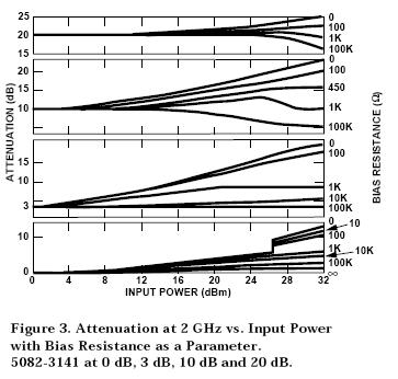
54 When the diode is forward biased, holes and electrons are injected into the I- region. This charge does not recombine instantaneously, but has a finite lifetime (t) in the I-region. If the PIN diode is reverse biased, there is no stored charge in the I-region and the device behaves like a Capacitance (CT) shunted by a parallel resistance (RP).
55 Forward Bias Condition: The PIN diode must be forward biased (Low Loss or ON State) so that the stored charge, Qs, is much larger than the RF induced charge that is added or removed from the I-region cyclically by the RF current. This relationship is shown by the inequality: Qs >> Irf / 2 pf.
56 Reverse Bias Condition: If large values of RF current are being switched, the reverse bias voltage must be large enough that the RF voltage during its forward excursion does not induce the flow of RF current through the PIN diode. If the PIN diode becomes warm when operating as a high power switch, the reverse bias voltage should be increased to minimize this effect.
57 PIN diodes are used to control RF power in circuits such as switches, attenuators, modulators and phase shifters. The process of controlling RF power naturally results in some of the RF power being dissipated in the controlling device.
58 As a PIN diode dissipates power, its junction temperature begins to rise. The diode's junction temperature depends on the amount of power dissipated, Pd, the ambient temperature Tamb, and the thermal impedance, ( qj), between the diode junction and the diode's ambient temperature.
59 The RF System Requirement that usually determines the choice of the particular PIN Diode to be used is the RF power that the switch must handle. The PIN Diode characteristically has relatively wide I-region and can therefore withstand larger RF Voltages than Varactors or microwave Schottky diodes.
60 An ideal PIN diode acts as a variable resistor controlled by dc current. In attenuation applications, the performance is independent of carrier power level or frequency.
61 Frequency Effect Attenuation as a function of power level at 2 GHz is shown for three types of diodes in Figures 1, 2, and 3. Corresponding data at 10 GHz is shown in Figures 4, 5, and 6. At the lower frequency, the longer period allows the charges to be influenced by the RF voltage.
62
63 Bias Current Effect A glance at Figure 3 will confirm that attenuation setting or bias level has a significant effect on high power behavior. The high power effects are most serious at intermediate bias current levels. At high bias currents, a large electric field is necessary in order to have a significant effect on the large number of charge carriers present in the intrinsic layer of the diode.
64
65 Load Resistance and Temperature Effects The temperature effects are related to the increases in the bias resistor value. Current, and therefore attenuation, rises with temperature with a voltage source, corresponding to the low values of bias resistance.
66 Treatment The simplest version of a PIN diode attenuator treatment is consists of one or more PIN diodes in shunt with a transmission line. This design provides a broadband reflective attenuator that can reach very high levels of attenuation, depending upon the number and electrical spacing of the diodes.
67 Shunt reflective attenuator
68 The performance of a real PIN diode, however, is limited by both carrier level and frequency because of rectification effects. The effects are more serious at low frequencies because the period is closer to the lifetime of the charge carriers in the diode intrinsic layer. General Microwave PIN diode attenuators cover the frequency range from 200 MHz to 40 GHz and are available in numerous configurations to permit the user to optimize system performance.
69 Applications It is used as a Photo Detector for most fiber optic application They are Used in electronic pre-amplifier to boost sensitivity They are Used as a variable resistor in at RF and microwave frequency
70 Widely used in RF modulator circuit to control RF intermodulation distortion In a phase shifter circuit considered as a lumped variable-impedance microwave circuit element. PIN diodes are utilized as series or shunt connected switches in phase shifter designs. The switched elements are either lengths of transmission line or reactive elements
71
72 When the forward bias control current of the PIN diode is varied continuously, it can be used for attenuating, leveling, and amplitude modulating an RF signal. When the control current is switched on and off, or in discrete steps, the device can be used for switching, pulse modulating, and phase shifting an RF signal
73 The microwave PIN diode's small physical size compared to a wavelength, high switching speed, and low package parasitic reactance, make it an ideal component for use in miniature, broadband RF signal control circuits
74 PIN diode has the ability to control large RF signal power while using much smaller levels of control power. In modulator circuit, PIN diode s minority carrier provide a low level of RF Intermodulation Distortion. (switching speed)
75 PIN DIODE ATTENUATOR CIRCUIT APPLICATIONS PIN diode attenuator circuits are used in automatic gain control (AGC) circuits and power leveling applications. The PIN diode attenuator may be a simple reflective attenuator, such as a series or shunt diode mounted across the transmission line. Some AGC attenuators are more complex networks that maintain impedance match to the input power and load as the attenuation is varied across its dynamic range.
76 Other methods are used to implement the AGC function, such as varying the gain of an RF transistor stage. The PIN diode AGC circuit results in lower frequency pulling and lower signal distortion.
77
Prepared by: Dr. Rishi Prakash, Dept of Electronics and Communication Engineering Page 1 of 5
 Microwave tunnel diode Some anomalous phenomena were observed in diode which do not follows the classical diode equation. This anomalous phenomena was explained by quantum tunnelling theory. The tunnelling
UNIT VIII-SPECIAL PURPOSE ELECTRONIC DEVICES. 1. Explain tunnel Diode operation with the help of energy band diagrams.
 UNIT III-SPECIAL PURPOSE ELECTRONIC DEICES 1. Explain tunnel Diode operation with the help of energy band diagrams. TUNNEL DIODE: A tunnel diode or Esaki diode is a type of semiconductor diode which is
1) A silicon diode measures a low value of resistance with the meter leads in both positions. The trouble, if any, is
 A silicon diode measures a low value of resistance with the meter leads in both positions. The trouble, if any, is") 1) A silicon diode measures a low value of resistance with the meter leads in both positions. The trouble, if any, is A [ ]) the diode is open. B [ ]) the diode is shorted to ground. C [v]) the diode is
1) A silicon diode measures a low value of resistance with the meter leads in both positions. The trouble, if any, is A [ ]) the diode is open. B [ ]) the diode is shorted to ground. C [v]) the diode is
1- Light Emitting Diode (LED)
") Content: - Special Purpose two terminal Devices: Light-Emitting Diodes, Varactor (Varicap)Diodes, Tunnel Diodes, Liquid-Crystal Displays. 1- Light Emitting Diode (LED) Light Emitting Diode is a photo electronic
Content: - Special Purpose two terminal Devices: Light-Emitting Diodes, Varactor (Varicap)Diodes, Tunnel Diodes, Liquid-Crystal Displays. 1- Light Emitting Diode (LED) Light Emitting Diode is a photo electronic
Objective Type Questions 1. Why pure semiconductors are insulators at 0 o K? 2. What is effect of temperature on barrier voltage? 3.
 Objective Type Questions 1. Why pure semiconductors are insulators at 0 o K? 2. What is effect of temperature on barrier voltage? 3. What is difference between electron and hole? 4. Why electrons have
ELECTRONIC DEVICES AND CIRCUITS
 ELECTRONIC DEVICES AND CIRCUITS 1. At room temperature the current in an intrinsic semiconductor is due to A. holes B. electrons C. ions D. holes and electrons 2. Work function is the maximum energy required
Electronic devices-i. Difference between conductors, insulators and semiconductors
 Electronic devices-i Semiconductor Devices is one of the important and easy units in class XII CBSE Physics syllabus. It is easy to understand and learn. Generally the questions asked are simple. The unit
CONTENTS. 2.2 Schrodinger's Wave Equation 31. PART I Semiconductor Material Properties. 2.3 Applications of Schrodinger's Wave Equation 34
 CONTENTS Preface x Prologue Semiconductors and the Integrated Circuit xvii PART I Semiconductor Material Properties CHAPTER 1 The Crystal Structure of Solids 1 1.0 Preview 1 1.1 Semiconductor Materials
Module 04.(B1) Electronic Fundamentals
 Electronic Fundamentals") 1.1a. Semiconductors - Diodes. Module 04.(B1) Electronic Fundamentals Question Number. 1. What gives the colour of an LED?. Option A. The active element. Option B. The plastic it is encased in. Option
1.1a. Semiconductors - Diodes. Module 04.(B1) Electronic Fundamentals Question Number. 1. What gives the colour of an LED?. Option A. The active element. Option B. The plastic it is encased in. Option
SRM INSTITUTE OF SCIENCE AND TECHNOLOGY (DEEMED UNIVERSITY)
") SRM INSTITUTE OF SCIENCE AND TECHNOLOGY (DEEMED UNIVERSITY) QUESTION BANK I YEAR B.Tech (II Semester) ELECTRONIC DEVICES (COMMON FOR EC102, EE104, IC108, BM106) UNIT-I PART-A 1. What are intrinsic and
SRM INSTITUTE OF SCIENCE AND TECHNOLOGY (DEEMED UNIVERSITY) QUESTION BANK I YEAR B.Tech (II Semester) ELECTRONIC DEVICES (COMMON FOR EC102, EE104, IC108, BM106) UNIT-I PART-A 1. What are intrinsic and
Downloaded from
 SOLID AND SEMICONDUCTOR DEVICES (EASY AND SCORING TOPIC) 1. Distinction of metals, semiconductor and insulator on the basis of Energy band of Solids. 2. Types of Semiconductor. 3. PN Junction formation
SYED AMMAL ENGINEERING COLLEGE
 SYED AMMAL ENGINEERING COLLEGE (Approved by the AICTE, New Delhi, Govt. of Tamilnadu and Affiliated to Anna University, Chennai) Established in 1998 - An ISO 9001:2008 Certified Institution Dr. E.M.Abdullah
Chapter 6. FM Circuits
 Chapter 6 FM Circuits Topics Covered 6-1: Frequency Modulators 6-2: Frequency Demodulators Objectives You should be able to: Explain the operation of an FM modulators and demodulators. Compare and contrast;
P-N Diodes & Applications
 P-N Diodes & Applications Outline Major junction diode applications are Electronics circuit control Rectifying (forward mode) Special break-down diodes: Zener and avalanche Switching Circuit tuning (varactor)
Lecture - 19 Microwave Solid State Diode Oscillator and Amplifier
 Basic Building Blocks of Microwave Engineering Prof. Amitabha Bhattacharya Department of Electronics and Communication Engineering Indian Institute of Technology, Kharagpur Lecture - 19 Microwave Solid
Review Energy Bands Carrier Density & Mobility Carrier Transport Generation and Recombination
 Review Energy Bands Carrier Density & Mobility Carrier Transport Generation and Recombination Current Transport: Diffusion, Thermionic Emission & Tunneling For Diffusion current, the depletion layer is
Optical Fiber Communication Lecture 11 Detectors
 Optical Fiber Communication Lecture 11 Detectors Warriors of the Net Detector Technologies MSM (Metal Semiconductor Metal) PIN Layer Structure Semiinsulating GaAs Contact InGaAsP p 5x10 18 Absorption InGaAs
Semiconductor Devices Lecture 5, pn-junction Diode
 Semiconductor Devices Lecture 5, pn-junction Diode Content Contact potential Space charge region, Electric Field, depletion depth Current-Voltage characteristic Depletion layer capacitance Diffusion capacitance
Chapter 1. Introduction
 Chapter 1 Introduction 1.1 Introduction of Device Technology Digital wireless communication system has become more and more popular in recent years due to its capability for both voice and data communication.
UNIT IX ELECTRONIC DEVICES
 UNT X ELECTRONC DECES Weightage Marks : 07 Semiconductors Semiconductors diode-- characteristics in forward and reverse bias, diode as rectifier. - characteristics of LED, Photodiodes, solarcell and Zener
Università degli Studi di Roma Tor Vergata Dipartimento di Ingegneria Elettronica. Analogue Electronics. Paolo Colantonio A.A.
 Università degli Studi di Roma Tor Vergata Dipartimento di Ingegneria Elettronica Analogue Electronics Paolo Colantonio A.A. 2015-16 Introduction: materials Conductors e.g. copper or aluminum have a cloud
Microwave Semiconductor Devices
 INDEX Avalanche breakdown, see reverse breakdown, Avalanche condition, 61 generalized, 62 Ballistic transport, 322, 435, 450 Bandgap, III-V-compounds, 387 Bandgap narrowing, Si, 420 BARITT device, 111,
EC6202- ELECTRONIC DEVICES AND CIRCUITS UNIT TEST-1 EXPECTED QUESTIONS
 EC6202- ELECTRONIC DEVICES AND CIRCUITS UNIT TEST-1 EXPECTED QUESTIONS 1. List the PN diode parameters. 1. Bulk Resistance. 2. Static Resistance/Junction Resistance (or) DC Forward Resistance 3. Dynamic
15 Transit Time and Tunnel NDR Devices
 15 Transit Time and Tunnel NDR Devices Schematics of Transit-time NDR diode. A packet of carriers (e.g., electrons) is generated in a confined and narrow zone (generation region) and injected into the
14.2 Photodiodes 411
 14.2 Photodiodes 411 Maximum reverse voltage is specified for Ge and Si photodiodes and photoconductive cells. Exceeding this voltage can cause the breakdown and severe deterioration of the sensor s performance.
Resonant Tunneling Device. Kalpesh Raval
 Resonant Tunneling Device Kalpesh Raval Outline Diode basics History of Tunnel diode RTD Characteristics & Operation Tunneling Requirements Various Heterostructures Fabrication Technique Challenges Application
SEMICONDUCTOR ELECTRONICS: MATERIALS, DEVICES AND SIMPLE CIRCUITS. Class XII : PHYSICS WORKSHEET
 SEMICONDUCT ELECTRONICS: MATERIALS, DEVICES AND SIMPLE CIRCUITS Class XII : PHYSICS WKSHEET 1. How is a n-p-n transistor represented symbolically? (1) 2. How does conductivity of a semiconductor change
Lecture 18: Photodetectors
 Lecture 18: Photodetectors Contents 1 Introduction 1 2 Photodetector principle 2 3 Photoconductor 4 4 Photodiodes 6 4.1 Heterojunction photodiode.................... 8 4.2 Metal-semiconductor photodiode................
Class Notes by. K.Elampari, Associate Professor of Physics, S.T.Hindu college, Nagercoil 1
 Class Notes by. K.Elampari, Associate Professor of Physics, S.T.Hindu college, Nagercoil 1 CHAPTER V- Micro Wave Devices Microwaves are a form of electromagnetic radiation with ranging from 1m to 1mm (or)
Chapter Semiconductor Electronics
 Chapter Semiconductor Electronics Q1. p-n junction is said to be forward biased, when [1988] (a) the positive pole of the battery is joined to the p- semiconductor and negative pole to the n- semiconductor
Semiconductor Devices
 Semiconductor Devices Modelling and Technology Source Electrons Gate Holes Drain Insulator Nandita DasGupta Amitava DasGupta SEMICONDUCTOR DEVICES Modelling and Technology NANDITA DASGUPTA Professor Department
Lecture 16 Microwave Detector and Switching Diodes
 Basic Building Blocks of Microwave Engineering Prof. Amitabha Bhattacharya Department of Electronics and Communication Engineering Indian Institute of Technology, Kharagpur Lecture 16 Microwave Detector
Photodiode: LECTURE-5
 LECTURE-5 Photodiode: Photodiode consists of an intrinsic semiconductor sandwiched between two heavily doped p-type and n-type semiconductors as shown in Fig. 3.2.2. Sufficient reverse voltage is applied
HOW DIODES WORK CONTENTS. Solder plated Part No. Lot No Cathode mark. Solder plated 0.
 www.joeknowselectronics.com Joe Knows, Inc. 1930 Village Center Circle #3-8830 Las Vegas, NV 89134 How Diodes Work Copyright 2013 Joe Knows Electronics HOW DIODES WORK Solder plated 0.4 1.6 There are several
Digital Integrated Circuits A Design Perspective. The Devices. Digital Integrated Circuits 2nd Devices
 Digital Integrated Circuits A Design Perspective The Devices The Diode The diodes are rarely explicitly used in modern integrated circuits However, a MOS transistor contains at least two reverse biased
DEPARTMENT OF ELECTRONICS AND COMMUNICATION ENGINEERING QUESTION BANK SUBJECT NAME & CODE: EC2403 & RF AND MICROWAVE ENGINEERING UNIT I
 FATIMA MICHAEL COLLEGE OF ENGINEERING & TECHNOLOGY Senkottai Village, Madurai Sivagangai Main Road, Madurai -625 020 An ISO 9001:2008 Certified Institution DEPARTMENT OF ELECTRONICS AND COMMUNICATION ENGINEERING
Section:A Very short answer question
 Section:A Very short answer question 1.What is the order of energy gap in a conductor, semi conductor, and insulator?. Conductor - no energy gap Semi Conductor - It is of the order of 1 ev. Insulator -
QUESTION BANK EC6201 ELECTRONIC DEVICES UNIT I SEMICONDUCTOR DIODE PART A. It has two types. 1. Intrinsic semiconductor 2. Extrinsic semiconductor.
 FATIMA MICHAEL COLLEGE OF ENGINEERING & TECHNOLOGY Senkottai Village, Madurai Sivagangai Main Road, Madurai - 625 020. [An ISO 9001:2008 Certified Institution] QUESTION BANK EC6201 ELECTRONIC DEVICES SEMESTER:
 Electronic Devices 1. Current flowing in each of the following circuits A and respectively are: (Circuit 1) (Circuit 2) 1) 1A, 2A 2) 2A, 1A 3) 4A, 2A 4) 2A, 4A 2. Among the following one statement is not
Zaid abdul zahra hassan. Dept.of physics-collage of education for pure sciences. Babylon university
 Tunnel diode: Zaid abdul zahra hassan Dept.of physics-collage of education for pure sciences Babylon university 1N3716 tunnel diode (with jumper for scale) A tunnel diode or Esaki diode is a type of semiconductor
Intrinsic Semiconductor
 Semiconductors Crystalline solid materials whose resistivities are values between those of conductors and insulators. Good electrical characteristics and feasible fabrication technology are some reasons
Electro - Principles I
 The PN Junction Diode Introduction to the PN Junction Diode Note: In this chapter we consider conventional current flow. Page 11-1 The schematic symbol for the pn junction diode the shown in Figure 1.
UNIT-III SOURCES AND DETECTORS. According to the shape of the band gap as a function of the momentum, semiconductors are classified as
 UNIT-III SOURCES AND DETECTORS DIRECT AND INDIRECT BAND GAP SEMICONDUCTORS: According to the shape of the band gap as a function of the momentum, semiconductors are classified as 1. Direct band gap semiconductors
MAHARASHTRA STATE BOARD OF TECHNICAL EDUCATION (Autonomous) (ISO/IEC Certified) Subject Code: Model Answer Page No: 1/
 (ISO/IEC Certified) Subject Code: Model Answer Page No: 1/") MAHARASHTRA STATE BOARD OF TECHNICAL EDUCATION (Autonomous) (ISO/IEC 27001 2005 Certified) SUMMER 13 EXAMINATION Subject Code: 12025 Model Answer Page No: 1/ Important Instructions to examiners: 1) The
MAHARASHTRA STATE BOARD OF TECHNICAL EDUCATION (Autonomous) (ISO/IEC 27001 2005 Certified) SUMMER 13 EXAMINATION Subject Code: 12025 Model Answer Page No: 1/ Important Instructions to examiners: 1) The
Fundamentals of Power Semiconductor Devices
 В. Jayant Baliga Fundamentals of Power Semiconductor Devices 4y Spri ringer Contents Preface vii Chapter 1 Introduction 1 1.1 Ideal and Typical Power Switching Waveforms 3 1.2 Ideal and Typical Power Device
Power Semiconductor Devices
 TRADEMARK OF INNOVATION Power Semiconductor Devices Introduction This technical article is dedicated to the review of the following power electronics devices which act as solid-state switches in the circuits.
Reg. No. : Question Paper Code : B.E./B.Tech. DEGREE EXAMINATION, NOVEMBER/DECEMBER Second Semester
 WK 5 Reg. No. : Question Paper Code : 27184 B.E./B.Tech. DEGREE EXAMINATION, NOVEMBER/DECEMBER 2015. Time : Three hours Second Semester Electronics and Communication Engineering EC 6201 ELECTRONIC DEVICES
Student Lecture by: Giangiacomo Groppi Joel Cassell Pierre Berthelot September 28 th 2004
 Student Lecture by: Giangiacomo Groppi Joel Cassell Pierre Berthelot September 28 th 2004 Lecture outline Historical introduction Semiconductor devices overview Bipolar Junction Transistor (BJT) Field
Optical Amplifiers. Continued. Photonic Network By Dr. M H Zaidi
 Optical Amplifiers Continued EDFA Multi Stage Designs 1st Active Stage Co-pumped 2nd Active Stage Counter-pumped Input Signal Er 3+ Doped Fiber Er 3+ Doped Fiber Output Signal Optical Isolator Optical
Lesson Plan. Week Theory Practical Lecture Day. Topic (including assignment / test) Day. Thevenin s theorem, Norton s theorem
 Day. Thevenin s theorem, Norton s theorem") Name of the faculty: GYANENDRA KUMAR YADAV Discipline: APPLIED SCIENCE(C.S.E,E.E.ECE) Year : 1st Subject: FEEE Lesson Plan Lesson Plan Duration: 31 weeks (from July, 2018 to April, 2019) Week Theory Practical
Name of the faculty: GYANENDRA KUMAR YADAV Discipline: APPLIED SCIENCE(C.S.E,E.E.ECE) Year : 1st Subject: FEEE Lesson Plan Lesson Plan Duration: 31 weeks (from July, 2018 to April, 2019) Week Theory Practical
Detectors for Optical Communications
 Optical Communications: Circuits, Systems and Devices Chapter 3: Optical Devices for Optical Communications lecturer: Dr. Ali Fotowat Ahmady Sep 2012 Sharif University of Technology 1 Photo All detectors
AN 1651 Analysis and design Of Analog Integrated Circuits. Two Mark Questions & Answers. Prepared By M.P.Flower queen Lecturer,EEE Dept.
 AN 1651 Analysis and design Of Analog Integrated Circuits Two Mark Questions & Answers Prepared By M.P.Flower queen Lecturer,EEE Dept. 1.write the poissons equation. UNIT I = charge density = electron
MAHARASHTRA STATE BOARD OF TECHNICAL EDUCATION (Autonomous) (ISO/IEC Certified) Summer 2016 EXAMINATIONS.
 (ISO/IEC Certified) Summer 2016 EXAMINATIONS.") Summer 2016 EXAMINATIONS Subject Code: 17321 Model Answer Important Instructions to examiners: 1) The answers should be examined by key words and not as word-to-word as given in the answer scheme. 2) The
Summer 2016 EXAMINATIONS Subject Code: 17321 Model Answer Important Instructions to examiners: 1) The answers should be examined by key words and not as word-to-word as given in the answer scheme. 2) The
Chapter 14 Semiconductor Electronics Materials Devices And Simple Circuits
 Class XII Chapter 14 Semiconductor Electronics Materials Devices And Simple Circuits Physics Question 14.1: In an n-type silicon, which of the following statement is true: (a) Electrons are majority carriers
Limiter Diodes Features Description Chip Dimensions Model DOT Diameter (Typ.) Chip Number St l Style Inches 4 11
 Chip Number St l Style Inches 4 11") Features Low Loss kw Coarse Limiters 200 Watt Midrange Limiters 10 mw Clean Up Limiters 210 20 Description Alpha has pioneered the microwave limiter diode. Because all phases of manufacturing, from design
Features Low Loss kw Coarse Limiters 200 Watt Midrange Limiters 10 mw Clean Up Limiters 210 20 Description Alpha has pioneered the microwave limiter diode. Because all phases of manufacturing, from design
ECE 340 Lecture 29 : LEDs and Lasers Class Outline:
 ECE 340 Lecture 29 : LEDs and Lasers Class Outline: Light Emitting Diodes Lasers Semiconductor Lasers Things you should know when you leave Key Questions What is an LED and how does it work? How does a
Key Questions. What is an LED and how does it work? How does a laser work? How does a semiconductor laser work? ECE 340 Lecture 29 : LEDs and Lasers
 Things you should know when you leave Key Questions ECE 340 Lecture 29 : LEDs and Class Outline: What is an LED and how does it How does a laser How does a semiconductor laser How do light emitting diodes
 Energy band diagrams Metals: 9. ELECTRONIC DEVICES GIST ρ= 10-2 to 10-8 Ω m Insulators: ρ> 10 8 Ω m Semiconductors ρ= 1 to 10 5 Ω m 109 A. Intrinsic semiconductors At T=0k it acts as insulator At room
CHAPTER 8 The PN Junction Diode
 CHAPTER 8 The PN Junction Diode Consider the process by which the potential barrier of a PN junction is lowered when a forward bias voltage is applied, so holes and electrons can flow across the junction
Electronic Circuits I. Instructor: Dr. Alaa Mahmoud
 Electronic Circuits I Instructor: Dr. Alaa Mahmoud alaa_y_emam@hotmail.com Chapter 27 Diode and diode application Outline: Semiconductor Materials The P-N Junction Diode Biasing P-N Junction Volt-Ampere
UNIT 3 Transistors JFET
 UNIT 3 Transistors JFET Mosfet Definition of BJT A bipolar junction transistor is a three terminal semiconductor device consisting of two p-n junctions which is able to amplify or magnify a signal. It
Vidyalankar F.Y. Diploma : Sem. II [CO/CD/CM/CW/IF] Basic Electronics V F V K. V K = 0.7 for Si = 0.3 for Ge
![Vidyalankar F.Y. Diploma : Sem. II [CO/CD/CM/CW/IF] Basic Electronics V F V K. V K = 0.7 for Si = 0.3 for Ge](/thumbs/94/121292009.jpg "Vidyalankar F.Y. Diploma : Sem. II [CO/CD/CM/CW/IF] Basic Electronics V F V K. V K = 0.7 for Si = 0.3 for Ge") F.Y. Diploma : Sem. II [CO/CD/CM/CW/IF] Basic Electronics Time : 3 Hrs. Prelim Question Paper Solution Marks : 100 Q.1 Attempt any TEN of the following: [20] Q.1(a) Draw characteristics of PN junction
F.Y. Diploma : Sem. II [CO/CD/CM/CW/IF] Basic Electronics Time : 3 Hrs. Prelim Question Paper Solution Marks : 100 Q.1 Attempt any TEN of the following: [20] Q.1(a) Draw characteristics of PN junction
SUMMER 13 EXAMINATION Subject Code: Model Answer Page No: / N
 Important Instructions to examiners: 1) The answers should be examined by key words and not as word-to-word as given in the model answer scheme. 2) The model answer and the answer written by candidate
EC6202-ELECTRONIC DEVICES AND CIRCUITS YEAR/SEM: II/III UNIT 1 TWO MARKS. 1. Define diffusion current.
 EC6202-ELECTRONIC DEVICES AND CIRCUITS YEAR/SEM: II/III UNIT 1 TWO MARKS 1. Define diffusion current. A movement of charge carriers due to the concentration gradient in a semiconductor is called process
COOPERATIVE PATENT CLASSIFICATION
 CPC H H03 COOPERATIVE PATENT CLASSIFICATION ELECTRICITY (NOTE omitted) BASIC ELECTRONIC CIRCUITRY H03B GENERATION OF OSCILLATIONS, DIRECTLY OR BY FREQUENCY-CHANGING, BY CIRCUITS EMPLOYING ACTIVE ELEMENTS
Lecture 11 - Microwave Semiconductors and Diodes
 Lecture 11 - Microwave Semiconductors and Diodes Microwave Active Circuit Analysis and Design Clive Poole and Izzat Darwazeh Academic Press Inc. Poole-Darwazeh 2015 Lecture 11 - Microwave Semiconductors
EDC Lecture Notes UNIT-1
 P-N Junction Diode EDC Lecture Notes Diode: A pure silicon crystal or germanium crystal is known as an intrinsic semiconductor. There are not enough free electrons and holes in an intrinsic semi-conductor
Power MOSFET Zheng Yang (ERF 3017,
 ECE442 Power Semiconductor Devices and Integrated Circuits Power MOSFET Zheng Yang (ERF 3017, email: yangzhen@uic.edu) Evolution of low-voltage (
 SEMICONDUCTOR EECTRONICS MATERIAS, DEVICES AND SIMPE CIRCUITS Important Points: 1. In semiconductors Valence band is almost filled and the conduction band is almost empty. The energy gap is very small
Electronics The basics of semiconductor physics
 Electronics The basics of semiconductor physics Prof. Márta Rencz, Gábor Takács BME DED 17/09/2015 1 / 37 The basic properties of semiconductors Range of conductivity [Source: http://www.britannica.com]
MICROWAVE ENGINEERING-II. Unit- I MICROWAVE MEASUREMENTS
 MICROWAVE ENGINEERING-II Unit- I MICROWAVE MEASUREMENTS 1. Explain microwave power measurement. 2. Why we can not use ordinary diode and transistor in microwave detection and microwave amplification? 3.
Key Questions ECE 340 Lecture 28 : Photodiodes
 Things you should know when you leave Key Questions ECE 340 Lecture 28 : Photodiodes Class Outline: How do the I-V characteristics change with illumination? How do solar cells operate? How do photodiodes
VALLIAMMAI ENGINEERING COLLEGE SRM Nagar, Kattankulathur
 VALLIAMMAI ENGINEERING COLLEGE SRM Nagar, Kattankulathur 603 203. DEPARTMENT OF ELECTRONICS & COMMUNICATION ENGINEERING SUBJECT QUESTION BANK : EC6201 ELECTRONIC DEVICES SEM / YEAR: II / I year B.E.ECE
Department of Electrical Engineering IIT Madras
 Department of Electrical Engineering IIT Madras Sample Questions on Semiconductor Devices EE3 applicants who are interested to pursue their research in microelectronics devices area (fabrication and/or
Optical Receivers Theory and Operation
 Optical Receivers Theory and Operation Photo Detectors Optical receivers convert optical signal (light) to electrical signal (current/voltage) Hence referred O/E Converter Photodetector is the fundamental
Semiconductor Detector Systems
 Semiconductor Detector Systems Helmuth Spieler Physics Division, Lawrence Berkeley National Laboratory OXFORD UNIVERSITY PRESS ix CONTENTS 1 Detector systems overview 1 1.1 Sensor 2 1.2 Preamplifier 3
Sharjah Indian School, Sharjah ELECTRONIC DEVICES - Class XII (Boys Wing) Page 01
 Page 01") ELECTRONIC DEVICES - Class XII (Boys Wing) Page 01 Electronics is the fast developing branch of Physics. Before the discovery of transistors in 1948, vacuum tubes (thermionic valves) were used as the building
ELECTRONIC DEVICES - Class XII (Boys Wing) Page 01 Electronics is the fast developing branch of Physics. Before the discovery of transistors in 1948, vacuum tubes (thermionic valves) were used as the building
Lecture Course. SS Module PY4P03. Dr. P. Stamenov
 Semiconductor Devices - 2013 Lecture Course Part of SS Module PY4P03 Dr. P. Stamenov School of Physics and CRANN, Trinity College, Dublin 2, Ireland Hilary Term, TCD 01 st of Feb 13 Diode Current Components
1 of 7 12/20/ :04 PM
 1 of 7 12/20/2007 11:04 PM Trusted Resource for the Working RF Engineer [ C o m p o n e n t s ] Build An E-pHEMT Low-Noise Amplifier Although often associated with power amplifiers, E-pHEMT devices are
Optodevice Data Book ODE I. Rev.9 Mar Opnext Japan, Inc.
 Optodevice Data Book ODE-408-001I Rev.9 Mar. 2003 Opnext Japan, Inc. Section 1 Operating Principles 1.1 Operating Principles of Laser Diodes (LDs) and Infrared Emitting Diodes (IREDs) 1.1.1 Emitting Principles
INTRODUCTION TO MOS TECHNOLOGY
 INTRODUCTION TO MOS TECHNOLOGY 1. The MOS transistor The most basic element in the design of a large scale integrated circuit is the transistor. For the processes we will discuss, the type of transistor
Lesson 08. Name and affiliation of the author: Professor L B D R P Wijesundera Department of Physics, University of Kelaniya.
 Lesson 08 Title of the Experiment: Identification of active components in electronic circuits and characteristics of a Diode, Zener diode and LED (Activity number of the GCE Advanced Level practical Guide
Diodes. Analog Electronics Lesson 4. Objectives and Overview:
 Analog Electronics Lesson 4 Diodes Objectives and Overview: This lesson will introduce p- and n-type material, how they form a junction that rectifies current, and familiarize you with basic p-n junction
PHYS 3050 Electronics I
 PHYS 3050 Electronics I Chapter 4. Semiconductor Diodes and Transistors Earth, Moon, Mars, and Beyond Dr. Jinjun Shan, Associate Professor of Space Engineering Department of Earth and Space Science and
15 - SEMICONDUCTOR ELECTRONICS: MATERIALS, DEVICES AND SIMPLE CIRCUITS Page 1
 15.1 Introduction MATERIALS, DEVICES AND SIMPLE CIRCUITS Page 1 The word electronics is coined from the words electron mechanics. The subject of electronics deals with the study of devices in which specific
This tutorial will suit all beginners who want to learn the fundamental concepts of transistors and transistor amplifier circuits.
 About the Tutorial An electronic signal contains some information which cannot be utilized if doesn t have proper strength. The process of increasing the signal strength is called as Amplification. Almost
Downloaded from
 Question 14.1: In an n-type silicon, which of the following statement is true: (a) Electrons are majority carriers and trivalent atoms are the dopants. (b) Electrons are minority carriers and pentavalent
Analog Electronic Circuits
 Analog Electronic Circuits Chapter 1: Semiconductor Diodes Objectives: To become familiar with the working principles of semiconductor diode To become familiar with the design and analysis of diode circuits
ANALYSIS AND DESIGN OF ANALOG INTEGRATED CIRCUITS
 ANALYSIS AND DESIGN OF ANALOG INTEGRATED CIRCUITS Fourth Edition PAUL R. GRAY University of California, Berkeley PAUL J. HURST University of California, Davis STEPHEN H. LEWIS University of California,
A Self-Biased Anti-parallel Planar Varactor Diode
 Page 356 A Self-Biased Anti-parallel Planar Varactor Diode Neal R. Erickson Department of Physics and Astronomy University of Massachusetts Amherst, MA 01003 Abstract A set of design criteria are presented
Class XII - Physics Semiconductor Electronics. Chapter-wise Problems
 lass X - Physics Semiconductor Electronics Materials, Device and Simple ircuit hapter-wise Problems Multiple hoice Question :- 14.1 The conductivity of a semiconductor increases with increase in temperature
Discuss the basic structure of atoms Discuss properties of insulators, conductors, and semiconductors
 Discuss the basic structure of atoms Discuss properties of insulators, conductors, and semiconductors Discuss covalent bonding Describe the properties of both p and n type materials Discuss both forward
HMPP-386x Series MiniPak Surface Mount RF PIN Diodes
 HMPP-86x Series MiniPak Surface Mount RF PIN Diodes Data Sheet Description/Applications These ultra-miniature products represent the blending of Avago Technologies proven semiconductor and the latest in
SETH JAI PARKASH POLYTECHNIC, DAMLA
 SETH JAI PARKASH POLYTECHNIC, DAMLA NAME OF FACULTY----------SANDEEP SHARMA DISCIPLINE---------------------- E.C.E (S.F) SEMESTER-------------------------2 ND SUBJECT----------------------------BASIC ELECTRONICS
AE53/AC53/AT53/AE103 ELECT. DEVICES & CIRCUITS DEC 2015
 Q.2 a. By using Norton s theorem, find the current in the load resistor R L for the circuit shown in Fig.1. (8) Fig.1 IETE 1 b. Explain Z parameters and also draw an equivalent circuit of the Z parameter
PHYSICS OF SEMICONDUCTOR DEVICES
 PHYSICS OF SEMICONDUCTOR DEVICES PHYSICS OF SEMICONDUCTOR DEVICES by J. P. Colinge Department of Electrical and Computer Engineering University of California, Davis C. A. Colinge Department of Electrical
FET Channel. - simplified representation of three terminal device called a field effect transistor (FET)
") FET Channel - simplified representation of three terminal device called a field effect transistor (FET) - overall horizontal shape - current levels off as voltage increases - two regions of operation 1.
FET Channel - simplified representation of three terminal device called a field effect transistor (FET) - overall horizontal shape - current levels off as voltage increases - two regions of operation 1.
Physics 160 Lecture 5. R. Johnson April 13, 2015
 Physics 160 Lecture 5 R. Johnson April 13, 2015 Half Wave Diode Rectifiers Full Wave April 13, 2015 Physics 160 2 Note that there is no ground connection on this side of the rectifier! Output Smoothing
Field Effect Transistors (npn)
") Field Effect Transistors (npn) gate drain source FET 3 terminal device channel e - current from source to drain controlled by the electric field generated by the gate base collector emitter BJT 3 terminal
Field Effect Transistors (npn) gate drain source FET 3 terminal device channel e - current from source to drain controlled by the electric field generated by the gate base collector emitter BJT 3 terminal
Section 2.3 Bipolar junction transistors - BJTs
 Section 2.3 Bipolar junction transistors - BJTs Single junction devices, such as p-n and Schottkty diodes can be used to obtain rectifying I-V characteristics, and to form electronic switching circuits