EOTPR Customer Case Studies. EUFANET Workshop: Findings OPEN?
|
|
|
- Berenice Clarke
- 5 years ago
- Views:
Transcription
1 EOTPR Customer Case Studies EUFANET Workshop: Findings OPEN?
2 OUTLINE o EOTPR introduction basic scheme o EOTPR OPEN customer case studies o Open on BGA trace (evaluation) o Open on embedded BGA trace o Open at C4 bump level


3 Why use THz for a TDR system? TDR EOTPR Qualitative technique Quantitative technique 3 3

4 Terahertz Engine Schematic core of all Terahertz products Ti:Sapphire fs laser Device under test THz Emitter Probe optical fibres THz Receiver optical delay Computer 4

5 Examples of failures identified by EOTPR in 2.5D packages: Shorts, Opens, and Resistive Opens. Proven detection capability up to die. Within RDL and TSV µ-bumps (top and bottom) C4 bumps (top and bottom) Substrate trace 5

6 EOTPR fault isolation in advanced packages Position of peaks provides fault location Interposer Substrate Si Die Opens or high impedances (resistive opens) are shown by EOTPR as positive peaks EOTPR intensity (a.u.) Shorted probe Bare substrate Interposer substrate Good unit -70 Shorts or low impedances are shown by EOTPR as negative peaks BGA Package Substrate Silicon Interposer Silicon Die 6
7 TeraView EOTPR: Customer case study I Open in package substrate Device A and B both have a FIB cut in an identical trace The position of the cut is separated by ~90 µm in the devices (measured from BGA to start of the FIB cut) EOTPR can clearly identify the difference in location of the open circuit in the two devices Device A FIB cuts in traces Device B 200 BGA feature Open circuit features Failed Device A Failed Device B µm Failed Device A Failed Device B 150 EOTPR signal (a.u.) EOTPR signal (a.u.) Distance into DUT (mm) Distance into DUT (mm)
 8 *Presented at IPFA 2012, paper")
8 TeraView EOTPR: Customer case study II Open in package substrate TDR EOTPR TDR result - Fault at substrate side EOTPR result - Distance-to-Defect accurately calculated and confirmed with PFA (see next slide) 8 *Presented at IPFA 2012, paper 19-68


9 TeraView EOTPR: Customer case study II Open in package substrate PFA result: Cu trace broken at Metal7 of the substrate Design layout - Actual Distance = µm PFA result confirms EOTPR fault loaction 9 *Presented at IPFA 2012, paper 19-68
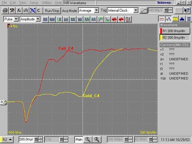
10 TeraView EOTPR customer case study III: Flip Chip An open fault was identified during electrical testing of a flip chip product. EOTPR was used to locate the fault within the failed unit. The plot below shows EOTPR waveforms from a reference bare substrate and the failed unit. The bare substrate terminates at the C4 bump pad, before the start of the C4. BGA Failed trace route C4 Contact feature Substrate termination Open in failed unit Bare substrate Failed unit


11 TeraView EOTPR customer case study III: Flip Chip The EOTPR waveforms show an open circuit in the failed unit, after the bare substrate termination. Substrate termination Open in failed unit From EOTPR we determine the fault is located 83 µm after the bare substrate termination, putting it at the die side of C4, likely at the UBM. The EOTPR fault location was subsequently confirmed by physical failure analysis as noncontact between UBM and Al contact pad. Physical failure analysis results: Good unit Failed unit C4 bump pad C4 bump 83 µm 80 µm C4 bump C4 bump pad UBM in contact with Al pad UBM not in contact with Al pad Bare substrate Failed unit
12 Comparison of EOTPR vs. conventional TDR Property EOTPR TDR EOTPR added value Input signal shape Impulse Step function EOTPR makes it easier to pinpoint faults as peak positions give fault locations. Frequency range DC to greater than 100 GHz DC to 35 GHz EOTPR higher frequency content allows for faster rise times compared to conventional TDR. Rise time < 10 ps (raw) < 6 ps (deconvolved) ~ 35 ps EOTPR faster rise time produces improved resolution compared to conventional TDR. Time base jitter < 30 femtoseconds ( seconds) > 500 femtoseconds ( seconds) EOTPR high time base stability allows for increase fault location accuracy compared to conventional TDR. Signal to noise > 64 db 45 db EOTPR high SNR increases its sensitivity to small changes in impedance
13 othanks you for your attention oquestions?
14 TeraView EOTPR: Accuracy We determine EOTPR System accuracy in the following way: Injected pulse reflects off device/interconnect Probe is displaced in 10µm steps along interconnect to demonstrate accuracy Change in position of reflected signal is measured Interconnects Probe Displacement Step size 10µm 14


15 TeraView EOTPR: Accuracy This demonstrates EOTPR has an accuracy of 30 femtoseconds. In a typical DUT this is equivalent to an accuracy of 10 µm. Reflection from end of test device track 10 repeat measurements collected at each step 0 µm 100 µm 10 µm steps 30 femtoseconds = 0.03 picoseconds = 10 µm 15


16 TeraView EOTPR: Customer case study III Package substrate impedance change EOTPR results III PFA results EOTPR signal (a.u.) I II Vendor 1 Cu trace Thinner trace Vendor 1 Vendor Distance in DUT /mm Vendor 2 Cu trace EOTPR result - show significant impedance differences between two substrate vendors. PFA result Cu trace width of vendor 1 thinner than vendor *Presented at IPFA 2012, paper 19-68
3D IC-Package-Board Co-analysis using 3D EM Simulation for Mobile Applications
 3D IC-Package-Board Co-analysis using 3D EM Simulation for Mobile Applications Darryl Kostka, CST of America Taigon Song and Sung Kyu Lim, Georgia Institute of Technology Outline Introduction TSV Array
Source: Nanju Na Jean Audet David R Stauffer IBM Systems and Technology Group
 Title: Package Model Proposal Source: Nanju Na (nananju@us.ibm.com) Jean Audet (jaudet@ca.ibm.com), David R Stauffer (dstauffe@us.ibm.com) Date: Dec 27 IBM Systems and Technology Group Abstract: New package
Fan-Out Solutions: Today, Tomorrow the Future Ron Huemoeller
 Fan-Out Solutions: Today, Tomorrow the Future Ron Huemoeller Corporate Vice President, WW RnD & Technology Strategy 1 In the Beginning ewlb 2 Fan Out Packaging Emerges Introduction of Fan Out (ewlb) Marketed
Packaging Fault Isolation Using Lock-in Thermography
 Packaging Fault Isolation Using Lock-in Thermography Edmund Wright 1, Tony DiBiase 2, Ted Lundquist 2, and Lawrence Wagner 3 1 Intersil Corporation; 2 DCG Systems, Inc.; 3 LWSN Consulting, Inc. Addressing
Signal Integrity Modeling and Measurement of TSV in 3D IC
 Signal Integrity Modeling and Measurement of TSV in 3D IC Joungho Kim KAIST joungho@ee.kaist.ac.kr 1 Contents 1) Introduction 2) 2.5D/3D Architectures with TSV and Interposer 3) Signal integrity, Channel
Christian Boit TUB Berlin University of Technology Sect. Semiconductor Devices. 1
 Semiconductor Device & Analysis Center Berlin University of Technology Christian Boit TUB Berlin University of Technology Sect. Semiconductor Devices Christian.Boit@TU-Berlin.DE 1 Semiconductor Device
Testing with Femtosecond Pulses
 Testing with Femtosecond Pulses White Paper PN 200-0200-00 Revision 1.3 January 2009 Calmar Laser, Inc www.calmarlaser.com Overview Calmar s femtosecond laser sources are passively mode-locked fiber lasers.
Electronic Package Failure Analysis Using TDR
 Application Note Electronic Package Failure Analysis Using TDR Introduction Time Domain Reflectometry (TDR) measurement methodology is increasing in importance as a nondestructive method for fault location
Microprobe-enabled Terahertz sensing applications
 Microprobe-enabled Terahertz sensing applications World of Photonics, Laser 2015, Munich Protemics GmbH Aachen, Germany Terahertz microprobing technology: Taking advantage of Terahertz range benefits without
Signal Integrity Design of TSV-Based 3D IC
 Signal Integrity Design of TSV-Based 3D IC October 24, 21 Joungho Kim at KAIST joungho@ee.kaist.ac.kr http://tera.kaist.ac.kr 1 Contents 1) Driving Forces of TSV based 3D IC 2) Signal Integrity Issues
Signal Integrity Modeling and Simulation for IC/Package Co-Design
 Signal Integrity Modeling and Simulation for IC/Package Co-Design Ching-Chao Huang Optimal Corp. October 24, 2004 Why IC and package co-design? The same IC in different packages may not work Package is
Foundry WLSI Technology for Power Management System Integration
 1 Foundry WLSI Technology for Power Management System Integration Chuei-Tang Wang, Chih-Lin Chen, Jeng-Shien Hsieh, Victor C.Y. Chang, Douglas Yu R&D,TSMC Oct. 2016 2 Motivation Outline PMIC system integration
Microprobe-enabled Terahertz sensing applications
 Microprobe-enabled Terahertz sensing applications M. Nagel Protemics GmbH, Aachen, Germany TERAHERTZ LOW FREQUENCY MICROWAVES IR UV X-RAY RADIO WAVES VISIBLE GAMMA RAY THz frequency range 0.1 THz 1 THz
Capabilities of Flip Chip Defects Inspection Method by Using Laser Techniques
 Capabilities of Flip Chip Defects Inspection Method by Using Laser Techniques Sheng Liu and I. Charles Ume* School of Mechanical Engineering Georgia Institute of Technology Atlanta, Georgia 3332 (44) 894-7411(P)
True Three-Dimensional Interconnections
 True Three-Dimensional Interconnections Satoshi Yamamoto, 1 Hiroyuki Wakioka, 1 Osamu Nukaga, 1 Takanao Suzuki, 2 and Tatsuo Suemasu 1 As one of the next-generation through-hole interconnection (THI) technologies,
Considerations in High-Speed High Performance Die-Package-Board Co-Design. Jenny Jiang Altera Packaging Department October 2014
 Considerations in High-Speed High Performance Die-Package-Board Co-Design Jenny Jiang Altera Packaging Department October 2014 Why Co-Design? Complex Multi-Layer BGA Package Horizontal and vertical design
Modeling, Design, and Demonstration of 2.5D Glass Interposers for 16-Channel 28 Gbps Signaling Applications
 Modeling, Design, and Demonstration of 2.5D Glass Interposers for 16-Channel 28 Gbps Signaling Applications Brett Sawyer, Bruce C. Chou, Saumya Gandhi, Jack Mateosky, Venky Sundaram, and Rao Tummala 3D
The 3D Silicon Leader
 The 3D Silicon Leader 3D Silicon IPD for smaller and more reliable Implantable Medical Devices ATW on Advanced Packaging for Wireless Medical Devices Mohamed Mehdi Jatlaoui, Sébastien Leruez, Olivier Gaborieau,
Picosecond Laser Stimulation status, applications & challenges
 Picosecond Laser Stimulation status, applications & challenges Vincent POUGET IMS, University of Bordeaux, Talence, France Laboratoire de l Intégration, du Matériau au Système CNRS UMR 5218 Outline Picosecond
Testing with 40 GHz Laser Sources
 Testing with 40 GHz Laser Sources White Paper PN 200-0500-00 Revision 1.1 January 2009 Calmar Laser, Inc www.calmarlaser.com Overview Calmar s 40 GHz fiber lasers are actively mode-locked fiber lasers.
Fraunhofer IZM - ASSID
 FRAUNHOFER-INSTITUT FÜR Zuverlässigkeit und Mikrointegration IZM Fraunhofer IZM - ASSID All Silicon System Integration Dresden Heterogeneous 3D Wafer Level System Integration 3D system integration is one
Acoustic microscopy for 3D-SiP failure analysis
 Acoustic microscopy for 3D-SiP failure analysis Peter Czurratis PVA TePla Analytical Systems GmbH, Westhausen, Germany Sebastian Brand Fraunhofer Center for Applied Microstructure Diagnostics (CAM) Halle,
2.5D Platform (Examples of products produced to date are shown here to demonstrate Amkor's production capabilities)
") Wafer Finishing & Flip Chip Stacking interconnects have emerged to serve a wide range of 2.5D- & 3D- packaging applications and architectures that demand very high performance and functionality at the
Wafer Finishing & Flip Chip Stacking interconnects have emerged to serve a wide range of 2.5D- & 3D- packaging applications and architectures that demand very high performance and functionality at the
VITESSE SEMICONDUCTOR CORPORATION. Bandwidth (MHz) VSC
 VSC") Features optimized for high speed optical communications applications Integrated AGC Fibre Channel and Gigabit Ethernet Low Input Noise Current Differential Output Single 5V Supply with On-chip biasing
Features optimized for high speed optical communications applications Integrated AGC Fibre Channel and Gigabit Ethernet Low Input Noise Current Differential Output Single 5V Supply with On-chip biasing
PLL Synchronizer User s Manual / Version 1.0.6
 PLL Synchronizer User s Manual / Version 1.0.6 AccTec B.V. Den Dolech 2 5612 AZ Eindhoven The Netherlands phone +31 (0) 40-2474321 / 4048 e-mail AccTecBV@tue.nl Contents 1 Introduction... 3 2 Technical
Analysis of 60 GHz flip-chipped package using EM toolbased time-domain reflectometry
 Analysis of 6 GHz flip-chipped package using EM toolbased time-domain reflectometry Citation for published version (APA): Kazim, M. I., & Herben, M. H. A. J. (212). Analysis of 6 GHz flip-chipped package
New Wave SiP solution for Power
 New Wave SiP solution for Power Vincent Lin Corporate R&D ASE Group APEC March 7 th, 2018 in San Antonio, Texas. 0 Outline Challenges Facing Human Society Energy, Environment and Traffic Autonomous Driving
SHELLCASE-TYPE WAFER-LEVEL PACKAGING SOLUTIONS: RF CHARACTERIZATION AND MODELING
 SHELLCASE-TYPE WAFER-LEVEL PACKAGING SOLUTIONS: RF CHARACTERIZATION AND MODELING M Bartek 1, S M Sinaga 1, G Zilber 2, D Teomin 2, A Polyakov 1, J N Burghartz 1 1 Delft University of Technology, Lab of
Silicon Interposers enable high performance capacitors
 Interposers between ICs and package substrates that contain thin film capacitors have been used previously in order to improve circuit performance. However, with the interconnect inductance due to wire
Broadband Beamforming of Terahertz Pulses with a Single-Chip 4 2 Array in Silicon
 Forum for Electromagnetic Research Methods and Application Technologies (FERMAT) Broadband Beamforming of Terahertz Pulses with a Single-Chip 4 2 Array in Silicon M. Mahdi Assefzadeh and Aydin Babakhani
Innovative ultra-broadband ubiquitous Wireless communications through terahertz transceivers ibrow
 Project Overview Innovative ultra-broadband ubiquitous Wireless communications through terahertz transceivers ibrow Mar-2017 Presentation outline Project key facts Motivation Project objectives Project
Enabling Parallel Testing at Sort for High Power Products
 Enabling Parallel Testing at Sort for High Power Products Abdel Abdelrahman Tim Swettlen 2200 Mission College Blvd. M/S SC2-07 Santa Clara, CA 94536 Abdel.Abdelrahman@intel.com Tim.Swettlen@intel.com Agenda
Picosecond Pulses for Test & Measurement
 Picosecond Pulses for Test & Measurement White Paper PN 200-0100-00 Revision 1.1 September 2003 Calmar Optcom, Inc www.calamropt.com Overview Calmar s picosecond laser sources are actively mode-locked
Enabling concepts: Packaging Technologies
 Enabling concepts: Packaging Technologies Ana Collado / Liam Murphy ESA / TEC-EDC 01/10/2018 ESA UNCLASSIFIED - For Official Use Enabling concepts: Packaging Technologies Drivers for the future: Higher
2.5D & 3D Package Signal Integrity A Paradigm Shift
 2.5D & 3D Package Signal Integrity A Paradigm Shift Nozad Karim Technology & Platform Development November, 2011 Enabling a Microelectronic World Content Traditional package signal integrity vs. 2.5D/3D
z t h l g 2009 John Wiley & Sons, Inc. Published 2009 by John Wiley & Sons, Inc.
 x w z t h l g Figure 10.1 Photoconductive switch in microstrip transmission-line geometry: (a) top view; (b) side view. Adapted from [579]. Copyright 1983, IEEE. I g G t C g V g V i V r t x u V t Z 0 Z
Design and experimental realization of the chirped microstrip line
 Chapter 4 Design and experimental realization of the chirped microstrip line 4.1. Introduction In chapter 2 it has been shown that by using a microstrip line, uniform insertion losses A 0 (ω) and linear
MICROELECTRONICS ASSSEMBLY TECHNOLOGIES. The QFN Platform as a Chip Packaging Foundation
 West Coast Luncheon January 15, 2014. PROMEX PROMEX INDUSTRIES INC. MICROELECTRONICS ASSSEMBLY TECHNOLOGIES The QFN Platform as a Chip Packaging Foundation 3075 Oakmead Village Drive Santa Clara CA Ɩ 95051
High Speed Digital Systems Require Advanced Probing Techniques for Logic Analyzer Debug
 JEDEX 2003 Memory Futures (Track 2) High Speed Digital Systems Require Advanced Probing Techniques for Logic Analyzer Debug Brock J. LaMeres Agilent Technologies Abstract Digital systems are turning out
Electrical Test Vehicle for High Density Fan-Out WLP for Mobile Application. Institute of Microelectronics 22 April 2014
 Electrical Test Vehicle for High Density Fan-Out WLP for Mobile Application Institute of Microelectronics 22 April 2014 Challenges for HD Fan-Out Electrical Design 15-20 mm 7 mm 6 mm SI/PI with multilayer
Integrated Photonics using the POET Optical InterposerTM Platform
 Integrated Photonics using the POET Optical InterposerTM Platform Dr. Suresh Venkatesan CIOE Conference Shenzhen, China Sept. 5, 2018 POET Technologies Inc. TSXV: PUBLIC POET PTK.V Technologies Inc. PUBLIC
3D Si Interposer Design and Electrical Performance Study
 DesignCon 2013 3D Si Interposer Design and Electrical Performance Study Mandy (Ying) Ji, Rambus Inc. Ming Li, Rambus Inc. Julia Cline, Rambus Inc. Dave Secker, Rambus Inc. Kevin Cai, Rambus Inc. John Lau,
Design and Modeling of Through-Silicon Vias for 3D Integration
 Design and Modeling of Through-Silicon Vias for 3D Integration Ivan Ndip, Brian Curran, Gerhard Fotheringham, Jurgen Wolf, Stephan Guttowski, Herbert Reichl Fraunhofer IZM & BeCAP @ TU Berlin IEEE Workshop
450mm and Moore s Law Advanced Packaging Challenges and the Impact of 3D
 450mm and Moore s Law Advanced Packaging Challenges and the Impact of 3D Doug Anberg VP, Technical Marketing Ultratech SOKUDO Lithography Breakfast Forum July 10, 2013 Agenda Next Generation Technology
Optimal design methodology for RF SiP - from project inception to volume manufacturing
 Optimal design methodology for RF SiP - from project inception to volume manufacturing Chris Barratt Insight SiP 905 rue Albert Einstein Valbonne France 06560 Outline RF SiP Technologies Design Methodology
Parallel vs. Serial Inter-plane communication using TSVs
 Parallel vs. Serial Inter-plane communication using TSVs Somayyeh Rahimian Omam, Yusuf Leblebici and Giovanni De Micheli EPFL Lausanne, Switzerland Abstract 3-D integration is a promising prospect for
450mm patterning out of darkness Backend Process Exposure Tool SOKUDO Lithography Breakfast Forum July 10, 2013 Doug Shelton Canon USA Inc.
 450mm patterning out of darkness Backend Process Exposure Tool SOKUDO Lithography Breakfast Forum 2013 July 10, 2013 Doug Shelton Canon USA Inc. Introduction Half Pitch [nm] 2013 2014 2015 2016 2017 2018
Si-Interposer Collaboration in IC/PKG/SI. Eric Chen
 Si-Interposer Collaboration in IC/PKG/SI Eric Chen 4/Jul/2014 Design Overview U-bump Logic IC Mem IC C4 bump Logic IC Silicon/Organic substrate Interposer Mem IC CAP Package substrate Solder Ball VRM BGA
A 3.9 ns 8.9 mw 4 4 Silicon Photonic Switch Hybrid-Integrated with CMOS Driver
 A 3.9 ns 8.9 mw 4 4 Silicon Photonic Switch Hybrid-Integrated with CMOS Driver A. Rylyakov, C. Schow, B. Lee, W. Green, J. Van Campenhout, M. Yang, F. Doany, S. Assefa, C. Jahnes, J. Kash, Y. Vlasov IBM
High Frequency Electrical Model of Through Wafer Via for 3-D Stacked Chip Packaging
 High Frequency Electrical Model of Through Wafer Via for 3-D Stacked Chip Packaging Chunghyun Ryu, Jiwang Lee, Hyein Lee, *Kwangyong Lee, *Taesung Oh, and Joungho Kim Terahertz Interconnection and Package
Flip-Chip for MM-Wave and Broadband Packaging
 1 Flip-Chip for MM-Wave and Broadband Packaging Wolfgang Heinrich Ferdinand-Braun-Institut für Höchstfrequenztechnik (FBH) Berlin / Germany with contributions by F. J. Schmückle Motivation Growing markets
Designing for Femtosecond Pulses
 Designing for Femtosecond Pulses White Paper PN 200-1100-00 Revision 1.1 July 2013 Calmar Laser, Inc www.calmarlaser.com Overview Calmar s femtosecond laser sources are passively mode-locked fiber lasers.
Development of a 20 GS/s Sampling Chip in 130nm CMOS Technology
 Development of a 20 GS/s Sampling Chip in 130nm CMOS Technology 2009 IEEE Nuclear Science Symposium, Orlando, Florida, October 28 th 2009 Jean-Francois Genat On behalf of Mircea Bogdan 1, Henry J. Frisch
Diverse Lasers Support Key Microelectronic Packaging Tasks
 Diverse Lasers Support Key Microelectronic Packaging Tasks Written by D Muller, R Patzel, G Oulundsen, H Halou, E Rea 23 July 2018 To support more sophisticated and compact tablets, phones, watches and
Application Note. Signal Integrity Modeling. SCSI Connector and Cable Modeling from TDR Measurements
 Application Note SCSI Connector and Cable Modeling from TDR Measurements Signal Integrity Modeling SCSI Connector and Cable Modeling from TDR Measurements Dima Smolyansky TDA Systems, Inc. http://www.tdasystems.com
Preparing for the Future: Upgrades of the CMS Pixel Detector
 : KSETA Plenary Workshop, Durbach, KIT Die Forschungsuniversität in der Helmholtz-Gemeinschaft www.kit.edu Large Hadron Collider at CERN Since 2015: proton proton collisions @ 13 TeV Four experiments:
AIR-COUPLED PHOTOCONDUCTIVE ANTENNAS
 AIR-COUPLED PHOTOCONDUCTIVE ANTENNAS Report: Air-Coupled Photoconductive Antennas In this paper, we present air-coupled terahertz photoconductive antenna (THz-PCAs) transmitters and receivers made on high-resistive
A Technical Discussion of TDR Techniques, S-parameters, RF Sockets, and Probing Techniques for High Speed Serial Data Designs
 A Technical Discussion of TDR Techniques, S-parameters, RF Sockets, and Probing Techniques for High Speed Serial Data Designs Presenter: Brian Shumaker DVT Solutions, LLC, 650-793-7083 b.shumaker@comcast.net
IEEE CX4 Quantitative Analysis of Return-Loss
 IEEE CX4 Quantitative Analysis of Return-Loss Aaron Buchwald & Howard Baumer Mar 003 Return Loss Issues for IEEE 0G-Base-CX4 Realizable Is the spec realizable with standard packages and I/O structures
The Design of E-band MMIC Amplifiers
 The Design of E-band MMIC Amplifiers Liam Devlin, Stuart Glynn, Graham Pearson, Andy Dearn * Plextek Ltd, London Road, Great Chesterford, Essex, CB10 1NY, UK; (lmd@plextek.co.uk) Abstract The worldwide
Laminate Based Fan-Out Embedded Die Technologies: The Other Option
 Laminate Based Fan-Out Embedded Die Technologies: The Other Option Theodore (Ted) G. Tessier, Tanja Karila*, Tuomas Waris*, Mark Dhaenens and David Clark FlipChip International, LLC 3701 E University Drive
Chip Assembly on MID (Molded Interconnect Device) A Path to Chip Modules with increased Functionality
 A Path to Chip Modules with increased Functionality") T e c h n o l o g y Dr. Werner Hunziker Chip Assembly on MID (Molded Interconnect Device) A Path to Chip Modules with increased Functionality The MID (Molded Interconnect Device) technology enables the
T e c h n o l o g y Dr. Werner Hunziker Chip Assembly on MID (Molded Interconnect Device) A Path to Chip Modules with increased Functionality The MID (Molded Interconnect Device) technology enables the
Si photonics for the Zettabyte Era. Marco Romagnoli. CNIT & TeCIP - Scuola Superiore Sant Anna
 Si photonics for the Zettabyte Era Marco Romagnoli CNIT & TeCIP - Scuola Superiore Sant Anna Semicon 2013 Dresden 8-10 October 2013 Zetabyte era Disaggregation at system level Integration at chip level
Optical Bus for Intra and Inter-chip Optical Interconnects
 Optical Bus for Intra and Inter-chip Optical Interconnects Xiaolong Wang Omega Optics Inc., Austin, TX Ray T. Chen University of Texas at Austin, Austin, TX Outline Perspective of Optical Backplane Bus
AC-2 Calibration Substrate
 AC-2 Calibration Substrate AC-2 calibration substrate is designed to provide accurate probe tip calibration of MPI TITAN RF probe family with ground-signal-ground (GSG) probe tips configuration and accommodates
EMERGING SUBSTRATE TECHNOLOGIES FOR PACKAGING
 EMERGING SUBSTRATE TECHNOLOGIES FOR PACKAGING Henry H. Utsunomiya Interconnection Technologies, Inc. Suwa City, Nagano Prefecture, Japan henryutsunomiya@mac.com ABSTRACT This presentation will outline
A high resolution bunch arrival time monitor system for FLASH / XFEL
 A high resolution bunch arrival time monitor system for FLASH / XFEL K. Hacker, F. Löhl, F. Ludwig, K.H. Matthiesen, H. Schlarb, B. Schmidt, A. Winter October 24 th Principle of the arrival time detection
TODAY S electronic systems are becoming more complex
 Nondestructive Analysis of Interconnection in Two-Die BGA Using TDR Ming-Kun Chen, Cheng-Chi Tai, Member, IEEE, and Yu-Jung Huang, Senior Member, IEEE Abstract Nondestructive analysis (NDA) is one of the
Probe Card Characterization in Time and Frequency Domain
 Gert Hohenwarter GateWave Northern, Inc. Probe Card Characterization in Time and Frequency Domain Company Logo 2007 San Diego, CA USA Objectives Illuminate differences between Time Domain (TD) and Frequency
Non-Linear Transmission Line Comb Generator
 Page 1 The is a GaAs Schottky diode based non-linear transmission line comb generator. It is optimized for at input frequencies of 1 16 GHz and minimum input drive powers of +16 dbm. Harmonic content is
3D TSV Micro Cu Column Chip-to-Substrate/Chip Assmbly/Packaging Technology
 3D TSV Micro Cu Column Chip-to-Substrate/Chip Assmbly/Packaging Technology by Seung Wook Yoon, *K. T. Kang, W. K. Choi, * H. T. Lee, Andy C. B. Yong and Pandi C. Marimuthu STATS ChipPAC LTD, 5 Yishun Street
5G: THE NEXT DISRUPTIVE TECHNOLOGY IN PRODUCTION TEST
 5G: THE NEXT DISRUPTIVE TECHNOLOGY IN PRODUCTION TEST Daniel Bock, Ph.D. Mike Bishop Jeff Damm Michael Engelhardt Michael Hemena Robert Murphy Balbir Singh Introduction The development of 5G / WiGig products
Si Photonics Technology Platform for High Speed Optical Interconnect. Peter De Dobbelaere 9/17/2012
 Si Photonics Technology Platform for High Speed Optical Interconnect Peter De Dobbelaere 9/17/2012 ECOC 2012 - Luxtera Proprietary www.luxtera.com Overview Luxtera: Introduction Silicon Photonics: Introduction
2.C A Substrate-Independent Noncontact Electro-Optic Probe Using Total Internal Reflection. 5. LLE Review 27, (1986).
.") LLE REVIEW, Volume 32 transmission lines and the DUT may be fabricated on a common substrate, eliminating the need for wirebond connections. 3. Photoconductive switching and electro-optic sampling allow
LLE REVIEW, Volume 32 transmission lines and the DUT may be fabricated on a common substrate, eliminating the need for wirebond connections. 3. Photoconductive switching and electro-optic sampling allow
Agilent Technologies High-Definition Multimedia
 Agilent Technologies High-Definition Multimedia Interface (HDMI) Cable Assembly Compliance Test Test Solution Overview Using the Agilent E5071C ENA Option TDR Last Update 013/08/1 (TH) Purpose This slide
EVALUATION OF THE NEAR-FIELD INJECTION METHOD AT INTEGRATED CIRCUIT LEVEL
 1 EVALUATION OF THE NEAR-FIELD INJECTION METHOD AT INTEGRATED CIRCUIT LEVEL A. Boyer 1,2, B. Vrignon 3, J. Shepherd 3, M. Cavarroc 1,2 1 CNRS, LAAS, 7 avenue du colonel Roche, F-31400 Toulouse, France
Silicon Photonics Transceivers for Hyper Scale Datacenters: Deployment and Roadmap
 Silicon Photonics Transceivers for Hyper Scale Datacenters: Deployment and Roadmap Peter De Dobbelaere Luxtera Inc. 09/19/2016 Luxtera Proprietary www.luxtera.com Luxtera Company Introduction $100B+ Shift
Advances in X-Ray Technology for Semicon Applications Keith Bryant and Thorsten Rother
 Advances in X-Ray Technology for Semicon Applications Keith Bryant and Thorsten Rother X-Ray Champions, Telspec, Yxlon International Agenda The x-ray tube, the heart of the system Advances in digital detectors
Mass transfer with elastomer stamps for microled displays.
 Frontiers in Assembly Mass transfer with elastomer stamps for microled displays. Matt Meitl X-Celeprint, Inc. mmeitl@x-celeprint.com 1 The best materials for the best displays The materials identify the
Limiter Diodes Features Description Chip Dimensions Model DOT Diameter (Typ.) Chip Number St l Style Inches 4 11
 Chip Number St l Style Inches 4 11") Features Low Loss kw Coarse Limiters 200 Watt Midrange Limiters 10 mw Clean Up Limiters 210 20 Description Alpha has pioneered the microwave limiter diode. Because all phases of manufacturing, from design
Features Low Loss kw Coarse Limiters 200 Watt Midrange Limiters 10 mw Clean Up Limiters 210 20 Description Alpha has pioneered the microwave limiter diode. Because all phases of manufacturing, from design
Hot Topics and Cool Ideas in Scaled CMOS Analog Design
 Engineering Insights 2006 Hot Topics and Cool Ideas in Scaled CMOS Analog Design C. Patrick Yue ECE, UCSB October 27, 2006 Slide 1 Our Research Focus High-speed analog and RF circuits Device modeling,
TIGER Femtosecond and Picosecond Ti:Sapphire Lasers. Customized systems with SESAM technology*
 TIGER Femtosecond and Picosecond Ti:Sapphire Lasers Customized systems with SESAM technology* www.lumentum.com Data Sheet The TIGER femtosecond and picosecond lasers combine soliton mode-locking, a balance
Cost-minimized Double Die DRAM Packaging for Ultra-High Performance DDR3 and DDR4 Multi-Rank Server DIMMs
 Cost-minimized Double Die DRAM Packaging for Ultra-High Performance DDR3 and DDR4 Multi-Rank Server DIMMs Richard Crisp 1, Bill Gervasi 2, Wael Zohni 1, Bel Haba 3 1 Invensas Corp, 2902 Orchard Parkway,
Min Tao, Ph. D, Ashok Prabhu, Akash Agrawal, Ilyas Mohammed, Ph. D, Bel Haba, Ph. D Oct , IWLPC
 PACKAGE-ON-PACKAGE INTERCONNECT FOR FAN-OUT WAFER LEVEL PACKAGES Min Tao, Ph. D, Ashok Prabhu, Akash Agrawal, Ilyas Mohammed, Ph. D, Bel Haba, Ph. D Oct 18-20 2016, IWLPC 1 Outline Laminate to Fan-Out
Semiconductor and LED Markets. Jon Sabol Vice President and General Manager Semiconductor and LED Division
 Semiconductor and LED Markets Jon Sabol Vice President and General Manager Semiconductor and LED Division Semiconductor & LED Investing in Semiconductor and LED $ Millions 300 200 27% CAGR 100 0 * FY06
MP 4.3 Monolithic CMOS Distributed Amplifier and Oscillator
 MP 4.3 Monolithic CMOS Distributed Amplifier and Oscillator Bendik Kleveland, Carlos H. Diaz 1 *, Dieter Vook 1, Liam Madden 2, Thomas H. Lee, S. Simon Wong Stanford University, Stanford, CA 1 Hewlett-Packard
Measurement Results for a High Throughput MCM
 Measurement Results for a High Throughput MCM Funding: Paul Franzon Toby Schaffer, Alan Glaser, Steve Lipa North Carolina State University paulf@ncsu.edu www.ece.ncsu.edu/erl Outline > Heterogeneous System
Characterization of Alternate Power Distribution Methods for 3D Integration
 Characterization of Alternate Power Distribution Methods for 3D Integration David C. Zhang, Madhavan Swaminathan, David Keezer and Satyanarayana Telikepalli School of Electrical and Computer Engineering,
Investigate the characteristics of PIN Photodiodes and understand the usage of the Lightwave Analyzer component.
 PIN Photodiode 1 OBJECTIVE Investigate the characteristics of PIN Photodiodes and understand the usage of the Lightwave Analyzer component. 2 PRE-LAB In a similar way photons can be generated in a semiconductor,
Femtosecond Laser Simulation Facility for SEE IC Testing
 Femtosecond Laser Simulation Facility for SEE IC Testing Andrey N. Egorov, Alexander I. Chumakov, Oleg B. Mavritskiy, Alexander A. Pechenkin, Dmitry V. Savchenkov, Vitaliy A. Telets, Andrey V. Yanenko
ARCHIVE Automated Topside and Bottomside Testing of POP Packages on a Robotic Handler Eric Pensa, Willie Jerrels Texas Instruments
 ARCHIVE 2008 KEY CHALLENGES AND TECHNOLOGY TRENDS IN SOCKET DESIGN Automated Topside and Bottomside Testing of POP Packages on a Robotic Handler Eric Pensa, Willie Jerrels Texas Instruments High Speed
Nan Ya Plastics Corp.
 Nan Ya Plastics Corp. The Signal Integrity Study with Fiber Weave Effect Speaker: Peter Liang Electro Material Div. Copper Clad Laminate Unit Nanya CCL 1 Outline: -Demand of High Data Rate For Transmission
Extending Acoustic Microscopy for Comprehensive Failure Analysis Applications
 Extending Acoustic Microscopy for Comprehensive Failure Analysis Applications Sebastian Brand, Matthias Petzold Fraunhofer Institute for Mechanics of Materials Halle, Germany Peter Czurratis, Peter Hoffrogge
Modeling of the SiGe power HBT IM Distortion
 Modeling of the SiGe power HBT IM Distortion P.Sakalas %,$, M.Schröter %, L.Kornau &, W.Kraus & % Dresden University of Technology, Mommsenstrasse 13, 01062 Dresden, Germany & Atmel Germany GmbH, Theresienstrasse
Quality Assurance for the ATLAS Pixel Sensor
 Quality Assurance for the ATLAS Pixel Sensor 1st Workshop on Quality Assurance Issues in Silicon Detectors J. M. Klaiber-Lodewigs (Univ. Dortmund) for the ATLAS pixel collaboration Contents: - role of
A Solution of Test, Inspection and Evaluation for Blind Signal Waveform on a Board
 A Solution of Test, Inspection and Evaluation for Blind Signal Waveform on a Board Tatsumi Watabe, Makoto Kawamura, & Hiroyuki Yamakoshi S.E.R. Corporation Conference Ready mm/dd/2014 2016 BiTS Workshop
Flexible Hybrid Electronics Fabricated with High-Performance COTS ICs using RTI CircuitFilm TM Technology
 Flexible Hybrid Electronics Fabricated with High-Performance COTS ICs using RTI CircuitFilm TM Technology Scott Goodwin 1, Erik Vick 2 and Dorota Temple 2 1 Micross Advanced Interconnect Technology Micross
Effect of Aging on Power Integrity of Digital Integrated Circuits
 Effect of Aging on Power Integrity of Digital Integrated Circuits A. Boyer, S. Ben Dhia Alexandre.boyer@laas.fr Sonia.bendhia@laas.fr 1 May 14 th, 2013 Introduction and context Long time operation Harsh
Optical Interconnection and Clocking for Electronic Chips
 1 Optical Interconnection and Clocking for Electronic Chips Aparna Bhatnagar and David A. B. Miller Department of Electrical Engineering Stanford University, Stanford CA 9430 ABSTRACT As the speed of electronic
Design Considerations for Highly Integrated 3D SiP for Mobile Applications
 Design Considerations for Highly Integrated 3D SiP for Mobile Applications FDIP, CA October 26, 2008 Joungho Kim at KAIST joungho@ee.kaist.ac.kr http://tera.kaist.ac.kr Contents I. Market and future direction