Cost-minimized Double Die DRAM Packaging for Ultra-High Performance DDR3 and DDR4 Multi-Rank Server DIMMs
|
|
|
- Rudolf Foster
- 6 years ago
- Views:
Transcription
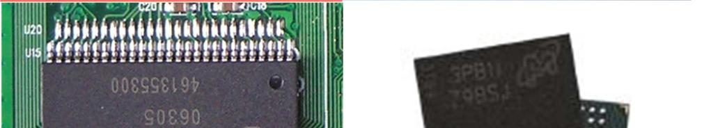
1 Cost-minimized Double Die DRAM Packaging for Ultra-High Performance DDR3 and DDR4 Multi-Rank Server DIMMs Richard Crisp 1, Bill Gervasi 2, Wael Zohni 1, Bel Haba 3 1 Invensas Corp, 2902 Orchard Parkway, San Jose, CA USA 2 Discobolus Designs, 22 Foliate Way, Ladera Ranch, CA USA 3 Tessera Inc, 3025 Orchard Parkway, San Jose, CA USA 1 rcrisp@invensas.com Abstract A cost-minimized generation-spanning double die DRAM packaging (DDP) technology suitable for making ultra-high performance high-capacity server DIMMs for both the DDR3 and DDR4 DRAM generations was developed. Using existing wirebond-based manufacturing infrastructure it is immediately deployable with no new assembly equipment required. Significant results were obtained relating to performance enhancement and cost reduction versus existing packaging and DIMM designs. Both die are mounted face down in the package with each showing identical performance. Bin split yields are enhanced significantly. The package ballout features placement of the command and address terminals in the center of the package permitting single-layer routing of the timing-critical address and command bus at the DIMM level. Data and Data Strobe signals have shorter routing stubs on the DIMM. The improved PCB layout resulting from the new ballout resulted in a quadrank RDIMM capable of operating at over 1600MT/s in a two DIMM per channel configuration: 50% faster than standard DIMMs. The face-down laterally displaced die arrangement with a sub-1mm package thickness reduces the thermal impedance by 25% versus conventional DDPs. Total assembly cost is the lowest of any DDP and on a per-die basis is lower than Single Die Packaging. Keywords DDR3, DDR4, RDIMM, LRDIMM, Hypercloud, DDP, wirebond, RDL 1. Introduction The design approach used was to identify clockrate limiting features of standard DRAM package and DIMM designs and to correct them using co-design of the DRAM package/ballout and DIMM while looking for opportunities for cost reduction. Focus areas for performance scaling were stub minimization for the DQ / DQ Strobe nets and command-address (C/A) bus, layer count reduction in the DIMM raw card and improved thermal performance. Conventional double die DRAM packages (DDPs) are designed to be footprint-compatible with single die packages (SDPs). All feature die stacked atop each other 1-xxxx-xxxx-4/10/$ IEEE without lateral displacement. Electrical connections are accomplished using wirebonds. The simplest type features back to back die with the lower die mounted face-down and the upper die mounted face up (Fig 1a). Data bus signals from the two die are wire-or connected. The upper die has long wirebonds that connect to the centrally-located bond pads and extend half way across the die to be bonded to the underlying substrate. The lower die wirebonds are made through a window in the substrate like conventional single die packages. The structure therefore has asymmetric signal and power delivery connections to the two die that causes the upper die s electrical performance to be degraded. Another approach uses a redistribution layer (RDL) on each die to move the bonding pads from the middle spine to the periphery region and mounts both die face up with the two die separated by a spacer die so that the wirebonds from the lower die are not crushed by the upper die (Fig 1b). The RDL process adds significant cost, approximately $300 per 300mm wafer, and the added RDL structure increases the capacitance of the signals routed across the die, degrading the performance. For both approaches, because the two die are stacked vertically without lateral displacement, some of the heat from the lower die must pass through the upper die, increasing its operating temperature. Furthermore both schemes feature topside wire loops that must be protected by overmolding. That increases the thickness of the package, further degrading the thermal performance versus single die packages. 2. Package Structure The double die package developed in this work overcomes each of the shortcomings of the previous DDPs described above. Figure 2 shows the new structure. Each die is mounted face down and is wirebonded through its own window. We have called this structure Dual Face Down (DFD ). Electrically both die perform near-identically as shown in the shmoo plot of Figure 3. The data was measured on a production VLSI tester from a sample of 15 randomly chosen units operated at 95C. The DFD has no top-facing wire loops so it needs less topside encapsulation resulting in a thinner structure of less than 1mm. Combined with the lateral displacement of the two die, the thermal impedance is reduced by 25% 13th Int l Symposium on Quality Electronic Design
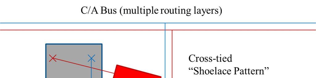
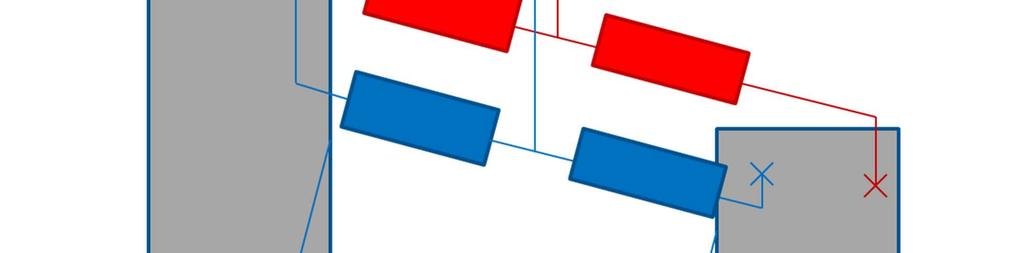
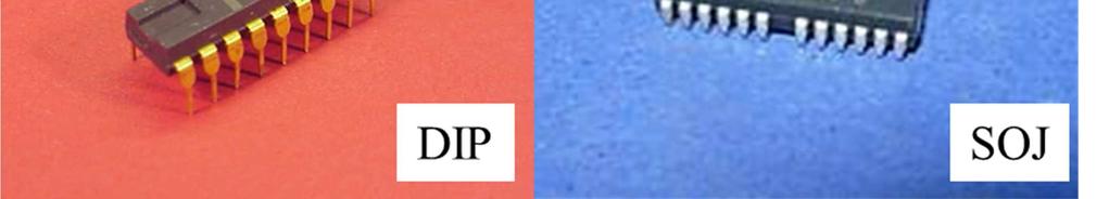
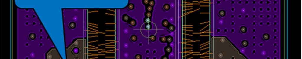
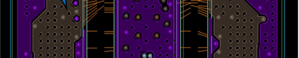
2 versus conventional DDPs. (Figure 4). The thinner package also reduces airflow resistance between DIMMs installed in systems further improving the cooling efficiency. Because both die have nearly identical electrical performance matching that of an SDP DRAM, bin split yields are significantly improved over standard DDPs. Figure 5 shows production sort results for a controlled experiment wherein 1000 units of the DFD were compared with 1000 control units. The control units were designed to mimic the top die of the opposing face DDP of figure 1a. Die for the experiment came from the same wafer lot. Since the control did not include substrate routing to connect to the lower die nor did it include the lower die, the sort results for the control are somewhat optimistic. Yet each die in the DFD showed a 67% improvement of sort yield to the highest speed bin versus the control. Equally important, no difference was observed in top versus bottom die sort yield indicating truly symmetric performance of the two die; monolithic performance in a double die package was achieved. The DFD has a simple and short process flow through the manufacturing line. It is the only DDP that can be made using single pass wirebonding. Manufacturing the DFD therefore costs less than either of the two DDP alternatives of Figure 1. A detailed assembly cost model revealed that the packaging cost per die assembled using the DFD structure was lower than either of the DDPs and is actually less than the SDP due to fewer process steps required for packaging a given number of die (Table 1). The cost of gold bond wire dominates the cost of the opposing face DDP of Figure 1a, while RDL cost dominates the dual face up DDP of Figure 1b. For example, assuming $300 RDL cost and 1200 good die per wafer, the RDL cost alone is $0.25/die, which is 25% more than the entire packaging cost of a SDP DRAM according to the cost model. An added benefit of the fact that the DFD represents the lowest cost method for packaging a given number of DRAM die is that DIMMs can be made using single sided assembly without compromising capacity, further reducing manufacturing cost for a given capacity DIMM: they are not limited to quadrank usage only. 3. Ballout Considerations The ballout for the DFD was developed in conjunction with the design of a quadrank DDR3 RDIMM. The critical nets that were optimized were the data / data strobe nets and the C/A bus. Double sided assembly used for RDIMMs requires that like-named C/A bus signals for pairs of packages placed in discrete sites on opposite sides of the DIMM from one another are electrically interconnected forming localized breakout regions. A global C/A bus routes through each breakout region to connect each site to the common C/A bus (Figure 6). Connections from the breakouts to the common C/A bus create stubs that can be up to 7mm long (Figure 7). At low frequency operation the stubs have little effect on the signal integrity, but as frequencies increase, signal reflections degrade the signal quality and timing margin and can cause functional failure. This creates a serious obstacle for operation beyond 1600MT/s. Mass-market DRAMs have always had signal terminals arranged into two groups that are laterally displaced on opposite sides of the centerline of the DRAM die with a gap between them. The first DRAMs were packaged in Dual Inline Packages (DIP). The DIP was replaced by the SOJ followed by the TSOP. In each case the signal terminals were disposed in single columns placed on opposite edges of the DRAM package. When the chipscale BGA was introduced, the single column of terminals evolved into two groups of three columns of terminals separated by a window through which wirebonds that interconnect the DRAM pads to the package substrate are placed. In all cases there was a gap between these two groups of signal terminals placed on opposite sides of the centerline of the DRAM die (Fig 8). This is the primary factor determining the length of the stubs on the C/A bus in the breakout region. Only recently has the length of the stubs become a limiting factor for DIMM frequency scaling. Exploiting the fact that the DFD has two laterallydisplaced bonding windows (Fig 2) on the substrate it is practical to place the C/A bus signals in the center of the package in adjacent columns (Fig 9). This greatly simplifies the cross-tie routing in the breakout region leading to a significant reduction in C/A bus stub length to 2mm for each signal in the breakout (Fig 10). A simulation comparing the C/A signals on DIMMs constructed using conventional DRAM packaging versus the DFD is shown in Fig 11. The simulation shows a 16% improvement in voltage margin at 75% higher operating frequency for the DFD. The signals for the DFD also show significantly less ringing versus the conventional ballout. The simplified breakout routing allows the outer surface of the DIMM PCB to have a higher percentage covered with a solid copper flood, leading to improved heat spreading and a more effective power plane with reduced signal impedance discontinuities arising from breaks in the reference plane. The signal ordering for the DFD s C/A terminals was set so that it mates without signal crossings to the register on the RDIMM used to buffer the C/A bus. This signal assignment scheme allows wider signal spacing reducing crosstalk. The combination of these advantages allows the C/A bus to be routed on a single layer (Fig 12)
3 versus the two layers required when a conventional ballout is used. Using a single layer for routing timing-critical C/A bus signals avoids differential propagation velocity and impedance variation of the signals when carried on separate layers, both of which degrade timing margin. Note that this timing skew cannot be compensated by the memory controller unlike data bus skew. As operating frequency is increased, this advantage will become of greater significance. The DQ and DQ Strobe nets are timing-critical and are sensitive to stub lengths. In order to minimize the length of the stubs that interconnect the various DQ and DQ Strobe signals together, the terminals were placed adjacent to the top edge of the package as shown in the ballout of Fig 9. By orienting the DFD packages that are placed on the same side of the DIMM PCB in a configuration so that the DQ/DQ Strobes from a pair of such packages are facing each other, the length of the stub interconnecting the signals is minimized as shown in Fig 12. This reduces the stub length to 4.5mm compared to a conventional BGA ballout at 6.5mm. 4. Substrate Design Using a four layer substrate in the DFD package allowed the DQ nets inside the DFD package to be referenced to the Vss plane with the Address and Clock nets referenced to the Vdd plane (Fig 13) as specified in the JEDEC DIMM standards for the DIMM PCB. This further improves the signal integrity by implementing a consistent set of design rules for signal return current paths for the entire system signal path from memory controller through DRAM package to the DRAM. 5. Applicability to LRDIMM and Hypercloud DIMMs The LRDIMM differs from the RDIMM in that the DQ and DQ Strobe signals are buffered[1]. The data buffer is placed in the central region of the LRDIMM. This requires all data and data strobes to be routed from each DRAM package to the buffer and then routed back to the edge connector which demands additional routing layers versus an RDIMM. Since the LRDIMM is plugged into an edge connector, the thickness of the DIMM PCB is fixed. Adding PCB layers necessarily requires a reduction of the thickness of the dielectric layers separating the power planes and routing layers. Unless the width of the traces is made narrower, the characteristic impedance of the etched traces is decreased and can lead to signal reflections arising from impedance discontinuities that diminish voltage and timing margin. Trace width is limited by the precision of the control of the etching process, with such narrower traces being more costly to manufacture within tolerance. Because the DFD s C/A bus routes on a single layer and other interconnections lay out cleanly, the layer count is reduced leading to nominal impedances being attainable with normal dimensional control keeping raw card costs from rising. The Hypercloud architecture is similar to the LRDIMM in that the DQ and DQ Strobe signals are buffered, but unlike the LRDIMM the buffering is provided by a number of data buffer devices placed between the edge connector and the DRAM package array on the DIMM PCB[2]. The 11.5 x 11.5 mm package outline of the DFD supports placement of the buffers without requiring growth of the vertical height of the DIMM. In fact a simple modification of the RDIMM PCB will enable the Hypercloud data buffers to be mounted on the PCB making conversion of an RDIMM design to Hypercloud a straightforward matter. 6. Measured Results A quadrank RDIMM was produced using 72 one gigabit die placed into 36 DFD packages (Fig 14). Unlike RDIMMs based on JEDEC-approved raw cards which are limited to 800 to 1066MT/s operation when used with two DIMMs per channel (2DPC), the DFD-based RDIMM was demonstrated to operate over 1600MT/s using die that when offered in SDPs, are sold up to 1866MT/s. An eye diagram measured by probing the DQ and DQ Strobe signals of an RDIMM using DFDs in a 2DPCconfigured system operating at 1600MT/s is shown in Fig 15. Probes were soldered to the signals on the DRAM side of the series damping resistors and measurements were made using a 12GHz bandwidth Digital Signal Analyzer (DSA). To validate the symmetry of the performance of the two die contained within a single DFD package, probes were soldered to the DQ and DQ Strobes of the two die contained within the same package. The DQ and DQ Strobe signal waveform transitions and voltage levels are nearly identical (Fig 16). 7. Applicability to Future DRAM Generations The DDR4 generation of DRAM is targeted to reach system operational speed up to 3200MT/s, approximately twice the speed of the highest official DDR3 system speed today[3]. Reaching these speeds will require great care being given to signal integrity and PCB layout. Stub lengths, differential propagation velocity induced skew and noise on signal reference planes will need to be minimized. The DFD s characteristics offer advantages in solving all of these challenges. The numerous improvements offered by the DFD are directly usable for dual die DDR4 packages with all the same advantages offered to the DDR3 DRAM generation providing a generation-spanning multi-die packaging technology. As data transfer rates scale to 3200MT/s and beyond the many advantages of the DFD and its ballout scheme will become of greater importance and may


![com/article/519386- Basics_of_LRDIMM.php [2] http:// www.netlist.](/docs-images/78/77012575/images/4-7.jpg "com/products/ppt/hc_gibabyte_brief_1. 0.pdf [3] http://ddr4.")
4 represent the only feasible way to reach these system frequencies. In particular the central location of the C/A terminals combined with single-layer routability may therefore prove to be an important innovation in DRAM packaging and become the preferred ballout scheme for future generations of DRAM or other high speed memory technologies that may replace DRAM. The DFD overcomes the performance disadvantages of previous DDP packaging for DRAMs. These important performance advantages combined with the fact that the DFD is the lowest cost method for packaging a given quantity of DRAM may completely change the landscape of how memory die are packaged in performance demanding applications. Table 1: Cost Summary. Package Total Type Assembly & Package Cost Per Die Assembly & Package Cost DFD $0.34 $0.17 DDR-RDL $0.83 $ DDP- Opposing Face $0.42 $0.21 SDP $0.20 $ References [1] Basics_of_LRDIMM.php [2] pdf [3] Figure 2: Dual face down package (DFD) Figure 3: Shmoo plot from VLSI 95C, 15 unit sample size Figure 4: Thermal Impedance vs Airflow Figure 1: Conventional DDP packages


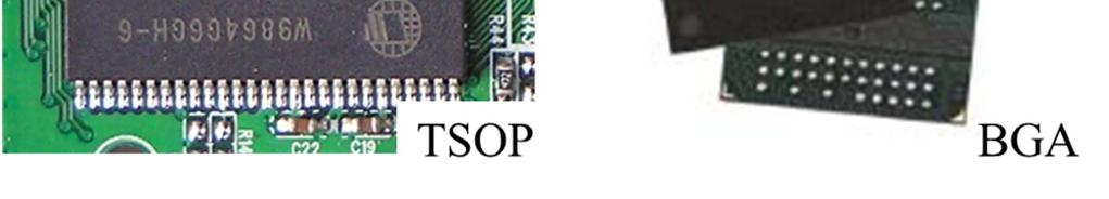


5 Figure 8: DRAM historical package evolution Figure 5: Production speed binning results Figure 6: Double sided assembly electrical connections Figure 13: DFD substrate layout showing reference planes Figure 7: C/A bus stubs in breakout region
6 Figure 9: DFD ball assignment Figure 10: RDIMM breakout region detail: DFD (left), Conventional JEDEC (right) Figure 14: Quadrank DDR3 RDIMM using DFD packages
7 Figure 11: C/A bus simulation: DFD RDIMM vs conventional raw card Figure 12: single layer C/A Bus routing through breakout regions
8 Figure 15: Read cycle eye 1600MT/s Figure 16: Read Cycle showing symmetric performance of both die in same package
Relationship Between Signal Integrity and EMC
 Relationship Between Signal Integrity and EMC Presented by Hasnain Syed Solectron USA, Inc. RTP, North Carolina Email: HasnainSyed@solectron.com 06/05/2007 Hasnain Syed 1 What is Signal Integrity (SI)?
Microcircuit Electrical Issues
 Microcircuit Electrical Issues Distortion The frequency at which transmitted power has dropped to 50 percent of the injected power is called the "3 db" point and is used to define the bandwidth of the
Min Tao, Ph. D, Ashok Prabhu, Akash Agrawal, Ilyas Mohammed, Ph. D, Bel Haba, Ph. D Oct , IWLPC
 PACKAGE-ON-PACKAGE INTERCONNECT FOR FAN-OUT WAFER LEVEL PACKAGES Min Tao, Ph. D, Ashok Prabhu, Akash Agrawal, Ilyas Mohammed, Ph. D, Bel Haba, Ph. D Oct 18-20 2016, IWLPC 1 Outline Laminate to Fan-Out
The number of layers The number and types of planes (power and/or ground) The ordering or sequence of the layers The spacing between the layers
 The ordering or sequence of the layers The spacing between the layers") PCB Layer Stackup PCB layer stackup (the ordering of the layers and the layer spacing) is an important factor in determining the EMC performance of a product. The following four factors are important with
PCB Layer Stackup PCB layer stackup (the ordering of the layers and the layer spacing) is an important factor in determining the EMC performance of a product. The following four factors are important with
High Speed Digital Systems Require Advanced Probing Techniques for Logic Analyzer Debug
 JEDEX 2003 Memory Futures (Track 2) High Speed Digital Systems Require Advanced Probing Techniques for Logic Analyzer Debug Brock J. LaMeres Agilent Technologies Abstract Digital systems are turning out
SINCE the performance of personal computers (PCs) has
 has") 334 IEEE TRANSACTIONS ON CIRCUITS AND SYSTEMS II: EXPRESS BRIEFS, VOL. 57, NO. 5, MAY 2010 Multi-Slot Main Memory System for Post DDR3 Jaejun Lee, Sungho Lee, and Sangwook Nam, Member, IEEE Abstract This
334 IEEE TRANSACTIONS ON CIRCUITS AND SYSTEMS II: EXPRESS BRIEFS, VOL. 57, NO. 5, MAY 2010 Multi-Slot Main Memory System for Post DDR3 Jaejun Lee, Sungho Lee, and Sangwook Nam, Member, IEEE Abstract This
Overcoming Obstacles to Closing Timing for DDR and Beyond. John Ellis Sr. Staff R&D Engineer Synopsys, Inc.
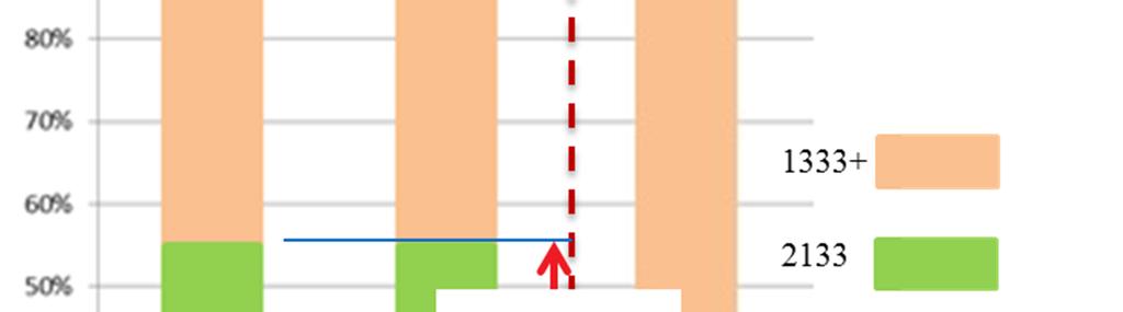
 Overcoming Obstacles to Closing Timing for DDR3-1600 and Beyond John Ellis Sr. Staff R&D Engineer Synopsys, Inc. Agenda Timing budgets 1600 2133Mbps? Static vs. Dynamic Uncertainty Sources Benefits of
PCB Trace Impedance: Impact of Localized PCB Copper Density
 PCB Trace Impedance: Impact of Localized PCB Copper Density Gary A. Brist, Jeff Krieger, Dan Willis Intel Corp Hillsboro, OR Abstract Trace impedances are specified and controlled on PCBs as their nominal
PI3DPX1207B Layout Guideline. Table of Contents. 1 Layout Design Guideline Power and GROUND High-speed Signal Routing...
 PI3DPX1207B Layout Guideline Table of Contents 1 Layout Design Guideline... 2 1.1 Power and GROUND... 2 1.2 High-speed Signal Routing... 3 2 PI3DPX1207B EVB layout... 8 3 Related Reference... 8 Page 1
DDR4 memory interface: Solving PCB design challenges
 DDR4 memory interface: Solving PCB design challenges Chang Fei Yee - July 23, 2014 Introduction DDR SDRAM technology has reached its 4th generation. The DDR4 SDRAM interface achieves a maximum data rate
Signal Technologies 1
 Signal Technologies 1 Gunning Transceiver Logic (GTL) - evolution Evolved from BTL, the backplane transceiver logic, which in turn evolved from ECL (emitter-coupled logic) Setup of an open collector bus
How to anticipate Signal Integrity Issues: Improve my Channel Simulation by using Electromagnetic based model
 How to anticipate Signal Integrity Issues: Improve my Channel Simulation by using Electromagnetic based model HSD Strategic Intent Provide the industry s premier HSD EDA software. Integration of premier
Overcoming the Challenges of HDI Design
 ALTIUMLIVE 2018: Overcoming the Challenges of HDI Design Susy Webb Design Science Sr PCB Designer San Diego Oct, 2018 1 Challenges HDI Challenges Building the uvia structures The cost of HDI (types) boards
Intel 82566/82562V Layout Checklist (version 1.0)
") Intel 82566/82562V Layout Checklist (version 1.0) Project Name Fab Revision Date Designer Intel Contact SECTION CHECK ITEMS REMARKS DONE General Ethernet Controller Obtain the most recent product documentation
Intel 82566/82562V Layout Checklist (version 1.0) Project Name Fab Revision Date Designer Intel Contact SECTION CHECK ITEMS REMARKS DONE General Ethernet Controller Obtain the most recent product documentation
Silicon Interposers enable high performance capacitors
 Interposers between ICs and package substrates that contain thin film capacitors have been used previously in order to improve circuit performance. However, with the interconnect inductance due to wire
Sherlock Solder Models
 Introduction: Sherlock Solder Models Solder fatigue calculations in Sherlock are accomplished using one of the many solder models available. The different solder models address the type of package that
Successful SATA 6 Gb/s Equipment Design and Development By Chris Cicchetti, Finisar 5/14/2009
 Successful SATA 6 Gb/s Equipment Design and Development By Chris Cicchetti, Finisar 5/14/2009 Abstract: The new SATA Revision 3.0 enables 6 Gb/s link speeds between storage units, disk drives, optical
A Two-Layer Board Intellectual Property to Reduce Electromagnetic Radiation
 A Two-Layer Board Intellectual Property to Reduce Electromagnetic Radiation Nansen Chen 1, Hongchin Lin 2 1 Digital TV BU, MediaTek Inc. No.1, Dusing Rd.1, Hsinchu Science Park, Hsinchu 300, Taiwan nansen.chen@mediatek.com
Chapter 2. Literature Review
 Chapter 2 Literature Review 2.1 Development of Electronic Packaging Electronic Packaging is to assemble an integrated circuit device with specific function and to connect with other electronic devices.
Effective Routing of Multiple Loads
 feature column BEYOND DESIGN Effective Routing of Multiple Loads by Barry Olney In a previous Beyond Design, Impedance Matching: Terminations, I discussed various termination strategies and concluded that
TMS320C6474 DDR2 Implementation Guidelines
 TMS320C6474 Implementation Guidelines Ronald Lerner... ABSTRACT This document provides implementation instructions for the interface contained on the C6474 DSP. Contents 1 Prerequisites... 2 2 C6474 Supported
Manufacture and Performance of a Z-interconnect HDI Circuit Card Abstract Introduction
 Manufacture and Performance of a Z-interconnect HDI Circuit Card Michael Rowlands, Rabindra Das, John Lauffer, Voya Markovich EI (Endicott Interconnect Technologies) 1093 Clark Street, Endicott, NY 13760
Low Jitter, Low Emission Timing Solutions For High Speed Digital Systems. A Design Methodology
 Low Jitter, Low Emission Timing Solutions For High Speed Digital Systems A Design Methodology The Challenges of High Speed Digital Clock Design In high speed applications, the faster the signal moves through
8. QDR II SRAM Board Design Guidelines
 8. QDR II SRAM Board Design Guidelines November 2012 EMI_DG_007-4.2 EMI_DG_007-4.2 This chapter provides guidelines for you to improve your system's signal integrity and layout guidelines to help successfully
PDS Impact for DDR Low Cost Design
 PDS Impact for DDR3-1600 Low Cost Design Jack W.C. Lin Sr. AE Manager jackl@cadence.com Aug. g 13 2013 Cadence, OrCAD, Allegro, Sigrity and the Cadence logo are trademarks of Cadence Design Systems, Inc.
MICTOR. High-Speed Stacking Connector
 MICTOR High-Speed Stacking Connector Electrical Performance Report for the 0.260" (6.6-mm) Stack Height Connector.......... Connector With Typical Footprint................... Connector in a System Report
Signal/Power Integrity Analysis of High-Speed Memory Module with Meshed Reference Plane 1
 , pp.119-128 http//dx.doi.org/10.14257/ijca.2018.11.7.10 Signal/Power Integrity Analysis of High-Speed Memory Module with Meshed Reference Plane 1 Moonjung Kim Institute of IT Convergence Technology, Dept.
Modeling System Signal Integrity Uncertainty Considerations
 white paper Intel FPGA Modeling System Signal Integrity Uncertainty Considerations Authors Ravindra Gali High-Speed I/O Applications Engineering, Intel Corporation Zhi Wong High-Speed I/O Applications
Digital Power Module Enables Fast Load Transient POL with Simple Cooling Design
 White Paper Digital Power Module Enables Fast Load Transient POL with Simple Cooling Design Introduction The ever-increasing demands of FPGAs, processors and ASICs are pushing point-of-load (POL) power
Laminate Based Fan-Out Embedded Die Technologies: The Other Option
 Laminate Based Fan-Out Embedded Die Technologies: The Other Option Theodore (Ted) G. Tessier, Tanja Karila*, Tuomas Waris*, Mark Dhaenens and David Clark FlipChip International, LLC 3701 E University Drive
Texas Instruments DisplayPort Design Guide
 Texas Instruments DisplayPort Design Guide April 2009 1 High Speed Interface Applications Introduction This application note presents design guidelines, helping users of Texas Instruments DisplayPort devices
PCB Routing Guidelines for Signal Integrity and Power Integrity
 PCB Routing Guidelines for Signal Integrity and Power Integrity Presentation by Chris Heard Orange County chapter meeting November 18, 2015 1 Agenda Insertion Loss 101 PCB Design Guidelines For SI Simulation
Chapter 16 PCB Layout and Stackup
 Chapter 16 PCB Layout and Stackup Electromagnetic Compatibility Engineering by Henry W. Ott Foreword The PCB represents the physical implementation of the schematic. The proper design and layout of a printed
The Design Challenge to Integrate High Performance Organic Packaging into High End ASIC Strategic Space Based Applications.
 The Design Challenge to Integrate High Performance Organic Packaging into High End ASIC Strategic Space Based Applications May 8, 2007 Abstract: The challenge to integrate high-end, build-up organic packaging
25Gb/s Ethernet Channel Design in Context:
 25Gb/s Ethernet Channel Design in Context: Channel Operating Margin (COM) Brandon Gore April 22 nd 2016 Backplane and Copper Cable Ethernet Interconnect Channel Compliance before IEEE 802.3bj What is COM?
Innovations Push Package-on-Package Into New Markets. Flynn Carson. STATS ChipPAC Inc Kato Rd Fremont, CA 94538
 Innovations Push Package-on-Package Into New Markets by Flynn Carson STATS ChipPAC Inc. 47400 Kato Rd Fremont, CA 94538 Copyright 2010. Reprinted from Semiconductor International, April 2010. By choosing
Signal Integrity, Part 1 of 3
 by Barry Olney feature column BEYOND DESIGN Signal Integrity, Part 1 of 3 As system performance increases, the PCB designer s challenges become more complex. The impact of lower core voltages, high frequencies
Plane Crazy, Part 2 BEYOND DESIGN. by Barry Olney
 by Barry Olney column BEYOND DESIGN Plane Crazy, Part 2 In my recent four-part series on stackup planning, I described the best configurations for various stackup requirements. But I did not have the opportunity
Design Guide for High-Speed Controlled Impedance Circuit Boards
 IPC-2141A ASSOCIATION CONNECTING ELECTRONICS INDUSTRIES Design Guide for High-Speed Controlled Impedance Circuit Boards Developed by the IPC Controlled Impedance Task Group (D-21c) of the High Speed/High
Impact of etch factor on characteristic impedance, crosstalk and board density
 IMAPS 2012 - San Diego, California, USA, 45th International Symposium on Microelectronics Impact of etch factor on characteristic impedance, crosstalk and board density Abdelghani Renbi, Arash Risseh,
The Design of E-band MMIC Amplifiers
 The Design of E-band MMIC Amplifiers Liam Devlin, Stuart Glynn, Graham Pearson, Andy Dearn * Plextek Ltd, London Road, Great Chesterford, Essex, CB10 1NY, UK; (lmd@plextek.co.uk) Abstract The worldwide
MICROELECTRONICS ASSSEMBLY TECHNOLOGIES. The QFN Platform as a Chip Packaging Foundation
 West Coast Luncheon January 15, 2014. PROMEX PROMEX INDUSTRIES INC. MICROELECTRONICS ASSSEMBLY TECHNOLOGIES The QFN Platform as a Chip Packaging Foundation 3075 Oakmead Village Drive Santa Clara CA Ɩ 95051
364 IEEE TRANSACTIONS ON ADVANCED PACKAGING, VOL. 29, NO. 2, MAY Nansen Chen, Hongchin Lin, Member, IEEE, and Jeng-Yuan Lai
 364 IEEE TRANSACTIONS ON ADVANCED PACKAGING VOL. 29 NO. 2 MAY 2006 Cost-Effective Chip-On-Heat Sink Leadframe Package for 800-Mb/s/Lead Applications Nansen Chen Hongchin Lin Member IEEE and Jeng-Yuan Lai
Terminating RoboClock II Output
 Cypress Semiconductor White Paper Executive Summary This document describes the methods available for terminating the output for the RoboClock II family of products. It also weighs the benefits of each
Advanced Transmission Lines. Transmission Line 1
 Advanced Transmission Lines Transmission Line 1 Transmission Line 2 1. Transmission Line Theory :series resistance per unit length in. :series inductance per unit length in. :shunt conductance per unit
3D/SiP Advanced Packaging Symposium Session II: Wafer Level Integration & Processing April 29, 2008 Durham, NC
 3D/SiP Advanced Packaging Symposium Session II: Wafer Level Integration & Processing April 29, 2008 Durham, NC Off-Chip Coaxial to Coplanar Transition Using a MEMS Trench Monther Abusultan & Brock J. LaMeres
Michael R. Creeden CEO/CID+ San Diego PCB, Inc. & EPTAC (858)
") Michael R. Creeden CEO/CID+ San Diego PCB, Inc. & EPTAC mike.creeden@sdpcb.com (858)271-5722 1. Why we collaborate? 2. When do we collaborate? 3. Who do we collaborate with? 4. What do we collaborate?
Michael R. Creeden CEO/CID+ San Diego PCB, Inc. & EPTAC mike.creeden@sdpcb.com (858)271-5722 1. Why we collaborate? 2. When do we collaborate? 3. Who do we collaborate with? 4. What do we collaborate?
System Co-Design and Co-Analysis Approach to Implementing the XDR Memory System of the Cell Broadband Engine Processor
 System Co-Design and Co-Analysis Approach to Implementing the XDR Memory System of the Cell Broadband Engine Processor Realizing 3.2 Gbps Data Rate per Memory Lane in Low Cost, High Volume Production Wai-Yeung
EMC for Printed Circuit Boards
 9 Bracken View, Brocton Stafford, Staffs, UK tel: +44 (0)1785 660 247 fax +44 (0)1785 660 247 email: keith.armstrong@cherryclough.com web: www.cherryclough.com EMC for Printed Circuit Boards Basic and
Using Analyst TM to Quickly and Accurately Optimize a Chip-Module-Board Transition
 Using Analyst TM to Quickly and Accurately Optimize a Chip-Module-Board Transition 36 High Frequency Electronics By Dr. John Dunn 3D electromagnetic Optimizing the transition (EM) simulators are commonly
6 Tips for Successful Logic Analyzer Probing
 6 Tips for Successful Logic Analyzer Probing Application Note 1501 By Brock J. LaMeres and Kenneth Johnson, Agilent Technologies Tip1 Tip2 Tip3 Tip4 Tip5 Probing form factor Probe loading Signal quality
CROSS-COUPLING capacitance and inductance have. Performance Optimization of Critical Nets Through Active Shielding
 IEEE TRANSACTIONS ON CIRCUITS AND SYSTEMS I: REGULAR PAPERS, VOL. 51, NO. 12, DECEMBER 2004 2417 Performance Optimization of Critical Nets Through Active Shielding Himanshu Kaul, Student Member, IEEE,
Wafer-scale 3D integration of silicon-on-insulator RF amplifiers
 Wafer-scale integration of silicon-on-insulator RF amplifiers The MIT Faculty has made this article openly available. Please share how this access benefits you. Your story matters. Citation As Published
PI3HDMIxxx 4-Layer PCB Layout Guideline for HDMI Products
 PI3HDMIxxx 4-Layer PCB Layout Guideline for HDMI Products Introduction The differential trace impedance of HDMI is specified at 100Ω±15% in Test ID 8-8 in HDMI Compliance Test Specification Rev.1.2a and
For details on Vishay Siliconix MOSFETs, visit
 SiXXXX For details on MOSFETs, visit /mosfets/ Revision: 6-Oct-09 Document Number: 65580 For technical questions, contact: pmostechsupport@vishay.com THIS DOCUMENT IS SUBJECT TO CHANGE WITHOUT NOTICE.
Section VI. PCB Layout Guidelines
 Section VI. PCB Layout Guidelines This section provides information for board layout designers to successfully layout their boards for Stratix II devices. These chapters contain the required PCB layout
A Solution to Simplify 60A Multiphase Designs By John Lambert & Chris Bull, International Rectifier, USA
 A Solution to Simplify 60A Multiphase Designs By John Lambert & Chris Bull, International Rectifier, USA As presented at PCIM 2001 Today s servers and high-end desktop computer CPUs require peak currents
Rec. ITU-R F RECOMMENDATION ITU-R F *
 Rec. ITU-R F.162-3 1 RECOMMENDATION ITU-R F.162-3 * Rec. ITU-R F.162-3 USE OF DIRECTIONAL TRANSMITTING ANTENNAS IN THE FIXED SERVICE OPERATING IN BANDS BELOW ABOUT 30 MHz (Question 150/9) (1953-1956-1966-1970-1992)
Matched Length Matched Delay
 by Barry Olney column BEYOND DESIGN Matched Delay In previous columns, I have discussed matched length routing and how matched length does not necessarily mean matched delay. But, all design rules, specified
Design For Manufacture
 NCAB Group Seminar no. 11 Design For Manufacture NCAB GROUP Design For Manufacture Design for manufacture (DFM) What areas does DFM give consideration to? Common errors in the documentation Good design
ExaMAX 56Gb/s High Speed Orthogonal Connector System
 ExaMAX 56Gb/s High Speed Orthogonal Connector System ExaMAX high speed orthogonal connector system is designed to enable superior 56Gb/s electrical performance for increasing bandwidth requirements and
Where Did My Signal Go?
 Where Did My Signal Go? A Discussion of Signal Loss Between the ATE and UUT Tushar Gohel Mil/Aero STG Teradyne, Inc. North Reading, MA, USA Tushar.gohel@teradyne.com Abstract Automatic Test Equipment (ATE)
Z-Wrap-110 Loss 31 July 01
 Z-Wrap-11 Loss 31 July 1 Z-Axis J. Sortor TEST METHOD: To accurately measure complex impedance, it is required that the network analyzer be calibrated up to the phase plane of the unit under test (UUT).
User2User The 2007 Mentor Graphics International User Conference
 7/2/2007 1 Designing High Speed Printed Circuit Boards Using DxDesigner and Expedition Robert Navarro Jet Propulsion Laboratory, California Institute of Technology. User2User The 2007 Mentor Graphics International
Cyclone III Simultaneous Switching Noise (SSN) Design Guidelines
 Design Guidelines") Cyclone III Simultaneous Switching Noise (SSN) Design Guidelines December 2007, ver. 1.0 Introduction Application Note 508 Low-cost FPGAs designed on 90-nm and 65-nm process technologies are made to support
Cyclone III Simultaneous Switching Noise (SSN) Design Guidelines December 2007, ver. 1.0 Introduction Application Note 508 Low-cost FPGAs designed on 90-nm and 65-nm process technologies are made to support
System Co-design and optimization for high performance and low power SoC s
 System Co-design and optimization for high performance and low power SoC s Siva S Kothamasu, Texas Instruments Inc, Dallas Snehamay Sinha, Texas Instruments Inc, Dallas Amit Brahme, Texas Instruments India
TOLERANCE FORGOTTEN: IMPACTS OF TODAY S COMPONENT PACKAGING AND COPPER ROUTING ON ELECTRONIC
 TOLERANCE FORGOTTEN: IMPACTS OF TODAY S COMPONENT PACKAGING AND COPPER ROUTING ON ELECTRONIC Presented By: Dale Lee E-mail: Dale.Lee@Plexus.Com April 2013 High Layer Counts Wide Range Of Component Package
Engineering the Power Delivery Network
 C HAPTER 1 Engineering the Power Delivery Network 1.1 What Is the Power Delivery Network (PDN) and Why Should I Care? The power delivery network consists of all the interconnects in the power supply path
Source: Nanju Na Jean Audet David R Stauffer IBM Systems and Technology Group
 Title: Package Model Proposal Source: Nanju Na (nananju@us.ibm.com) Jean Audet (jaudet@ca.ibm.com), David R Stauffer (dstauffe@us.ibm.com) Date: Dec 27 IBM Systems and Technology Group Abstract: New package
1 Introduction External Component Requirements AC Coupling Capacitors on high speed lanes... 2
 PI3TB212 PI3TB212 Thunderbolt Application Information Table of Contents 1 Introduction... 2 2 External Component Requirements... 2 2.1 AC Coupling Capacitors on high speed lanes... 2 2.2 Pull-down Resistor
Adjusting Signal Timing (Part 1)
") TECHNICAL PUBLICATION Adjusting Signal Timing (Part 1) Douglas Brooks, President UltraCAD Design, Inc. October 2003 www.mentor.com ABSTRACT It is becoming a routine requirement for PCB designers to tune
TECHNICAL PUBLICATION Adjusting Signal Timing (Part 1) Douglas Brooks, President UltraCAD Design, Inc. October 2003 www.mentor.com ABSTRACT It is becoming a routine requirement for PCB designers to tune
Land Grid Array (LGA) Low Inductance Capacitor Advantages in Military and Aerospace Applications
 Low Inductance Capacitor Advantages in Military and Aerospace Applications") Land Grid Array (LGA) Low Inductance Capacitor Advantages in Military and Aerospace Applications A B S T R A C T : The benefits of Land Grid Array (LGA) capacitors and superior low inductance performance
Land Grid Array (LGA) Low Inductance Capacitor Advantages in Military and Aerospace Applications A B S T R A C T : The benefits of Land Grid Array (LGA) capacitors and superior low inductance performance
High Speed Clock Distribution Design Techniques for CDC 509/516/2509/2510/2516
 High Speed Clock Distribution Design Techniques for CDC 509/516/2509/2510/2516 APPLICATION REPORT: SLMA003A Boyd Barrie Bus Solutions Mixed Signals DSP Solutions September 1998 IMPORTANT NOTICE Texas Instruments
PHY DESIGN RECOMMENDATIONS FOR PCB LAYOUT
 PHY DESIGN RECOMMENDATIONS FOR PCB LAYOUT Ron Raybarman s-raybarman1@ti ti.com Texas Instruments Topics of discussion: 1. Specific for 1394 - (Not generic PCB layout) Etch lengths Termination Network Skew
Understanding Star Switching the star of the switching is often overlooked
 A Giga-tronics White Paper AN-GT110A Understanding Star Switching the star of the switching is often overlooked Written by: Walt Strickler V.P. of Business Development, Switching Giga tronics Incorporated
Power Distribution Paths in 3-D ICs
 Power Distribution Paths in 3-D ICs Vasilis F. Pavlidis Giovanni De Micheli LSI-EPFL 1015-Lausanne, Switzerland {vasileios.pavlidis, giovanni.demicheli}@epfl.ch ABSTRACT Distributing power and ground to
Soldering Module Packages Having Large Asymmetric Pads
 Enpirion, Inc. EN53x0D AN103_R0.9 Soldering Module Packages Having Large Asymmetric Pads 1.0 INTRODUCTION Enpirion s power converter packages utilize module package technology to form Land Grid Array (LGA)
SAW Filter PCB Layout
 SAW Filter PCB Layout by Allan Coon Director, Filter Product Marketing Murata Electronics North America, c. 1999 troduction The performance of surface acoustic wave (SAW) filters depends on a number of
Infinity Probe Mechanical Layout Rules
 Infinity Probe Mechanical Layout Rules APPLICATION NOTE Introduction The explosive growth of smart phones has led to advancements in communications protocols, such as 4G and 5G. This leads to technological
Analysis signal transitions characteristics of BGA-via multi-chip module Baolin Zhou1,a, Dejian Zhou1,b
 5th International Conference on Computer Sciences and Automation Engineering (ICCSAE 2015) Analysis signal transitions characteristics of BGA-via multi-chip module Baolin Zhou1,a, Dejian Zhou1,b 1 Electromechanical
Enabling Parallel Testing at Sort for High Power Products
 Enabling Parallel Testing at Sort for High Power Products Abdel Abdelrahman Tim Swettlen 2200 Mission College Blvd. M/S SC2-07 Santa Clara, CA 94536 Abdel.Abdelrahman@intel.com Tim.Swettlen@intel.com Agenda
FPGA World Conference Stockholm 08 September John Steinar Johnsen -Josse- Senior Technical Advisor
 FPGA World Conference Stockholm 08 September 2015 John Steinar Johnsen -Josse- Senior Technical Advisor Agenda FPGA World Conference Stockholm 08 September 2015 - IPC 4101C Materials - Routing out from
Impedance Matching: Terminations
 by Barry Olney IN-CIRCUIT DESIGN PTY LTD AUSTRALIA column BEYOND DESIGN Impedance Matching: Terminations The impedance of the trace is extremely important, as any mismatch along the transmission path will
Coupling Effects of Aperture Coupled Microstrip Antenna
 Coupling Effects of Aperture Coupled Microstrip Antenna Zarreen Aijaz #1, S.C.Shrivastava *2 # Electronics Communication Engineering Department, MANIT MANIT,Bhopal,India Abstract The coupling mechanism
Application Note 5525
 Using the Wafer Scale Packaged Detector in 2 to 6 GHz Applications Application Note 5525 Introduction The is a broadband directional coupler with integrated temperature compensated detector designed for
HOW SMALL PCB DESIGN TEAMS CAN SOLVE HIGH-SPEED DESIGN CHALLENGES WITH DESIGN RULE CHECKING MENTOR GRAPHICS
 HOW SMALL PCB DESIGN TEAMS CAN SOLVE HIGH-SPEED DESIGN CHALLENGES WITH DESIGN RULE CHECKING MENTOR GRAPHICS H I G H S P E E D D E S I G N W H I T E P A P E R w w w. p a d s. c o m INTRODUCTION Coping with
DesignCon 2003 High-Performance System Design Conference (HP3-5)
") DesignCon 2003 High-Performance System Design Conference (HP3-5) Logic Analyzer Probing Techniques for High-Speed Digital Systems Author/Presenter: Brock LaMeres Hardware Design Engineer Logic Analyzer
DesignCon 2003 High-Performance System Design Conference (HP3-5) Logic Analyzer Probing Techniques for High-Speed Digital Systems Author/Presenter: Brock LaMeres Hardware Design Engineer Logic Analyzer
Thermal HALT - a tool for discovery Signal Integrity and Software reliability issues
 Thermal HALT - a tool for discovery Signal Integrity and Software reliability issues Kirk A. Gray Accelerated Reliability Solutions, L.L.C. kirk@acceleratedreliabilitysolutions.com August 2, 2016 1 SI
Logic Analyzer Probing Techniques for High-Speed Digital Systems
 DesignCon 2003 High-Performance System Design Conference Logic Analyzer Probing Techniques for High-Speed Digital Systems Brock J. LaMeres Agilent Technologies Abstract Digital systems are turning out
Automotive PCB SI and PI analysis
 Automotive PCB SI and PI analysis SI PI Analysis Signal Integrity S-Parameter Timing analysis Eye diagram Power Integrity Loop / Partial inductance DC IR-Drop AC PDN Impedance Power Aware SI Signal Integrity
Power-Delivery Network in 3D ICs: Monolithic 3D vs. Skybridge 3D CMOS
 -Delivery Network in 3D ICs: Monolithic 3D vs. Skybridge 3D CMOS Jiajun Shi, Mingyu Li and Csaba Andras Moritz Department of Electrical and Computer Engineering University of Massachusetts, Amherst, MA,
Gain Slope issues in Microwave modules?
 Gain Slope issues in Microwave modules? Physical constraints for broadband operation If you are a microwave hardware engineer you most likely have had a few sobering experiences when you test your new
Novel Packaging Approaches for Miniature Antennas
 Novel Packaging Approaches for Miniature Antennas Will McKinzie, Greg Mendolia, and John Dutton Etenna Corporation 6100-C Frost Place, Laurel, MD 20707 wmckinzie@etenna.com, gmendolia@etenna.com, and jdutton@etenna.com
Analysis on the Effectiveness of Clock Trace Termination Methods and Trace Lengths on a Printed Circuit Board
 Analysis on the Effectiveness of Clock Trace Termination Methods and Trace Lengths on a Printed Circuit Board Mark I. Montrose Montrose Compliance Services 2353 Mission Glen Dr. Santa Clara, CA 95051-1214
A 6 : 1 UNEQUAL WILKINSON POWER DIVIDER WITH EBG CPW
 Progress In Electromagnetics Research Letters, Vol. 8, 151 159, 2009 A 6 : 1 UNEQUAL WILKINSON POWER DIVIDER WITH EBG CPW C.-P. Chang, C.-C. Su, S.-H. Hung, and Y.-H. Wang Institute of Microelectronics,
WIRE LAYING METHODS AS AN ALTERNATIVE TO MULTILAYER PCB Sf
 Electrocomponent Science and Technology, 1984, Vol. 11, pp. 117-122 (C) 1984 Gordon and Breach Science Publishers, Inc 0305-3091/84/1102-0117 $18.50/0 Printed in Great Britain WIRE LAYING METHODS AS AN
TwinDie 1.35V DDR3L SDRAM
 TwinDie 1.35R3L SDRAM MT41K2G4 128 Meg x 4 x 8 Banks x 2 Ranks MT41K1G8 64 Meg x 8 x 8 Banks x 2 Ranks 8Gb: x4, x8 TwinDie DDR3L SDRAM Description Description The 8Gb (TwinDie ) DDR3L SDRAM (1.35V) uses
Ruth Kastner Eli Moshe. Embedded Passives, Go for it!
 Ruth Kastner Eli Moshe Embedded Passives, Go for it! Outline Description of a case study: Problem definition New technology to the rescue: Embedded passive components Benefits from new technology Design
Lecture #2 Solving the Interconnect Problems in VLSI
 Lecture #2 Solving the Interconnect Problems in VLSI C.P. Ravikumar IIT Madras - C.P. Ravikumar 1 Interconnect Problems Interconnect delay has become more important than gate delays after 130nm technology
Flip-Chip for MM-Wave and Broadband Packaging
 1 Flip-Chip for MM-Wave and Broadband Packaging Wolfgang Heinrich Ferdinand-Braun-Institut für Höchstfrequenztechnik (FBH) Berlin / Germany with contributions by F. J. Schmückle Motivation Growing markets