ESE 570: Digital Integrated Circuits and VLSI Fundamentals
|
|
|
- Lucas Caldwell
- 5 years ago
- Views:
Transcription
1 ESE 570: Digital Integrated Circuits and VLSI Fundamentals Lec 1: January 11, 2018 Introduction and Overview
2 Where I come from! Analog VLSI Circuit Design! Convex Optimization " System Hierarchical Optimization! Biomedical Electronics! Biometric Data Acquisition " Compressive Sampling! ADC Design " SAR, Pipeline, Delta-Sigma! Low Energy Circuits " Adiabatic Charging 3
3 MicroImplant: An Electronic Platform for Minimally Invasive Sensory Monitors 4
4 Lecture Outline! Course Topics Overview! Learning Objectives! Course Structure! Course Policies! Course Content! Industry Trends! Design Example 5
5 Course Topics Overview Course Progression Course Topics System-Related Issues Reliability Manufacturability Testability μps, Custom Logic VLSI Sub-systems Regular Structures ROMs, RAMs, PLAs Design Implementation Logic Circuits, Gates, Latches Two Transistor Logic Circuits (Inverters) Static Dynamic MOS Transistor, Capacitor and Interconnect Models CMOS Fabrication 6
6 Learning Objectives! Apply principles of hierarchical digital CMOS VLSI, from the transistor up to the system level, to the understanding of CMOS circuits and systems that are suitable for CMOS fabrication.! Apply the models for state-of-the-art VLSI components, fabrication steps, hierarchical design flow and semiconductor business economics to judge the manufacturability of a design and estimate its manufacturing costs.! Design digital circuits that are manufacturable in CMOS.! Design simulated experiments using Cadence to verify the integrity of a CMOS circuit and its layout.! Apply the Cadence VLSI CAD tool suite layout digital circuits for CMOS fabrication and verify said circuits with layout parasitic elements.! Apply course knowledge and the Cadence VLSI CAD tools in a team based capstone design project that involves much the same design flow they would encounter in a semiconductor design industrial setting. Capstone project is presented in a formal report due at the end of the semester. 7
7 Learning Objectives! In other words! Design in CADENCE* *All the way to layout/manufacturability 8


8 Layout in Cadence 9
9 Course Structure! TR Lecture, 1:30-3:00pm in Towne 321 " Start 5 minutes after, end 5 minutes early (~75-80min)! Website ( " Course calendar is used for all handouts (lectures slides, assignments, and readings) " Canvas used for assignment submission and grades " Piazza used for announcements and discussions 10
10 Course Structure! Course Staff (complete info on course website)! Instructor: Tania Khanna " Office hours Wednesday 2-4:30 pm or by appointment " " Best way to reach me! TA: Lixiong Du " Office hours T 11:30am-1:30pm and W 4:30-6:30pm! Grader: Jiaxiang Wang 11
11 Course Structure! Lectures " Statistically speaking, you will do better if you come to lecture " Better if interactive, everyone engaged! Textbook " Asking and answering questions " Actively thinking about material " CMOS Digital Integrated Circuits Analysis and Design, Kang, Leblebici, and Kim, 4 th edition " Class will follow text structure 12
12 Course Structure! Cadence " Technology: AMI.6u C5N (3M, 2P, high-res) " Schematic simulation (SPECTRE simulator) " Design, analysis and test " Layout and verification " Analog extracted simulation " Standard Cells (?) 13
13 Course Structure - Assignments/Exams! Homework 1-2 week(s) long (7 total) [25%] " Due Thursdays at midnight " HW 1 out now! Project two+ weeks long [30%] " Design oriented " Project design and layout SRAM memory " Propose alternate project " Propose extra credit to use your memory (eg. FIFO, shift reg, etc.)! In class mini quizzes 2 in class [5%] " 15 minutes at the beginning of class! Midterm exam [20%]! Final exam [20%] 14
14 Course Policies See web page for full details! Turn homework in Canvas " Anything handwritten/drawn must be clearly legible " Submit CAD generated figures, graphs, results when specified " NO LATE HOMEWORKS!! Individual work (except project) " CAD drawings, simulations, analysis, writeups " May discuss strategies, but acknowledge help 15
15 Course Content! Introduction! Fabrication! MOS Transistor Theory and Models! MOS Models and IV characteristics! Inverters: Static Characteristics and Performance! Inverters: Dynamic Characteristics and Performance! Combinational Logic Types (CMOS, Ratioed, Pass) and Performance! Sequential Logic! Dynamic Logic! VLSI design and Scaling! Memory Design! I/O Circuits and Inductive Noise! CLK Generation! Robust VLSI Design for Variation 16
16 Industry Trends 17

17 Microprocessor Trans Count Curve shows transistor count doubling every two years Pentium 2-Core Itanium 2 Pentium 4 Pentium III Pentium II AMD K5 16-Core SPARC T3 6-Core i7 i7 AMD K10 AMD K7 AMD K8 10-Core Xenon IBM 4-Core z196 IBM 8-Core POWER7 4-Core Itanium Tukwilla AMD 6-Core Opteron 4-Core i Mot Mot Zilog Z80 MOS : Oracle SPARC M7, 20 nm CMOS, 32-Core, 10B 3-D FinFET transistors. Kenneth R. Laker, University of Pennsylvania, updated 20Jan
18 Trend Minimum Feature Size vs. Year 100 µm 10 µm 1 µm 0.1 µm Process Node/ Minimum Feature 0.18 µm in 1999 Integrated Circuit History ITRS Roadmap 10 nm 1 nm Transition Region Quantum Devices Distant Future 0.1 nm Atomic Dimensions Year Minimum Feature Measure = line/gate conductor width or half-pitch (adjacent 1 st metal layer lines or adjacent transistor gates) 19
19 Intel Cost Scaling 20
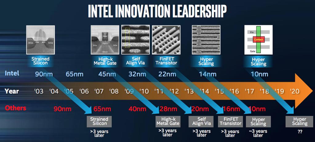
 8-Core chip (32 nm) to be introduced 2012. Serial data links operating at 10 Gbits/sec. Introduces 22 nm Tri-gate Transistor Tech.")
20 Moore s Law Impact on Intel ucomputers Min Feature Size 2BT µp (Intel Itanium Tukwila) 4-Core chip (65 nm) introduced Q BT mp (Intel Itanium Poulson) 8-Core chip (32 nm) to be introduced Serial data links operating at 10 Gbits/sec. Introduces 22 nm Tri-gate Transistor Tech. Complexity - # transistors Double every Two Years 0.032um um YEAR 21
21 More Moore # Scaling! Geometrical Scaling " continued shrinking of horizontal and vertical physical feature sizes! Equivalent Scaling " 3-dimensional device structure improvements and new materials that affect the electrical performance of the chip even if no geometrical scaling! Design Equivalent Scaling " design technologies that enable high performance, low power, high reliability, low cost, and high design productivity even if neither geometrical nor equivalent scaling can be used 22


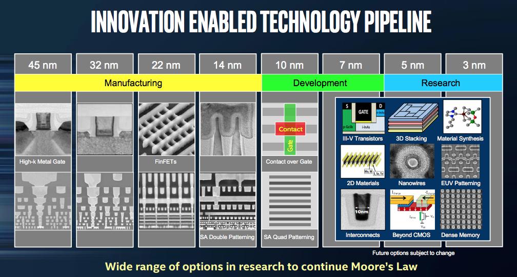
22 22nm 3D FinFET Transistor High-k gate dielectric Tri-Gate transistors with multiple fins connected together increases total drive strength for higher performance Details_Presentation.pdf 23
23 More Moore # Scaling! Examples: " Design-for-variability " Low power design (sleep modes, clock gating, multi- Vdd, etc.) " Multi-core SOC architectures 24
24 More than Moore # Functional Diversification! Interacting with the outside world " Electromagnetic/Optical " Radio-frequency domain up to the THz range " Optical domain from the infrared to the near ultraviolet " Hard radiation (EUV, X-ray, γ-ray) " Mechanical parameters (sensors/actuators) " MEMS/NEMS position, speed, acceleration, rotation, pressure, stress, etc. " Chemical composition (sensors/actuators) " Biological parameters (sensors/actuators)! Power/Energy " Integration of renewable sources, Energy storage, Smart metering, Efficient consumption 25

25 Scaling More-than-Moore More-than-Moore, International Road Map (IRC) White Paper, International Technology Roadmap for Semiconductors 26

26 More-than-Moore! Components Complement Digital Processing/ Storage Elements in an Integrated System 27


27 MicroImplant: An Electronic Platform for Minimally Invasive Sensory Monitors 28

28 Semiconductor System Integration More Than Moore's Law Transistors/cm SOP law for system integration. As components shrink and boards all but disappear, component density will double every year or so. Multichip Module Systemin-package (SIP) System on-package (SOP) Components/cm R. Tummala, Moore's Law Meets Its Match, IEEE Spectrum, June,
29 Improvement Trends for VLSI SoCs Enabled by Geometrical and Equivalent Scaling! TRENDS:! Higher Integration level " exponentially increased number of components/ transistors per chip/package.! Performance Scaling " combination of Geometrical (shrinking of dimensions) and Equivalent (innovation) Scaling.! System implementation " SoC + increased use of SiP - > SOP! CONSEQUENCES:! Higher Speed " CPU clock rate at multiple GHz + parallel processing.! Increased Compactness & less weight " increasing system integration.! Lower Power " Decreasing energy requirement per function.! Lower Cost " Decreasing cost per function. 30
 31")
30 Trends in Practice at ISSCC (HW 1) 31

31 Societal Needs 32
32 ITRS 2.0 Report 2015! After 2021, the report forecasts, it will no longer be economically desirable for companies to continue traditional transistor miniaturization in microprocessors. 33
33 BUT Source: 34
34 BUT Source: 35
35 Design Example
36 VLSI Design Cycle or Flow Verilog/SPICE 37
37 Illustrative Circuit Design Example: System Requirements Design a One-Bit Adder Circuit using 0.8 twin-well CMOS Technology. The design specifications are: 1. Propagation Delay Times of SUM and CARRY_Out signals: 1.2 ns 2. Rise and Fall Times of SUM and CARRY_Out signals: 1.2 ns 3. Circuit Die Area: 1500 um 2 4. Dynamic Power Dissipation (@ V DD = 5 V and f max = 20 MHz): 1 mw 5. Functional: 38
38 Illustrative Circuit Design Example: Architecture Definition 39
39 Illustrative Circuit Design Example: Logic Design! Gate Level Schematic of One-Bit Full Adder Circuit 40
40 Illustrative Circuit Design Example: VLSI Design! Transistor Level Schematic of One-Bit Full Adder Circuit 41
41 Illustrative Circuit Design Example: VLSI Design! 8-bit Ripple Adder 42

42 Illustrative Circuit Design Example: VLSI Design and Layout COUT SUMOUT N1 N2 COU T N1 N2 43

43 Illustrative Circuit Design Example: VLSI Design and Layout! Initial Layout of One-Bit Full Adder Circuit COU T 1500 um 2 Dynamic Power Dissipation (@ V DD = 5V, f max = 20 MHz): = 0.7 mw 1 mw 44
44 Illustrative Circuit Design Example: Design Verification Spec NOT met 45
45 Admin! Find web, get text, assigned reading " " " HW 1 posted now " Due next week 1/18! Remaining Questions? 46
Kenneth R. Laker, University of Pennsylvania, updated 20Jan15
 http://www.seas.upenn.edu/~ese570/ 1 TOPICS The Course Industry Trends Digital CMOS Basics Some VLSI Fundamentals Illustrative Design Example 2 1. Apply principles of hierarchical digital CMOS VLSI, from
! Review: MOS IV Curves and Switch Model. ! MOS Device Layout. ! Inverter Layout. ! Gate Layout and Stick Diagrams. ! Design Rules. !
 ESE 570: Digital Integrated Circuits and VLSI Fundamentals Lec 3: January 21, 2017 MOS Fabrication pt. 2: Design Rules and Layout Lecture Outline! Review: MOS IV Curves and Switch Model! MOS Device Layout!
Practical Information
 EE241 - Spring 2013 Advanced Digital Integrated Circuits MW 2-3:30pm 540A/B Cory Practical Information Instructor: Borivoje Nikolić 509 Cory Hall, 3-9297, bora@eecs Office hours: M 11-12, W 3:30pm-4:30pm
Practical Information
 EE241 - Spring 2010 Advanced Digital Integrated Circuits TuTh 3:30-5pm 293 Cory Practical Information Instructor: Borivoje Nikolić 550B Cory Hall, 3-9297, bora@eecs Office hours: M 10:30am-12pm Reader:
ESE 570: Digital Integrated Circuits and VLSI Fundamentals
 ESE 570: Digital Integrated Circuits and VLSI Fundamentals Lec 23: April 12, 2016 VLSI Design and Variation Penn ESE 570 Spring 2016 Khanna Lecture Outline! Design Methodologies " Hierarchy, Modularity,
! Analog VLSI Circuit Design. ! Convex Optimization. " System Hierarchical Optimization. ! Biomedical Electronics. ! Biometric Data Acquisition
 Where I come from ESE 531: Digital Signal Processing Lec 1: January 12, 2017 Introduction and Overview! Analog VLSI Circuit Design! Convex Optimization " System Hierarchical Optimization! Biomedical Electronics!
ESE 531: Digital Signal Processing
 ESE 531: Digital Signal Processing Lec 1: January 12, 2017 Introduction and Overview Where I come from! Analog VLSI Circuit Design! Convex Optimization " System Hierarchical Optimization! Biomedical Electronics!
ESE 531: Digital Signal Processing
 ESE 531: Digital Signal Processing Lec 1: January 17, 2019 Introduction and Overview Lecture Outline! Course Topics Overview! Learning Objectives! Course Structure! Course Policies! Course Content! What
ESE 570: Digital Integrated Circuits and VLSI Fundamentals
 ESE 570: Digital Integrated Circuits and VLSI Fundamentals Lec 3: January 24, 2019 MOS Fabrication pt. 2: Design Rules and Layout Penn ESE 570 Spring 2019 Khanna Jack Keil Wolf Lecture http://www.ese.upenn.edu/about-ese/events/wolf.php
! Review: Sequential MOS Logic. " SR Latch. " D-Latch. ! Timing Hazards. ! Dynamic Logic. " Domino Logic. ! Charge Sharing Setup.
 ESE 570: Digital Integrated Circuits and VLSI Fundamentals Lec 9: March 29, 206 Timing Hazards and Dynamic Logic Lecture Outline! Review: Sequential MOS Logic " SR " D-! Timing Hazards! Dynamic Logic "
Jack Keil Wolf Lecture. ESE 570: Digital Integrated Circuits and VLSI Fundamentals. Lecture Outline. MOSFET N-Type, P-Type.
 ESE 570: Digital Integrated Circuits and VLSI Fundamentals Jack Keil Wolf Lecture Lec 3: January 24, 2019 MOS Fabrication pt. 2: Design Rules and Layout http://www.ese.upenn.edu/about-ese/events/wolf.php
EE4800 CMOS Digital IC Design & Analysis. Lecture 1 Introduction Zhuo Feng
 EE4800 CMOS Digital IC Design & Analysis Lecture 1 Introduction Zhuo Feng 1.1 Prof. Zhuo Feng Office: EERC 730 Phone: 487-3116 Email: zhuofeng@mtu.edu Class Website http://www.ece.mtu.edu/~zhuofeng/ee4800fall2010.html
Advanced Digital Integrated Circuits. Lecture 2: Scaling Trends. Announcements. No office hour next Monday. Extra office hour Tuesday 2-3pm
 EE241 - Spring 20 Advanced Digital Integrated Circuits Lecture 2: Scaling Trends and Features of Modern Technologies Announcements No office hour next Monday Extra office hour Tuesday 2-3pm 2 1 Outline
CMOS Technology for Computer Architects
 CMOS Technology for Computer Architects Lecture 1: Introduction Iakovos Mavroidis Giorgos Passas Manolis Katevenis FORTH-ICS (University of Crete) Course Contents Implementation of high-performance digital
Lecture 1. Tinoosh Mohsenin
 Lecture 1 Tinoosh Mohsenin Today Administrative items Syllabus and course overview Digital systems and optimization overview 2 Course Communication Email Urgent announcements Web page http://www.csee.umbc.edu/~tinoosh/cmpe650/
EECS150 - Digital Design Lecture 2 - CMOS
 EECS150 - Digital Design Lecture 2 - CMOS August 29, 2002 John Wawrzynek Fall 2002 EECS150 - Lec02-CMOS Page 1 Outline Overview of Physical Implementations CMOS devices Announcements/Break CMOS transistor
Low-Power VLSI. Seong-Ook Jung VLSI SYSTEM LAB, YONSEI University School of Electrical & Electronic Engineering
 Low-Power VLSI Seong-Ook Jung 2013. 5. 27. sjung@yonsei.ac.kr VLSI SYSTEM LAB, YONSEI University School of Electrical & Electronic Engineering Contents 1. Introduction 2. Power classification & Power performance
ECEN474/704: (Analog) VLSI Circuit Design Fall 2016
 VLSI Circuit Design Fall 2016") ECEN474/704: (Analog) VLSI Circuit Design Fall 2016 Lecture 1: Introduction Sam Palermo Analog & Mixed-Signal Center Texas A&M University Announcements Turn in your 0.18um NDA form by Thursday Sep 1 No
ECEN474/704: (Analog) VLSI Circuit Design Fall 2016 Lecture 1: Introduction Sam Palermo Analog & Mixed-Signal Center Texas A&M University Announcements Turn in your 0.18um NDA form by Thursday Sep 1 No
! Review: MOS IV Curves and Switch Model. ! MOS Device Layout. ! Inverter Layout. ! Gate Layout and Stick Diagrams. ! Design Rules. !
 ESE 570: Digital Integrated Circuits and VLSI Fundamentals Lec 3: January 21, 2016 MOS Fabrication pt. 2: Design Rules and Layout Lecture Outline! Review: MOS IV Curves and Switch Model! MOS Device Layout!
ESE 570: Digital Integrated Circuits and VLSI Fundamentals
 ESE 570: Digital Integrated Circuits and VLSI Fundamentals Lec 3: January 21, 2016 MOS Fabrication pt. 2: Design Rules and Layout Penn ESE 570 Spring 2016 Khanna Adapted from GATech ESE3060 Slides Lecture
A design of 16-bit adiabatic Microprocessor core
 194 A design of 16-bit adiabatic Microprocessor core Youngjoon Shin, Hanseung Lee, Yong Moon, and Chanho Lee Abstract A 16-bit adiabatic low-power Microprocessor core is designed. The processor consists
Introduction to Electronic Design Automation
 Introduction to Electronic Design Automation Jie-Hong Roland Jiang 江介宏 Department of Electrical Engineering National Taiwan University Spring 2014 1 Design Automation? 2 Course Info (1/4) Instructor Jie-Hong
EE5324. VLSI Design II
 EE5324 VLSI Design II Professor Chris H. Kim University of Minnesota Dept. of ECE www.umn.edu/~chriskim/ chriskim@umn.edu Practical Information Class webpage http://www.ece.umn.edu/class/ee5324 Instructor:
! MOS Device Layout. ! Inverter Layout. ! Gate Layout and Stick Diagrams. ! Design Rules. ! Standard Cells. ! CMOS Process Enhancements
 EE 570: igital Integrated Circuits and VLI Fundamentals Lec 3: January 18, 2018 MO Fabrication pt. 2: esign Rules and Layout Lecture Outline! MO evice Layout! Inverter Layout! Gate Layout and tick iagrams!
Datorstödd Elektronikkonstruktion
 Datorstödd Elektronikkonstruktion [Computer Aided Design of Electronics] Zebo Peng, Petru Eles and Gert Jervan Embedded Systems Laboratory IDA, Linköping University http://www.ida.liu.se/~tdts80/~tdts80
Lecture 4&5 CMOS Circuits
 Lecture 4&5 CMOS Circuits Xuan Silvia Zhang Washington University in St. Louis http://classes.engineering.wustl.edu/ese566/ Worst-Case V OL 2 3 Outline Combinational Logic (Delay Analysis) Sequential Circuits
Lecture 0: Introduction
 Lecture 0: Introduction Introduction Integrated circuits: many transistors on one chip. Very Large Scale Integration (VLSI): bucketloads! Complementary Metal Oxide Semiconductor Fast, cheap, low power
Lecture #29. Moore s Law
 Lecture #29 ANNOUNCEMENTS HW#15 will be for extra credit Quiz #6 (Thursday 5/8) will include MOSFET C-V No late Projects will be accepted after Thursday 5/8 The last Coffee Hour will be held this Thursday
DIGITAL INTEGRATED CIRCUITS A DESIGN PERSPECTIVE 2 N D E D I T I O N
 DIGITAL INTEGRATED CIRCUITS A DESIGN PERSPECTIVE 2 N D E D I T I O N Jan M. Rabaey, Anantha Chandrakasan, and Borivoje Nikolic CONTENTS PART I: THE FABRICS Chapter 1: Introduction (32 pages) 1.1 A Historical
Course Content. Course Content. Course Format. Low Power VLSI System Design Lecture 1: Introduction. Course focus
 Course Content Low Power VLSI System Design Lecture 1: Introduction Prof. R. Iris Bahar E September 6, 2017 Course focus low power and thermal-aware design digital design, from devices to architecture
EECS 270 Schedule and Syllabus for Fall 2011 Designed by Prof. Pinaki Mazumder
 EECS 270 Schedule and Syllabus for Fall 2011 Designed by Prof. Pinaki Mazumder Week Day Date Lec No. Lecture Topic Textbook Sec Course-pack HW (Due Date) Lab (Start Date) 1 W 7-Sep 1 Course Overview, Number
420 Intro to VLSI Design
 Dept of Electrical and Computer Engineering 420 Intro to VLSI Design Lecture 0: Course Introduction and Overview Valencia M. Joyner Spring 2005 Getting Started Syllabus About the Instructor Labs, Problem
EECS150 - Digital Design Lecture 28 Course Wrap Up. Recap 1
 EECS150 - Digital Design Lecture 28 Course Wrap Up Dec. 5, 2013 Prof. Ronald Fearing Electrical Engineering and Computer Sciences University of California, Berkeley (slides courtesy of Prof. John Wawrzynek)
EE241 - Spring 2013 Advanced Digital Integrated Circuits. Announcements. Sign up for Piazza if you haven t already
 EE241 - Spring 2013 Advanced Digital Integrated Circuits Lecture 2: Scaling Trends and Features of Modern Technologies Announcements Sign up for Piazza if you haven t already 2 1 Assigned Reading R.H.
Intel's 65 nm Logic Technology Demonstrated on 0.57 µm 2 SRAM Cells
 Intel's 65 nm Logic Technology Demonstrated on 0.57 µm 2 SRAM Cells Mark Bohr Intel Senior Fellow Director of Process Architecture & Integration Intel 1 What are We Announcing? Intel has fabricated fully-functional
Trends and Challenges in VLSI Technology Scaling Towards 100nm
 Trends and Challenges in VLSI Technology Scaling Towards 100nm Stefan Rusu Intel Corporation stefan.rusu@intel.com September 2001 Stefan Rusu 9/2001 2001 Intel Corp. Page 1 Agenda VLSI Technology Trends
EE141-Spring 2007 Digital Integrated Circuits
 EE141-Spring 2007 Digital Integrated Circuits Lecture 22 I/O, Power Distribution dders 1 nnouncements Homework 9 has been posted Due Tu. pr. 24, 5pm Project Phase 4 (Final) Report due Mo. pr. 30, noon
! Is it feasible? ! How do we decompose the problem? ! Vdd. ! Topology. " Gate choice, logical optimization. " Fanin, fanout, Serial vs.
 ESE 570: Digital Integrated Circuits and VLSI Fundamentals Design Space Exploration Lec 18: March 28, 2017 Design Space Exploration, Synchronous MOS Logic, Timing Hazards 3 Design Problem Problem Solvable!
Progress due to: Feature size reduction - 0.7X/3 years (Moore s Law). Increasing chip size - 16% per year. Creativity in implementing functions.
. Increasing chip size - 16% per year. Creativity in implementing functions.") Introduction - Chapter 1 Evolution of IC Fabrication 1960 and 1990 integrated t circuits. it Progress due to: Feature size reduction - 0.7X/3 years (Moore s Law). Increasing chip size - 16% per year. Creativity
Introduction - Chapter 1 Evolution of IC Fabrication 1960 and 1990 integrated t circuits. it Progress due to: Feature size reduction - 0.7X/3 years (Moore s Law). Increasing chip size - 16% per year. Creativity
Digital Design and System Implementation. Overview of Physical Implementations
 Digital Design and System Implementation Overview of Physical Implementations CMOS devices CMOS transistor circuit functional behavior Basic logic gates Transmission gates Tri-state buffers Flip-flops
Interconnect-Power Dissipation in a Microprocessor
 4/2/2004 Interconnect-Power Dissipation in a Microprocessor N. Magen, A. Kolodny, U. Weiser, N. Shamir Intel corporation Technion - Israel Institute of Technology 4/2/2004 2 Interconnect-Power Definition
EMT 251 Introduction to IC Design
 EMT 251 Introduction to IC Design (Pengantar Rekabentuk Litar Terkamir) Semester II 2011/2012 Introduction to IC design and Transistor Fundamental Some Keywords! Very-large-scale-integration (VLSI) is
Introduction to VLSI ASIC Design and Technology
 Introduction to VLSI ASIC Design and Technology Paulo Moreira CERN - Geneva, Switzerland Paulo Moreira Introduction 1 Outline Introduction Is there a limit? Transistors CMOS building blocks Parasitics
ECE 484 VLSI Digital Circuits Fall Lecture 02: Design Metrics
 ECE 484 VLSI Digital Circuits Fall 2016 Lecture 02: Design Metrics Dr. George L. Engel Adapted from slides provided by Mary Jane Irwin (PSU) [Adapted from Rabaey s Digital Integrated Circuits, 2002, J.
Disseny físic. Disseny en Standard Cells. Enric Pastor Rosa M. Badia Ramon Canal DM Tardor DM, Tardor
 Disseny físic Disseny en Standard Cells Enric Pastor Rosa M. Badia Ramon Canal DM Tardor 2005 DM, Tardor 2005 1 Design domains (Gajski) Structural Processor, memory ALU, registers Cell Device, gate Transistor
EECS240 Spring Advanced Analog Integrated Circuits Lecture 1: Introduction. Elad Alon Dept. of EECS
 EECS240 Spring 2009 Advanced Analog Integrated Circuits Lecture 1: Introduction Elad Alon Dept. of EECS Course Focus Focus is on analog design Typically: Specs circuit topology layout Will learn spec-driven
CS 6135 VLSI Physical Design Automation Fall 2003
 CS 6135 VLSI Physical Design Automation Fall 2003 1 Course Information Class time: R789 Location: EECS 224 Instructor: Ting-Chi Wang ( ) EECS 643, (03) 5742963 tcwang@cs.nthu.edu.tw Office hours: M56R5
! Sequential Logic. ! Timing Hazards. ! Dynamic Logic. ! Add state elements (registers, latches) ! Compute. " From state elements
 ! Compute. From state elements") ESE 570: Digital Integrated Circuits and VLSI Fundamentals Lec 19: April 2, 2019 Sequential Logic, Timing Hazards and Dynamic Logic Lecture Outline! Sequential Logic! Timing Hazards! Dynamic Logic 4 Sequential
ESE 570: Digital Integrated Circuits and VLSI Fundamentals Lec 19: April 2, 2019 Sequential Logic, Timing Hazards and Dynamic Logic Lecture Outline! Sequential Logic! Timing Hazards! Dynamic Logic 4 Sequential
Domino CMOS Implementation of Power Optimized and High Performance CLA adder
 Domino CMOS Implementation of Power Optimized and High Performance CLA adder Kistipati Karthik Reddy 1, Jeeru Dinesh Reddy 2 1 PG Student, BMS College of Engineering, Bull temple Road, Bengaluru, India
ELCN100 Electronic Lab. Instruments and Measurements Spring Lecture 01: Introduction
 ELCN100 Electronic Lab. Instruments and Measurements Spring 2018 Lecture 01: Introduction Dr. Hassan Mostafa حسن مصطفى د. hmostafa@uwaterloo.ca LAB 1 Cairo University Course Outline Course objectives To
ECEN474: (Analog) VLSI Circuit Design Fall 2011
 VLSI Circuit Design Fall 2011") ECEN474: (Analog) VLSI Circuit Design Fall 2011 Lecture 1: Introduction Sebastian Hoyos Analog & Mixed-Signal Center Texas A&M University Analog Circuit Sequence 326 2 Why is Analog Important? [Silva]
ECEN474: (Analog) VLSI Circuit Design Fall 2011 Lecture 1: Introduction Sebastian Hoyos Analog & Mixed-Signal Center Texas A&M University Analog Circuit Sequence 326 2 Why is Analog Important? [Silva]
POWER EFFICIENT DESIGN OF COUNTER ON.12 MICRON TECHNOLOGY
 Volume-, Issue-, March 2 POWER EFFICIENT DESIGN OF COUNTER ON.2 MICRON TECHNOLOGY Simmy Hirkaney, Sandip Nemade, Vikash Gupta Abstract As chip manufacturing technology is suddenly on the threshold of major
International Journal of Scientific & Engineering Research, Volume 4, Issue 5, May ISSN
 International Journal of Scientific & Engineering Research, Volume 4, Issue 5, May-2013 2190 Biquad Infinite Impulse Response Filter Using High Efficiency Charge Recovery Logic K.Surya 1, K.Chinnusamy
Study the Analysis of Low power and High speed CMOS Logic Circuits in 90nm Technology
 43 Study the Analysis of Low power and High speed CMOS Logic Circuits in 90nm Technology Fazal Noorbasha 1, Ashish Verma 1 and A.M. Mahajan 2 1. Laboratory of VLSI and Embedded Systems, Deptt. Of Physics
Course Outcome of M.Tech (VLSI Design)
") Course Outcome of M.Tech (VLSI Design) PVL108: Device Physics and Technology The students are able to: 1. Understand the basic physics of semiconductor devices and the basics theory of PN junction. 2.
Course Outcome of M.Tech (VLSI Design) PVL108: Device Physics and Technology The students are able to: 1. Understand the basic physics of semiconductor devices and the basics theory of PN junction. 2.
EECS 151/251A Spring 2019 Digital Design and Integrated Circuits. Instructors: Wawrzynek. Lecture 8 EE141
 EECS 151/251A Spring 2019 Digital Design and Integrated Circuits Instructors: Wawrzynek Lecture 8 EE141 From the Bottom Up IC processing CMOS Circuits (next lecture) EE141 2 Overview of Physical Implementations
Lecture Outline. ESE 570: Digital Integrated Circuits and VLSI Fundamentals. Previously: Two XOR Gates. Pass Transistor Logic. Cascaded Pass Gates
 ESE 570: Digital Integrated Circuits and VLSI Fundamentals Lecture Outline! Pass Transistor Logic! Performance Lec 15: March 2, 2017 Combination Logic: Pass Transistor Logic, and Performance 2 Previously:
DIGITAL INTEGRATED CIRCUITS FALL 2003 ANALYSIS AND DESIGN OF DIGITAL INTEGRATED CIRCUITS (18-322) COURSE SYLLABUS
 COURSE SYLLABUS") ANALYSIS AND DESIGN OF DIGITAL INTEGRATED CIRCUITS (18-322) COURSE SYLLABUS Prof. Herman Schmit HH 2108; x 86470 herman@ece.cmu.edu Prof. Andrzej J. Strojwas HH 2106; X 83530 ajs@ece.cmu.edu 1 I. PURPOSE
ANALYSIS AND DESIGN OF DIGITAL INTEGRATED CIRCUITS (18-322) COURSE SYLLABUS Prof. Herman Schmit HH 2108; x 86470 herman@ece.cmu.edu Prof. Andrzej J. Strojwas HH 2106; X 83530 ajs@ece.cmu.edu 1 I. PURPOSE
EECS150 - Digital Design Lecture 19 CMOS Implementation Technologies. Recap and Outline
 EECS150 - Digital Design Lecture 19 CMOS Implementation Technologies Oct. 31, 2013 Prof. Ronald Fearing Electrical Engineering and Computer Sciences University of California, Berkeley (slides courtesy
Homework 10 posted just for practice. Office hours next week, schedule TBD. HKN review today. Your feedback is important!
 EE141 Fall 2005 Lecture 26 Memory (Cont.) Perspectives Administrative Stuff Homework 10 posted just for practice No need to turn in Office hours next week, schedule TBD. HKN review today. Your feedback
I/O Design EE141. Announcements. EE141-Fall 2006 Digital Integrated Circuits. Class Material. Pads + ESD Protection.
 EE141-Fall 2006 Digital Integrated Circuits nnouncements Homework 9 due on Thursday Lecture 26 I/O 1 2 Class Material Last lecture Timing Clock distribution Today s lecture I/O Power distribution Intro
Lecture Outline. ESE 570: Digital Integrated Circuits and VLSI Fundamentals. Teaser. Pass Transistor Logic. Identify Function.
 ESE 570: Digital Integrated Circuits and VLSI Fundamentals Lecture Outline! Pass Transistor Logic! Performance Lec 15: March 1, 2018 Combination Logic: Pass Transistor Logic, and Performance 2 Pass Transistor
Low Power 8-Bit ALU Design Using Full Adder and Multiplexer
 Low Power 8-Bit ALU Design Using Full Adder and Multiplexer Gaddam Sushil Raj B.Tech, Vardhaman College of Engineering. ABSTRACT: Arithmetic logic unit (ALU) is an important part of microprocessor. In
EE 434 ASIC & Digital Systems
 EE 434 ASIC & Digital Systems Dae Hyun Kim EECS Washington State University Spring 2017 Course Website http://eecs.wsu.edu/~ee434 Themes Study how to design, analyze, and test a complex applicationspecific
Computer Aided Design of Electronics
 Computer Aided Design of Electronics [Datorstödd Elektronikkonstruktion] Zebo Peng, Petru Eles, and Nima Aghaee Embedded Systems Laboratory IDA, Linköping University www.ida.liu.se/~tdts01 Electronic Systems
Technology Timeline. Transistors ICs (General) SRAMs & DRAMs Microprocessors SPLDs CPLDs ASICs. FPGAs. The Design Warrior s Guide to.
 SRAMs & DRAMs Microprocessors SPLDs CPLDs ASICs. FPGAs. The Design Warrior s Guide to.") FPGAs 1 CMPE 415 Technology Timeline 1945 1950 1955 1960 1965 1970 1975 1980 1985 1990 1995 2000 Transistors ICs (General) SRAMs & DRAMs Microprocessors SPLDs CPLDs ASICs FPGAs The Design Warrior s Guide
FPGAs 1 CMPE 415 Technology Timeline 1945 1950 1955 1960 1965 1970 1975 1980 1985 1990 1995 2000 Transistors ICs (General) SRAMs & DRAMs Microprocessors SPLDs CPLDs ASICs FPGAs The Design Warrior s Guide
Investigation on Performance of high speed CMOS Full adder Circuits
 ISSN (O): 2349-7084 International Journal of Computer Engineering In Research Trends Available online at: www.ijcert.org Investigation on Performance of high speed CMOS Full adder Circuits 1 KATTUPALLI
450mm and Moore s Law Advanced Packaging Challenges and the Impact of 3D
 450mm and Moore s Law Advanced Packaging Challenges and the Impact of 3D Doug Anberg VP, Technical Marketing Ultratech SOKUDO Lithography Breakfast Forum July 10, 2013 Agenda Next Generation Technology
Teaching Staff. EECS240 Spring Course Focus. Administrative. Course Goal. Lecture Notes. Elad s office hours
 EECS240 Spring 2012 Advanced Analog Integrated Circuits Lecture 1: Introduction Teaching Staff Elad s office hours 519 Cory Hall Tues. and Thurs. 11am-12pm (right after class) GSI: Pierluigi Nuzzo Weekly
Very Large Scale Integration (VLSI)
") Very Large Scale Integration (VLSI) Lecture 6 Dr. Ahmed H. Madian Ah_madian@hotmail.com Dr. Ahmed H. Madian-VLSI 1 Contents Array subsystems Gate arrays technology Sea-of-gates Standard cell Macrocell
Very Large Scale Integration (VLSI) Lecture 6 Dr. Ahmed H. Madian Ah_madian@hotmail.com Dr. Ahmed H. Madian-VLSI 1 Contents Array subsystems Gate arrays technology Sea-of-gates Standard cell Macrocell
A Novel Technique to Reduce Write Delay of SRAM Architectures
 A Novel Technique to Reduce Write Delay of SRAM Architectures SWAPNIL VATS AND R.K. CHAUHAN * Department of Electronics and Communication Engineering M.M.M. Engineering College, Gorahpur-73 010, U.P. INDIA
A NOVEL 4-Bit ARITHMETIC LOGIC UNIT DESIGN FOR POWER AND AREA OPTIMIZATION
 A NOVEL 4-Bit ARITHMETIC LOGIC UNIT DESIGN FOR POWER AND AREA OPTIMIZATION Mr. Snehal Kumbhalkar 1, Mr. Sanjay Tembhurne 2 Department of Electronics and Communication Engineering GHRAET, Nagpur, Maharashtra,
Lecture 1: Digital Systems and VLSI
 VLSI Design Lecture 1: Digital Systems and VLSI Shaahinhi Hessabi Department of Computer Engineering Sharif University of Technology Adapted with modifications from lecture notes prepared by the book author
Design Challenges in Multi-GHz Microprocessors
 Design Challenges in Multi-GHz Microprocessors Bill Herrick Director, Alpha Microprocessor Development www.compaq.com Introduction Moore s Law ( Law (the trend that the demand for IC functions and the
AN EFFICIENT APPROACH TO MINIMIZE POWER AND AREA IN CARRY SELECT ADDER USING BINARY TO EXCESS ONE CONVERTER
 AN EFFICIENT APPROACH TO MINIMIZE POWER AND AREA IN CARRY SELECT ADDER USING BINARY TO EXCESS ONE CONVERTER K. RAMAMOORTHY 1 T. CHELLADURAI 2 V. MANIKANDAN 3 1 Department of Electronics and Communication
Design of Low power and Area Efficient 8-bit ALU using GDI Full Adder and Multiplexer
 Design of Low power and Area Efficient 8-bit ALU using GDI Full Adder and Multiplexer Mr. Y.Satish Kumar M.tech Student, Siddhartha Institute of Technology & Sciences. Mr. G.Srinivas, M.Tech Associate
EE 330 Fall Sheng-Huang (Alex) Lee and Dan Congreve
 Lee and Dan Congreve") EE 330 Fall 2009 Integrated Electronics Lecture Instructor: Lab Instructors: Web Site: Lecture: MWF 9:00 Randy Geiger 2133 Coover rlgeiger@iastate.edu 294-7745 Sheng-Huang (Alex) Lee and Dan Congreve http://class.ece.iastate.edu/ee330/
EE 330 Fall 2009 Integrated Electronics Lecture Instructor: Lab Instructors: Web Site: Lecture: MWF 9:00 Randy Geiger 2133 Coover rlgeiger@iastate.edu 294-7745 Sheng-Huang (Alex) Lee and Dan Congreve http://class.ece.iastate.edu/ee330/
EE 280 Introduction to Digital Logic Design
 EE 280 Introduction to Digital Logic Design Lecture 1. Introduction EE280 Lecture 1 1-1 Instructors: EE 280 Introduction to Digital Logic Design Dr. Lukasz Kurgan (section A1) office: ECERF 6 th floor,
DESIGN & IMPLEMENTATION OF SELF TIME DUMMY REPLICA TECHNIQUE IN 128X128 LOW VOLTAGE SRAM
 DESIGN & IMPLEMENTATION OF SELF TIME DUMMY REPLICA TECHNIQUE IN 128X128 LOW VOLTAGE SRAM 1 Mitali Agarwal, 2 Taru Tevatia 1 Research Scholar, 2 Associate Professor 1 Department of Electronics & Communication
Overview. 1 Trends in Microprocessor Architecture. Computer architecture. Computer architecture
 Overview 1 Trends in Microprocessor Architecture R05 Robert Mullins Computer architecture Scaling performance and CMOS Where have performance gains come from? Modern superscalar processors The limits of
Low Power VLSI Circuit Synthesis: Introduction and Course Outline
 Low Power VLSI Circuit Synthesis: Introduction and Course Outline Ajit Pal Professor Department of Computer Science and Engineering Indian Institute of Technology Kharagpur INDIA -721302 Agenda Why Low
12-Bit 1-channel 4 MSPS ADC
 SPECIFICATION 1 FEATURES 12-Bit 1-channel 4 MSPS ADC TSMC CMOS 65 nm Resolution 12 bit Single power supplies for digital and analog parts (2.5 V) Sampling rate up to 4 MSPS Standby mode (current consumption
NanoFabrics: : Spatial Computing Using Molecular Electronics
 NanoFabrics: : Spatial Computing Using Molecular Electronics Seth Copen Goldstein and Mihai Budiu Computer Architecture, 2001. Proceedings. 28th Annual International Symposium on 30 June-4 4 July 2001
Lecture 04 CSE 40547/60547 Computing at the Nanoscale Interconnect
 Lecture 04 CSE 40547/60547 Computing at the Nanoscale Interconnect Introduction - So far, have considered transistor-based logic in the face of technology scaling - Interconnect effects are also of concern
CHAPTER 5 DESIGN AND ANALYSIS OF COMPLEMENTARY PASS- TRANSISTOR WITH ASYNCHRONOUS ADIABATIC LOGIC CIRCUITS
 70 CHAPTER 5 DESIGN AND ANALYSIS OF COMPLEMENTARY PASS- TRANSISTOR WITH ASYNCHRONOUS ADIABATIC LOGIC CIRCUITS A novel approach of full adder and multipliers circuits using Complementary Pass Transistor
EECS150 - Digital Design Lecture 15 - CMOS Implementation Technologies. Overview of Physical Implementations
 EECS150 - Digital Design Lecture 15 - CMOS Implementation Technologies Mar 12, 2013 John Wawrzynek Spring 2013 EECS150 - Lec15-CMOS Page 1 Overview of Physical Implementations Integrated Circuits (ICs)
EECS150 - Digital Design Lecture 9 - CMOS Implementation Technologies
 EECS150 - Digital Design Lecture 9 - CMOS Implementation Technologies Feb 14, 2012 John Wawrzynek Spring 2012 EECS150 - Lec09-CMOS Page 1 Overview of Physical Implementations Integrated Circuits (ICs)
Integrated Circuit Technology (Course Code: EE662) Lecture 1: Introduction
 Lecture 1: Introduction") Indian Institute of Technology Jodhpur, Year 2015 2016 Integrated Circuit Technology (Course Code: EE662) Lecture 1: Introduction Course Instructor: Shree Prakash Tiwari, Ph.D. Email: sptiwari@iitj.ac.in
Indian Institute of Technology Jodhpur, Year 2015 2016 Integrated Circuit Technology (Course Code: EE662) Lecture 1: Introduction Course Instructor: Shree Prakash Tiwari, Ph.D. Email: sptiwari@iitj.ac.in
Advanced FPGA Design. Tinoosh Mohsenin CMPE 491/691 Spring 2012
 Advanced FPGA Design Tinoosh Mohsenin CMPE 491/691 Spring 2012 Today Administrative items Syllabus and course overview Digital signal processing overview 2 Course Communication Email Urgent announcements
Leading at the edge TECHNOLOGY AND MANUFACTURING DAY
 Leading at the edge 22FFL technology MARK BOHR Intel Senior Fellow, Technology and Manufacturing Group Director, Process Architecture and Integration Disclosures Intel Technology and Manufacturing Day
ISSCC 2003 / SESSION 1 / PLENARY / 1.1
 ISSCC 2003 / SESSION 1 / PLENARY / 1.1 1.1 No Exponential is Forever: But Forever Can Be Delayed! Gordon E. Moore Intel Corporation Over the last fifty years, the solid-state-circuits industry has grown
Subthreshold Voltage High-k CMOS Devices Have Lowest Energy and High Process Tolerance
 Subthreshold Voltage High-k CMOS Devices Have Lowest Energy and High Process Tolerance Muralidharan Venkatasubramanian Auburn University vmn0001@auburn.edu Vishwani D. Agrawal Auburn University vagrawal@eng.auburn.edu
In 1951 William Shockley developed the world first junction transistor. One year later Geoffrey W. A. Dummer published the concept of the integrated
 Objectives History and road map of integrated circuits Application specific integrated circuits Design flow and tasks Electric design automation tools ASIC project MSDAP In 1951 William Shockley developed
FPGA Based System Design
 FPGA Based System Design Reference Wayne Wolf, FPGA-Based System Design Pearson Education, 2004 Why VLSI? Integration improves the design: higher speed; lower power; physically smaller. Integration reduces
VLSI Design I; A. Milenkovic 1
 CPE/EE 427, CPE 527 VLSI Design I L02: Design Metrics Department of Electrical and Computer Engineering University of Alabama in Huntsville Aleksandar Milenkovic ( www.ece.uah.edu/~milenka ) www.ece.uah.edu/~milenka/cpe527-03f
Effect of Aging on Power Integrity of Digital Integrated Circuits
 Effect of Aging on Power Integrity of Digital Integrated Circuits A. Boyer, S. Ben Dhia Alexandre.boyer@laas.fr Sonia.bendhia@laas.fr 1 May 14 th, 2013 Introduction and context Long time operation Harsh
+1 (479)
") Introduction to VLSI Design http://csce.uark.edu +1 (479) 575-6043 yrpeng@uark.edu Invention of the Transistor Vacuum tubes ruled in first half of 20th century Large, expensive, power-hungry, unreliable
Introduction to VLSI Design http://csce.uark.edu +1 (479) 575-6043 yrpeng@uark.edu Invention of the Transistor Vacuum tubes ruled in first half of 20th century Large, expensive, power-hungry, unreliable
University of Minnesota, Minneapolis, MN 2. Intel Corporation, Hillsboro, OR 3. Los Alamos National Laboratory, Los Alamos, NM
 Statistical Characterization of Radiation- Induced Pulse Waveforms and Flip-Flop Soft Errors in 14nm Tri-Gate CMOS Using a Back- Sampling Chain (BSC) Technique Saurabh Kumar 1, M. Cho 2, L. Everson 1,
A Low-Power 12 Transistor Full Adder Design using 3 Transistor XOR Gates
 A Low-Power 12 Transistor Full Adder Design using 3 Transistor XOR Gates Anil Kumar 1 Kuldeep Singh 2 Student Assistant Professor Department of Electronics and Communication Engineering Guru Jambheshwar
Electrical Engineering 40 Introduction to Microelectronic Circuits
 Electrical Engineering 40 Introduction to Microelectronic Circuits Instructor: Prof. Andy Neureuther EECS Department University of California, Berkeley Lecture 1, Slide 1 Introduction Instructor: Prof.