Kenneth R. Laker, University of Pennsylvania, updated 20Jan15
|
|
|
- Bridget Summers
- 5 years ago
- Views:
Transcription

1 1
2 TOPICS The Course Industry Trends Digital CMOS Basics Some VLSI Fundamentals Illustrative Design Example 2
3 1. Apply principles of hierarchical digital CMOS VLSI, from the transistor up to the system level, to the understanding of CMOS circuits and systems that are suitable for CMOS fabrication. 2. Apply the models for state-of-the-art VLSI components, fabrication steps, hierarchical design flow and semiconductor business economics to judge the manufacturability of a design and estimate its manufacturing costs. 3. Design simulated experiments using Cadence to verify the integrity of a CMOS circuit and its layout. 4. Design digital circuits that are manufacturable in CMOS. 5. Apply the Cadence VLSI CAD tool suite layout digital circuits for CMOS fabrication and verify said circuits with layout parasitic elements. 6. Apply course knowledge and the Cadence VLSI CAD tools in a team based capstone design project that involves much the same design flow they would encounter in a semiconductor design industrial setting. Capstone project is presented in a formal report due at the end of the semester. 3
4 Classification of Digital CMOS Circuits STATIC CIRCUITS DYNAMIC CIRCUITS STATIC CIRCUIT In steady-state the output is always at a 1 or 0 via a lowimpedance path between the output and VDD or GND, respectively. DYNAMIC CIRCUIT In steady-state the output is at 1 or 0 due to the presence or absence of charge, respectively, stored on the output node capacitance. 4
5 Course Introduction 5
6 COURSE PROTOCOLS Grading Policies Homework: 20 % Midterm 05Mar15: 40 % Project 07May15: 40 % Homework Policies Homework assignments are combination of textbook problems, CADENCE tutorial & CADENCE lab exercises. Homework is assigned each week by Friday and will be due on Thursday the week after it is assigned. All homework assignments and due dates will be posted on the ESE 570 website Students are permitted up to THREE one-week latenesses without penalty. a. On three occasions homework may be turned-in one week after the official due date, unless it falls on a university or religious holiday. b. Homework not turned in accordance with policy will receive zero grade. 6
7 Industry Trends 7
8 Microprocessor Transistor Count & Moore's Law 16-Core SPARC T3 10-Core Xenon 6-Core 6-Core i7 i7 IBM 4-Core z196 2-Core Itanium 2 IBM 8-Core POWER7 4-Core Itanium Tukwilla AMD K10 AMD 6-Core Opteron Core i7 Curve shows transistor count doubling every two years Pentium AMD K8 Pentium 4 AMD K7 Pentium III Pentium II AMD K Mot Mot Zilog Z MOS : Oracle SPARC M7, 20 nm CMOS, 32-Core, 10B 3-D FinFET transistors

9 TREND Minimum Feature Size vs Year Process Node/ Minimum Feature 100 µm Integrated Circuit History 10 µm 1 µm ITRS Roadmap 0.18 µm in µm 10 nm Distant Future Transition Region 1 nm Quantum Devices 0.1 nm 1960 Atomic Dimensions Year Minimum Feature Measure = line/gate conductor width or half-pitch (adjacent 1st metal layer lines or adjacent transistor gates) 9
10 Intel Cost Scaling 10


11 22 nm 3-D FinFET Transistor High-k gate dielectric Tri-Gate transistors with multiple fins connected together increases total drive strength for higher performance 11

12 Moore's Law Impact on Intel Micro-Computers 2BT µp (Intel Itanium Tukwila) 4-Core chip (65 nm) introduced Q BT mp (Intel Itanium Poulson) 8-Core chip (32 nm) to be introduced Serial data22 links at 10 Gbits/sec. Introduces nm operating Tri-gate Transistor Tech. Increased reuse of logic IP, i.e. designs and cores. Complexity - # transistors Double every Two Years ' m ' m YEAR 12
 White Paper, 2011.")
13 Moore's Law and More Geometrical g ScalinScaling Equivalent Scaling More-than-Moore, International Road Map (IRC) White Paper, International Technology Road Map for Semiconductors 13
14 More Moore => Scaling Geometrical Scaling - refers to the continued shrinking of horizontal and vertical physical feature sizes. Equivalent Scaling - refers to 3-dimensional device structure improvements and new materials that affect the electrical performance of the chip even if no geometrical scaling. Design Equivalent Scaling - refers to design technologies that enable high performance, low power, high reliability, low cost, and high design productivity even if neither geometrical nor equivalent scaling can be used. Examples include: Design-for-variability Low power design (sleep modes, clock gating, multi-vdd, etc.) Multi-core SOC architectures 14
15 Examples of More Than Moore Devices More than Moore => Functional Diversification Interacting with the outside world Electromagnetic/Optical - Radio-frequency domain up to the THz range - Optical domain from the infrared to the near ultraviolet - Hard radiation (EUV, X-ray, γ-ray) Mechanical parameters (sensors/actuators) - MEMS/NEMS position, speed, acceleration, rotation, pressure, stress, etc. Chemical composition (sensors/actuators) Biological parameters (sensors/actuators) Powering Integration of renewable sources Energy storage Smart metering Efficient consumption 15

16 More-than-Moore Components Complement Digital Processing/Storage Elements in an Integrated System 16
 Photodiode Array Readout Integrated Circuit (ROIC) Digital Signal Processing (DSP)")
17 3D integration of More-than-Moore photodetector with More Moore ROIC and DSP optical Back-Side Illuminated (BSI) Photodiode Array Readout Integrated Circuit (ROIC) Digital Signal Processing (DSP) electrical 17
 on-package Module (SOP) 102 103 102 10 10 1970 Components/cm2 Transistors/cm2 108 1010 1980 1990 2000 2010 2020 R.")
18 Semiconductor System Integration More Than Moore's Law SOP law for system integration. As components shrink and boards all but disappear, component density will double every year or so Systemin-package System- 103 Multichip (SIP) on-package Module (SOP) Components/cm2 Transistors/cm R. Tummala, Moore's Law Meets Its Match, IEEE Spectrum, June,


19 System-on-Package Vision (Georgia Tech 3D Systems Packaging Research Center) 19
20 Improvement Trends for VLSI SoCs Enabled by Geometrical and Equivalent Scaling TRENDS 1. Higher Integration level -> exponentially increased number of components/transistors per chip/package. 2. Performance Scaling -> combination of Geometrical (shrinking of dimensions) and Equivalent (innovation) Scaling. 3. System implementation -> SoC + increased use of SiP -> SOP CONSEQUENCES 4. Higher Speed -> CPU clock rate at multiple GHz + parallel processing. 5. Increased Compactness & less weight -> increasing system integration. 6. Lower Power -> Decreasing energy requirement per function. 7. Lower Cost -> Decreasing cost per function. 20
21 Digital CMOS Basics 21
22 Classification of Digital CMOS Circuits STATIC CIRCUITS DYNAMIC CIRCUITS STATIC CIRCUIT In steady-state the output is always at a 1 or 0 via a lowimpedance path between the output and VDD or GND, respectively. DYNAMIC CIRCUIT In steady-state the output is at 1 or 0 due to the presence or absence of charge, respectively, stored on the output node capacitance. 22
23 23
24 24
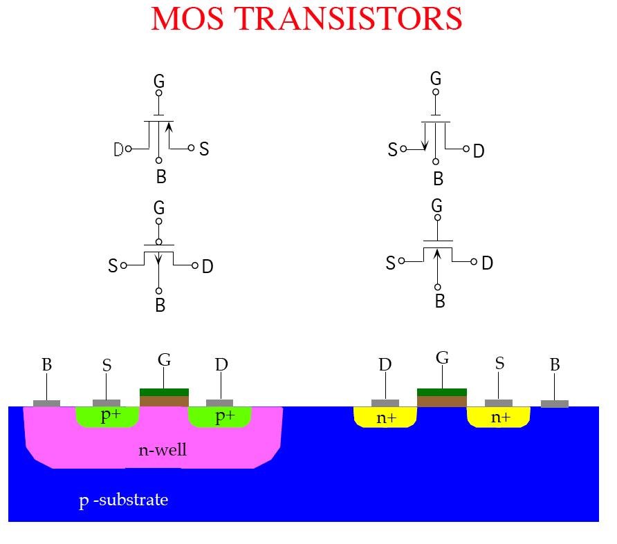
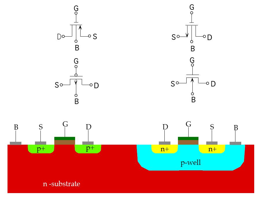
25 Ideal nmos and pmos Characteristics High Impedance or High Z g g=1 g=1 g=1 g a b g g=0 g b g=0 g=1 High Impedance or High Z a a b a g=0 a b g=0 If N- & P-Switch are MOS transistors a = drain & b = source 25
26 22 Complementary CMOS Switch -g g g -g -g g g 26
27 Ideal CMOS Inverter Inverter Truth Table PUN F=A F=A F=A A PDN F=A F=A 0 (GND) 27
28 F A? = N A F P 0 (GND) 0 (GND) 28
29 CMOS GATES VDD A B C D When the PUN is conducting, the output F will be 1. Hence,the PUN is determined by a Boolean expression for the un-complemented output F in terms of the complemented inputs (A,B,C,D). PUN Inputs F = f(a,b,c,d) A B C D PDN PUN and PDN are Dual Nets DeMorgan s Theorem Output When the PDN is conducting, the output F will be 0. Hence,the PDN is determined by a Boolean expression for the complemented output F in terms of the un-complemented inputs (A,B,C,D). 29
30 Two-Input CMOS NAND Gate DeMorgan's Theorem PUN F =% A$B& F =% A B& F A AND % A B & NOT % A B & = % A$B& OR % A$B& NOT B Gate Circuit Symbols F =% A B& PDN OUTPUT A-INPUT FF=% A B& A B-INPUT B Z = open circuit 30
31 Two-Input CMOS NOR Gate F PUN F =% A B& DeMorgan's Theorem % A$B& = % A B & B A % A$B& OR F F =% A$B& % A B & AND F =% A$B& PDN A $ B 31
32 Constructing Compound CMOS Gates F =%% A B&$%C D&& PUN (F = f(a,b,c,d) F =% A$B& %C $D& 1 X X 1 F X PUN PDN(F = f(a,b,c,d) F =%% A B&$%C D&& F 0 F F 0 F PDN 0 32
33 F =%% A B &$%C D&& Combining the PDN and PUN => 33
34 MULTIPLEXOR (MUX) output = A s$b s x = DON'T CARE 34
35 Some VLSI Fundamentals Oracle SPARC M7 Processor 35
36 VLSI Hierarchical Representations fabricated? - Circuit - Component 36
37 Y-Chart: Consistent Abstractions in 3 Domains System Level Algorithmic Level Behavioral Domain Register-Transfer Level Structural Domain System Specification CPU, ASIC Logic Level Algorithm Processor, Sub-system Register-Transfer Spec. ALU, Register, MUX Circuit Level Boolean Expression Gate/Flip-flop Transistor Model Equation Transistor symbols Transistor Layout Standard-cell/Sub-cell Layout Macro-cell/Module Layout Block/Die Layout Chip/SoC/Board Physical Domain 37
38 Goal of All VLSI Design Enterprises Convert System Specs into an IC DESIGN in MINIMUM TIME and with MAXIMUM LIKLIHOOD that the Design will PEFORM AS SPECIFIED when fabricated. MAX YIELD + MIN DEVELOPMENT TIME + MIN DIE AREA=> MIN COST TRADEOFFS MIN DIE AREA MIN DEVELOPMENT TIME MIN DIE AREA MAX YIELD 38

39 CMOS CHIP MANUFCTURING STEPS 39
40 Basic VLSI Chip Cost Model cost per packaged IC die = variable cost per IC packaged die + # good die FIXED COST: total cost due to expenditures that do not directly vary with sales, e.g. R&D, equipment depreciation, general operations and administration. mask set, all indirect costs. VARIABLE COST: total cost due to expenditures directly linked to making the product; e.g. engineering, wafer, mask set, test, package. variable cost variable cost per packaged = IC die (total # of die fabricated) * yield # good die # of IC dies satisfy ALL requirements total # of IC dies fabricated where 0 yield 1 (100 %) 40
41 VLSI Design Cycle or Flow Verilog/SPICE 41
42 Illustrative Circuit Design Example Design a One-Bit Adder Circuit using 00.8 (8µmtwin-well twin-wellcmos CMOSTechnology. technology. The The design specifications are: 1. Propagation Delay Times of SUM and CARRY_Out signals: 1.2 ns 2. Rise and Fall Times of SUM 2and CARRY_Out signals: 1.2 ns 3. Circuit Die Area: 1500 ' m 4. Dynamic Power Dissipation (@ VDD = 5 V and f max = 20 MHz): 1 mw 5. Functional 42
43 Bit-Sliced Data Path Control Bit N Data IN Data OUT Register ADDER Shifter Multiplier Bit 0 43
44 Illustrative Circuit Design Example Binary Full Adder (BFA) sum_out = A + B + C = ABC + ABC + ABC + ACB = ABC + (A + B + C) carry_out carry_out + AB + AC + BC Use of carry_out to realize sum_out reduces circuit complexity and die area. 44
45 Gate Level Schematic of One-Bit Full Adder Circuit NOT directly realizable in CMOS - Why? 45

46 8-bit Ripple Adder a<7:0> b<7:0> VDD BFA(0) cin BFA(1) BFA(2) BFA(7) cout clk GND 1-bit Adder Cell sum<7:0> a b vdd cin BFA cout gnd sum 46
47 42 Transistor Level Schematic of One-Bit Full Adder Circuit COUT % A$B & C $ A B COUT SUMOUT % A$B$C & COUT CMOS Implementable A B C$% A$B$C & COUT 47

48 Initial Layout of One-Bit Full Adder Circuit COUT N1 SUMOUT N2 COUT N1 N1 N2 N2 48
: = 0.")
49 Initial Layout of One-Bit Full Adder Circuit COUT 1500 ' m 2 Dynamic Power Dissipation (@ VDD = 5V, f max = 20 MHz): = 0.7 mw 1 mw 49
50 Simulated Performance of One-Bit Full Adder Circuit Let all specs be met except tplh, i.e. Spec NOT met. 50
ESE 570: Digital Integrated Circuits and VLSI Fundamentals
 ESE 570: Digital Integrated Circuits and VLSI Fundamentals Lec 1: January 11, 2018 Introduction and Overview Where I come from! Analog VLSI Circuit Design! Convex Optimization " System Hierarchical Optimization!
EECS150 - Digital Design Lecture 15 - CMOS Implementation Technologies. Overview of Physical Implementations
 EECS150 - Digital Design Lecture 15 - CMOS Implementation Technologies Mar 12, 2013 John Wawrzynek Spring 2013 EECS150 - Lec15-CMOS Page 1 Overview of Physical Implementations Integrated Circuits (ICs)
EECS150 - Digital Design Lecture 9 - CMOS Implementation Technologies
 EECS150 - Digital Design Lecture 9 - CMOS Implementation Technologies Feb 14, 2012 John Wawrzynek Spring 2012 EECS150 - Lec09-CMOS Page 1 Overview of Physical Implementations Integrated Circuits (ICs)
Chapter 3 Digital Logic Structures
 Chapter 3 Digital Logic Structures Transistor: Building Block of Computers Microprocessors contain millions of transistors Intel Pentium 4 (2000): 48 million IBM PowerPC 750FX (2002): 38 million IBM/Apple
EMT 251 Introduction to IC Design
 EMT 251 Introduction to IC Design (Pengantar Rekabentuk Litar Terkamir) Semester II 2011/2012 Introduction to IC design and Transistor Fundamental Some Keywords! Very-large-scale-integration (VLSI) is
Low-Power VLSI. Seong-Ook Jung VLSI SYSTEM LAB, YONSEI University School of Electrical & Electronic Engineering
 Low-Power VLSI Seong-Ook Jung 2013. 5. 27. sjung@yonsei.ac.kr VLSI SYSTEM LAB, YONSEI University School of Electrical & Electronic Engineering Contents 1. Introduction 2. Power classification & Power performance
CMOS Technology for Computer Architects
 CMOS Technology for Computer Architects Lecture 1: Introduction Iakovos Mavroidis Giorgos Passas Manolis Katevenis FORTH-ICS (University of Crete) Course Contents Implementation of high-performance digital
Introduction to VLSI ASIC Design and Technology
 Introduction to VLSI ASIC Design and Technology Paulo Moreira CERN - Geneva, Switzerland Paulo Moreira Introduction 1 Outline Introduction Is there a limit? Transistors CMOS building blocks Parasitics
EECS150 - Digital Design Lecture 19 CMOS Implementation Technologies. Recap and Outline
 EECS150 - Digital Design Lecture 19 CMOS Implementation Technologies Oct. 31, 2013 Prof. Ronald Fearing Electrical Engineering and Computer Sciences University of California, Berkeley (slides courtesy
Chapter 3 Digital Logic Structures
 Chapter 3 Digital Logic Structures Transistor: Building Block of Computers Microprocessors contain millions of transistors Intel Pentium 4 (2): 48 million IBM PowerPC 75FX (22): 38 million IBM/Apple PowerPC
Investigation on Performance of high speed CMOS Full adder Circuits
 ISSN (O): 2349-7084 International Journal of Computer Engineering In Research Trends Available online at: www.ijcert.org Investigation on Performance of high speed CMOS Full adder Circuits 1 KATTUPALLI
ECE 334: Electronic Circuits Lecture 10: Digital CMOS Circuits
 Faculty of Engineering ECE 334: Electronic Circuits Lecture 10: Digital CMOS Circuits CMOS Technology Complementary MOS, or CMOS, needs both PMOS and NMOS FET devices for their logic gates to be realized
A Low Power and Area Efficient Full Adder Design Using GDI Multiplexer
 A Low Power and Area Efficient Full Adder Design Using GDI Multiplexer G.Bramhini M.Tech (VLSI), Vidya Jyothi Institute of Technology. G.Ravi Kumar, M.Tech Assistant Professor, Vidya Jyothi Institute of
! Review: MOS IV Curves and Switch Model. ! MOS Device Layout. ! Inverter Layout. ! Gate Layout and Stick Diagrams. ! Design Rules. !
 ESE 570: Digital Integrated Circuits and VLSI Fundamentals Lec 3: January 21, 2017 MOS Fabrication pt. 2: Design Rules and Layout Lecture Outline! Review: MOS IV Curves and Switch Model! MOS Device Layout!
EECS150 - Digital Design Lecture 2 - CMOS
 EECS150 - Digital Design Lecture 2 - CMOS August 29, 2002 John Wawrzynek Fall 2002 EECS150 - Lec02-CMOS Page 1 Outline Overview of Physical Implementations CMOS devices Announcements/Break CMOS transistor
CHAPTER 3 NEW SLEEPY- PASS GATE
 56 CHAPTER 3 NEW SLEEPY- PASS GATE 3.1 INTRODUCTION A circuit level design technique is presented in this chapter to reduce the overall leakage power in conventional CMOS cells. The new leakage po leepy-
ECE 2300 Digital Logic & Computer Organization
 ECE 2300 Digital Logic & Computer Organization Spring 2018 CMOS Logic Lecture 4: 1 NAND Logic Gate X Y (X Y) = NAND Using De Morgan s Law: (X Y) = X +Y X X X +Y = Y Y Also a NAND We can build circuits
Implementation of Low Power High Speed Full Adder Using GDI Mux
 Implementation of Low Power High Speed Full Adder Using GDI Mux Thanuja Kummuru M.Tech Student Department of ECE Audisankara College of Engineering and Technology. Abstract The binary adder is the critical
Digital Design and System Implementation. Overview of Physical Implementations
 Digital Design and System Implementation Overview of Physical Implementations CMOS devices CMOS transistor circuit functional behavior Basic logic gates Transmission gates Tri-state buffers Flip-flops
Low Power 8-Bit ALU Design Using Full Adder and Multiplexer
 Low Power 8-Bit ALU Design Using Full Adder and Multiplexer Gaddam Sushil Raj B.Tech, Vardhaman College of Engineering. ABSTRACT: Arithmetic logic unit (ALU) is an important part of microprocessor. In
A new 6-T multiplexer based full-adder for low power and leakage current optimization
 A new 6-T multiplexer based full-adder for low power and leakage current optimization G. Ramana Murthy a), C. Senthilpari, P. Velrajkumar, and T. S. Lim Faculty of Engineering and Technology, Multimedia
Design of Low power and Area Efficient 8-bit ALU using GDI Full Adder and Multiplexer
 Design of Low power and Area Efficient 8-bit ALU using GDI Full Adder and Multiplexer Mr. Y.Satish Kumar M.tech Student, Siddhartha Institute of Technology & Sciences. Mr. G.Srinivas, M.Tech Associate
Power-Area trade-off for Different CMOS Design Technologies
 Power-Area trade-off for Different CMOS Design Technologies Priyadarshini.V Department of ECE Sri Vishnu Engineering College for Women, Bhimavaram dpriya69@gmail.com Prof.G.R.L.V.N.Srinivasa Raju Head
Study the Analysis of Low power and High speed CMOS Logic Circuits in 90nm Technology
 43 Study the Analysis of Low power and High speed CMOS Logic Circuits in 90nm Technology Fazal Noorbasha 1, Ashish Verma 1 and A.M. Mahajan 2 1. Laboratory of VLSI and Embedded Systems, Deptt. Of Physics
Design of 32-bit ALU using Low Power Energy Efficient Full Adder Circuits
 Design of 32-bit ALU using Low Power Energy Efficient Full Adder Circuits Priyadarshini.V Department of ECE Gudlavalleru Engieering College,Gudlavalleru darshiniv708@gmail.com Ramya.P Department of ECE
Introduction. Digital Integrated Circuits A Design Perspective. Jan M. Rabaey Anantha Chandrakasan Borivoje Nikolic. July 30, 2002
 Digital Integrated Circuits A Design Perspective Jan M. Rabaey Anantha Chandrakasan Borivoje Nikolic Introduction July 30, 2002 1 What is this book all about? Introduction to digital integrated circuits.
High Performance Low-Power Signed Multiplier
 High Performance Low-Power Signed Multiplier Amir R. Attarha Mehrdad Nourani VLSI Circuits & Systems Laboratory Department of Electrical and Computer Engineering University of Tehran, IRAN Email: attarha@khorshid.ece.ut.ac.ir
Introduction to Electronic Design Automation
 Introduction to Electronic Design Automation Jie-Hong Roland Jiang 江介宏 Department of Electrical Engineering National Taiwan University Spring 2014 1 Design Automation? 2 Course Info (1/4) Instructor Jie-Hong
EE4800 CMOS Digital IC Design & Analysis. Lecture 1 Introduction Zhuo Feng
 EE4800 CMOS Digital IC Design & Analysis Lecture 1 Introduction Zhuo Feng 1.1 Prof. Zhuo Feng Office: EERC 730 Phone: 487-3116 Email: zhuofeng@mtu.edu Class Website http://www.ece.mtu.edu/~zhuofeng/ee4800fall2010.html
420 Intro to VLSI Design
 Dept of Electrical and Computer Engineering 420 Intro to VLSI Design Lecture 0: Course Introduction and Overview Valencia M. Joyner Spring 2005 Getting Started Syllabus About the Instructor Labs, Problem
Jack Keil Wolf Lecture. ESE 570: Digital Integrated Circuits and VLSI Fundamentals. Lecture Outline. MOSFET N-Type, P-Type.
 ESE 570: Digital Integrated Circuits and VLSI Fundamentals Jack Keil Wolf Lecture Lec 3: January 24, 2019 MOS Fabrication pt. 2: Design Rules and Layout http://www.ese.upenn.edu/about-ese/events/wolf.php
Lecture 2: Digital Logic Basis
 Lecture 2: Digital Logic Basis Xufeng Kou School of Information Science and Technology ShanghaiTech University 1 Outline Truth Table Basic Logic Operation and Gates Logic Circuits NOR Gates and NAND Gates
Dr. Nicola Nicolici COE/EE2DI4 Midterm Test #1 Oct 18, 2006
 COE/EE2DI4 Midterm Test #1 Fall 2006 Page 1 Dr. Nicola Nicolici COE/EE2DI4 Midterm Test #1 Oct 18, 2006 Instructions: This examination paper includes 10 pages and 20 multiple-choice questions starting
ECE/CoE 0132: FETs and Gates
 ECE/CoE 0132: FETs and Gates Kartik Mohanram September 6, 2017 1 Physical properties of gates Over the next 2 lectures, we will discuss some of the physical characteristics of integrated circuits. We will
A HIGH SPEED & LOW POWER 16T 1-BIT FULL ADDER CIRCUIT DESIGN BY USING MTCMOS TECHNIQUE IN 45nm TECHNOLOGY
 A HIGH SPEED & LOW POWER 16T 1-BIT FULL ADDER CIRCUIT DESIGN BY USING MTCMOS TECHNIQUE IN 45nm TECHNOLOGY Jasbir kaur 1, Neeraj Singla 2 1 Assistant Professor, 2 PG Scholar Electronics and Communication
Datorstödd Elektronikkonstruktion
 Datorstödd Elektronikkonstruktion [Computer Aided Design of Electronics] Zebo Peng, Petru Eles and Gert Jervan Embedded Systems Laboratory IDA, Linköping University http://www.ida.liu.se/~tdts80/~tdts80
Leakage Power Reduction in 5-Bit Full Adder using Keeper & Footer Transistor
 Leakage Power Reduction in 5-Bit Full Adder using Keeper & Footer Transistor Narendra Yadav 1, Vipin Kumar Gupta 2 1 Department of Electronics and Communication, Gyan Vihar University, Jaipur, Rajasthan,
ESE 570: Digital Integrated Circuits and VLSI Fundamentals
 ESE 570: Digital Integrated Circuits and VLSI Fundamentals Lec 3: January 24, 2019 MOS Fabrication pt. 2: Design Rules and Layout Penn ESE 570 Spring 2019 Khanna Jack Keil Wolf Lecture http://www.ese.upenn.edu/about-ese/events/wolf.php
Low Power Design for Systems on a Chip. Tutorial Outline
 Low Power Design for Systems on a Chip Mary Jane Irwin Dept of CSE Penn State University (www.cse.psu.edu/~mji) Low Power Design for SoCs ASIC Tutorial Intro.1 Tutorial Outline Introduction and motivation
A Novel Approach for High Speed and Low Power 4-Bit Multiplier
 IOSR Journal of VLSI and Signal Processing (IOSR-JVSP) ISSN: 2319 4200, ISBN No. : 2319 4197 Volume 1, Issue 3 (Nov. - Dec. 2012), PP 13-26 A Novel Approach for High Speed and Low Power 4-Bit Multiplier
EC 1354-Principles of VLSI Design
 EC 1354-Principles of VLSI Design UNIT I MOS TRANSISTOR THEORY AND PROCESS TECHNOLOGY PART-A 1. What are the four generations of integrated circuits? 2. Give the advantages of IC. 3. Give the variety of
Lecture 0: Introduction
 Introduction to CMOS VLSI Design Lecture : Introduction David Harris Steven Levitan Harvey Mudd College University of Pittsburgh Spring 24 Fall 28 Administrivia Professor Steven Levitan TA: Bo Zhao Syllabus
Low Power 8-Bit ALU Design Using Full Adder and Multiplexer Based on GDI Technique
 Low Power 8-Bit ALU Design Using Full Adder and Multiplexer Based on GDI Technique Mohd Shahid M.Tech Student Al-Habeeb College of Engineering and Technology. Abstract Arithmetic logic unit (ALU) is an
Engr354: Digital Logic Circuits
 Engr354: Digital Logic Circuits Chapter 3: Implementation Technology Curtis Nelson Chapter 3 Overview In this chapter you will learn about: How transistors are used as switches; Integrated circuit technology;
Spiral 1 / Unit 8. Transistor Implementations CMOS Logic Gates
 18.1 Spiral 1 / Unit 8 Transistor Implementations CMOS Logic Gates 18.2 Spiral Content Mapping Spiral Theory Combinational Design Sequential Design System Level Design Implementation and Tools Project
ECE 410: VLSI Design Course Lecture Notes (Uyemura textbook)
") ECE 410: VLSI Design Course Lecture Notes (Uyemura tetbook) Professor Fathi Salem Michigan State University We will be updating the notes this Semester. Lecture Notes Page 2.1 Electronics Revolution Age
ECE 410: VLSI Design Course Lecture Notes (Uyemura tetbook) Professor Fathi Salem Michigan State University We will be updating the notes this Semester. Lecture Notes Page 2.1 Electronics Revolution Age
+1 (479)
") Introduction to VLSI Design http://csce.uark.edu +1 (479) 575-6043 yrpeng@uark.edu Invention of the Transistor Vacuum tubes ruled in first half of 20th century Large, expensive, power-hungry, unreliable
Introduction to VLSI Design http://csce.uark.edu +1 (479) 575-6043 yrpeng@uark.edu Invention of the Transistor Vacuum tubes ruled in first half of 20th century Large, expensive, power-hungry, unreliable
Disseny físic. Disseny en Standard Cells. Enric Pastor Rosa M. Badia Ramon Canal DM Tardor DM, Tardor
 Disseny físic Disseny en Standard Cells Enric Pastor Rosa M. Badia Ramon Canal DM Tardor 2005 DM, Tardor 2005 1 Design domains (Gajski) Structural Processor, memory ALU, registers Cell Device, gate Transistor
Lecture 0: Introduction
 Lecture 0: Introduction Introduction Integrated circuits: many transistors on one chip. Very Large Scale Integration (VLSI): bucketloads! Complementary Metal Oxide Semiconductor Fast, cheap, low power
Integration of Optimized GDI Logic based NOR Gate and Half Adder into PASTA for Low Power & Low Area Applications
 Integration of Optimized GDI Logic based NOR Gate and Half Adder into PASTA for Low Power & Low Area Applications M. Sivakumar Research Scholar, ECE Department, SCSVMV University, Kanchipuram, India. Dr.
CMOS VLSI IC Design. A decent understanding of all tasks required to design and fabricate a chip takes years of experience
 CMOS VLSI IC Design A decent understanding of all tasks required to design and fabricate a chip takes years of experience 1 Commonly used keywords INTEGRATED CIRCUIT (IC) many transistors on one chip VERY
A SUBSTRATE BIASED FULL ADDER CIRCUIT
 International Journal on Intelligent Electronic System, Vol. 8 No.. July 4 9 A SUBSTRATE BIASED FULL ADDER CIRCUIT Abstract Saravanakumar C., Senthilmurugan S.,, Department of ECE, Valliammai Engineering
DESIGN OF 64 BIT LOW POWER ALU FOR DSP APPLICATIONS
 DESIGN OF 64 BIT LOW POWER ALU FOR DSP APPLICATIONS Rajesh Pidugu 1, P. Mahesh Kannan 2 M.Tech Scholar [VLSI Design], Department of ECE, SRM University, Chennai, India 1 Assistant Professor, Department
DESIGN AND ANALYSIS OF LOW POWER 10- TRANSISTOR FULL ADDERS USING NOVEL X-NOR GATES
 DESIGN AND ANALYSIS OF LOW POWER 10- TRANSISTOR FULL ADDERS USING NOVEL X-NOR GATES Basil George 200831005 Nikhil Soni 200830014 Abstract Full adders are important components in applications such as digital
Practical Information
 EE241 - Spring 2013 Advanced Digital Integrated Circuits MW 2-3:30pm 540A/B Cory Practical Information Instructor: Borivoje Nikolić 509 Cory Hall, 3-9297, bora@eecs Office hours: M 11-12, W 3:30pm-4:30pm
ECE 484 VLSI Digital Circuits Fall Lecture 02: Design Metrics
 ECE 484 VLSI Digital Circuits Fall 2016 Lecture 02: Design Metrics Dr. George L. Engel Adapted from slides provided by Mary Jane Irwin (PSU) [Adapted from Rabaey s Digital Integrated Circuits, 2002, J.
LOW POWER NOVEL HYBRID ADDERS FOR DATAPATH CIRCUITS IN DSP PROCESSOR
 LOW POWER NOVEL HYBRID ADDERS FOR DATAPATH CIRCUITS IN DSP PROCESSOR B. Sathiyabama 1, Research Scholar, Sathyabama University, Chennai, India, mathumithasurya@gmail.com Abstract Dr. S. Malarkkan 2, Principal,
Practical Information
 EE241 - Spring 2010 Advanced Digital Integrated Circuits TuTh 3:30-5pm 293 Cory Practical Information Instructor: Borivoje Nikolić 550B Cory Hall, 3-9297, bora@eecs Office hours: M 10:30am-12pm Reader:
16-bit Digital Adder Design in 250nm and 64-bit Digital Comparator Design in 90nm CMOS Technologies
 Wright State University CORE Scholar Browse all Theses and Dissertations Theses and Dissertations 2014 16-bit Digital Adder Design in 250nm and 64-bit Digital Comparator Design in 90nm CMOS Technologies
CPE/EE 427, CPE 527 VLSI Design I: Homeworks 3 & 4
 CPE/EE 427, CPE 527 VLSI Design I: Homeworks 3 & 4 1 2 3 4 5 6 7 8 9 10 Sum 30 10 25 10 30 40 10 15 15 15 200 1. (30 points) Misc, Short questions (a) (2 points) Postponing the introduction of signals
By Dayadi Lakshmaiah, Dr. M. V. Subramanyam & Dr. K. Satya Prasad Jawaharlal Nehru Technological University, India
 Global Journal of Researches in Engineering: F Electrical and Electronics Engineering Volume 14 Issue 9 Version 1.0 Type: Double Blind Peer Reviewed International Research Journal Publisher: Global Journals
A NOVEL 4-Bit ARITHMETIC LOGIC UNIT DESIGN FOR POWER AND AREA OPTIMIZATION
 A NOVEL 4-Bit ARITHMETIC LOGIC UNIT DESIGN FOR POWER AND AREA OPTIMIZATION Mr. Snehal Kumbhalkar 1, Mr. Sanjay Tembhurne 2 Department of Electronics and Communication Engineering GHRAET, Nagpur, Maharashtra,
Homework 10 posted just for practice. Office hours next week, schedule TBD. HKN review today. Your feedback is important!
 EE141 Fall 2005 Lecture 26 Memory (Cont.) Perspectives Administrative Stuff Homework 10 posted just for practice No need to turn in Office hours next week, schedule TBD. HKN review today. Your feedback
A Low Power Array Multiplier Design using Modified Gate Diffusion Input (GDI)
") A Low Power Array Multiplier Design using Modified Gate Diffusion Input (GDI) Mahendra Kumar Lariya 1, D. K. Mishra 2 1 M.Tech, Electronics and instrumentation Engineering, Shri G. S. Institute of Technology
A Low Power Array Multiplier Design using Modified Gate Diffusion Input (GDI) Mahendra Kumar Lariya 1, D. K. Mishra 2 1 M.Tech, Electronics and instrumentation Engineering, Shri G. S. Institute of Technology
Computer Architecture (TT 2012)
") Computer Architecture (TT 212) Laws of Attraction aniel Kroening Oxford University, Computer Science epartment Version 1., 212 . Kroening: Computer Architecture (TT 212) 2 . Kroening: Computer Architecture
Computer Architecture (TT 212) Laws of Attraction aniel Kroening Oxford University, Computer Science epartment Version 1., 212 . Kroening: Computer Architecture (TT 212) 2 . Kroening: Computer Architecture
EECS150 - Digital Design Lecture 28 Course Wrap Up. Recap 1
 EECS150 - Digital Design Lecture 28 Course Wrap Up Dec. 5, 2013 Prof. Ronald Fearing Electrical Engineering and Computer Sciences University of California, Berkeley (slides courtesy of Prof. John Wawrzynek)
Reduced Swing Domino Techniques for Low Power and High Performance Arithmetic Circuits
 Reduced Swing Domino Techniques for Low Power and High Performance Arithmetic Circuits by Shahrzad Naraghi A thesis presented to the University of Waterloo in fulfillment of the thesis requirement for
IC Layout Design of 4-bit Universal Shift Register using Electric VLSI Design System
 IC Layout Design of 4-bit Universal Shift Register using Electric VLSI Design System 1 Raj Kumar Mistri, 2 Rahul Ranjan, 1,2 Assistant Professor, RTC Institute of Technology, Anandi, Ranchi, Jharkhand,
A design of 16-bit adiabatic Microprocessor core
 194 A design of 16-bit adiabatic Microprocessor core Youngjoon Shin, Hanseung Lee, Yong Moon, and Chanho Lee Abstract A 16-bit adiabatic low-power Microprocessor core is designed. The processor consists
Figure.1. Schematic of 4-bit CLA JCHPS Special Issue 9: June Page 101
 Delay Depreciation and Power efficient Carry Look Ahead Adder using CMOS T. Archana*, K. Arunkumar, A. Hema Malini Department of Electronics and Communication Engineering, Saveetha Engineering College,
Practice 6: CMOS Digital Logic
 Practice 6: CMOS Digital Logic Digital Electronic Circuits Semester A 2012 The MOSFET as a Switch The MOSFET as a Switch We can look at the MOSFET as a Switch, passing the data between the diffusions when
INSTITUTE OF AERONAUTICAL ENGINEERING (Autonomous) Dundigal, Hyderabad
 Dundigal, Hyderabad") INSTITUTE OF AERONAUTICAL ENGINEERING (Autonomous) Dundigal, Hyderabad - 500 0 ELECTRONICS AND COMMUNICATION ENGINEERING TUTORIAL QUESTION BANK Name : VLSI Design Code : A0 Regulation : R5 Structure :
INSTITUTE OF AERONAUTICAL ENGINEERING (Autonomous) Dundigal, Hyderabad - 500 0 ELECTRONICS AND COMMUNICATION ENGINEERING TUTORIAL QUESTION BANK Name : VLSI Design Code : A0 Regulation : R5 Structure :
! Review: MOS IV Curves and Switch Model. ! MOS Device Layout. ! Inverter Layout. ! Gate Layout and Stick Diagrams. ! Design Rules. !
 ESE 570: Digital Integrated Circuits and VLSI Fundamentals Lec 3: January 21, 2016 MOS Fabrication pt. 2: Design Rules and Layout Lecture Outline! Review: MOS IV Curves and Switch Model! MOS Device Layout!
ESE 570: Digital Integrated Circuits and VLSI Fundamentals
 ESE 570: Digital Integrated Circuits and VLSI Fundamentals Lec 3: January 21, 2016 MOS Fabrication pt. 2: Design Rules and Layout Penn ESE 570 Spring 2016 Khanna Adapted from GATech ESE3060 Slides Lecture
! MOS Device Layout. ! Inverter Layout. ! Gate Layout and Stick Diagrams. ! Design Rules. ! Standard Cells. ! CMOS Process Enhancements
 EE 570: igital Integrated Circuits and VLI Fundamentals Lec 3: January 18, 2018 MO Fabrication pt. 2: esign Rules and Layout Lecture Outline! MO evice Layout! Inverter Layout! Gate Layout and tick iagrams!
International Journal of Advanced Research in Biology Engineering Science and Technology (IJARBEST)
") Abstract NEW HIGH PERFORMANCE 4 BIT PARALLEL ADDER USING DOMINO LOGIC Department Of Electronics and Communication Engineering UG Scholar, SNS College of Engineering Bhuvaneswari.N [1], Hemalatha.V [2],
Abstract NEW HIGH PERFORMANCE 4 BIT PARALLEL ADDER USING DOMINO LOGIC Department Of Electronics and Communication Engineering UG Scholar, SNS College of Engineering Bhuvaneswari.N [1], Hemalatha.V [2],
Design & Analysis of Low Power Full Adder
 1174 Design & Analysis of Low Power Full Adder Sana Fazal 1, Mohd Ahmer 2 1 Electronics & communication Engineering Integral University, Lucknow 2 Electronics & communication Engineering Integral University,
ECE 471/571 The CMOS Inverter Lecture-6. Gurjeet Singh
 ECE 471/571 The CMOS Inverter Lecture-6 Gurjeet Singh NMOS-to-PMOS ratio,pmos are made β times larger than NMOS Sizing Inverters for Performance Conclusions: Intrinsic delay tp0 is independent of sizing
UNIT-III GATE LEVEL DESIGN
 UNIT-III GATE LEVEL DESIGN LOGIC GATES AND OTHER COMPLEX GATES: Invert(nmos, cmos, Bicmos) NAND Gate(nmos, cmos, Bicmos) NOR Gate(nmos, cmos, Bicmos) The module (integrated circuit) is implemented in terms
Design of Low-Power High-Performance 2-4 and 4-16 Mixed-Logic Line Decoders
 Design of Low-Power High-Performance 2-4 and 4-16 Mixed-Logic Line Decoders B. Madhuri Dr.R. Prabhakar, M.Tech, Ph.D. bmadhusingh16@gmail.com rpr612@gmail.com M.Tech (VLSI&Embedded System Design) Vice
EE 434 ASIC and Digital Systems. Prof. Dae Hyun Kim School of Electrical Engineering and Computer Science Washington State University.
 EE 434 ASIC and Digital Systems Prof. Dae Hyun Kim School of Electrical Engineering and Computer Science Washington State University Preliminaries VLSI Design System Specification Functional Design RTL
EE141-Spring 2007 Digital Integrated Circuits
 EE141-Spring 2007 Digital Integrated Circuits Lecture 22 I/O, Power Distribution dders 1 nnouncements Homework 9 has been posted Due Tu. pr. 24, 5pm Project Phase 4 (Final) Report due Mo. pr. 30, noon
Chapter 1: Digital logic
 Chapter 1: Digital logic I. Overview In PHYS 252, you learned the essentials of circuit analysis, including the concepts of impedance, amplification, feedback and frequency analysis. Most of the circuits
Design of 64-Bit Low Power ALU for DSP Applications
 Design of 64-Bit Low Power ALU for DSP Applications J. Nandini 1, V.V.M.Krishna 2 1 M.Tech Scholar [VLSI Design], Department of ECE, KECW, Narasaraopet, A.P., India 2 Associate Professor, Department of
PHYSICAL STRUCTURE OF CMOS INTEGRATED CIRCUITS. Dr. Mohammed M. Farag
 PHYSICAL STRUCTURE OF CMOS INTEGRATED CIRCUITS Dr. Mohammed M. Farag Outline Integrated Circuit Layers MOSFETs CMOS Layers Designing FET Arrays EE 432 VLSI Modeling and Design 2 Integrated Circuit Layers
Very Large Scale Integration (VLSI)
") Very Large Scale Integration (VLSI) Lecture 6 Dr. Ahmed H. Madian Ah_madian@hotmail.com Dr. Ahmed H. Madian-VLSI 1 Contents Array subsystems Gate arrays technology Sea-of-gates Standard cell Macrocell
Very Large Scale Integration (VLSI) Lecture 6 Dr. Ahmed H. Madian Ah_madian@hotmail.com Dr. Ahmed H. Madian-VLSI 1 Contents Array subsystems Gate arrays technology Sea-of-gates Standard cell Macrocell
2009 Spring CS211 Digital Systems & Lab 1 CHAPTER 3: TECHNOLOGY (PART 2)
") 1 CHAPTER 3: IMPLEMENTATION TECHNOLOGY (PART 2) Whatwillwelearninthischapter? we learn in this 2 How transistors operate and form simple switches CMOS logic gates IC technology FPGAs and other PLDs Basic
1 CHAPTER 3: IMPLEMENTATION TECHNOLOGY (PART 2) Whatwillwelearninthischapter? we learn in this 2 How transistors operate and form simple switches CMOS logic gates IC technology FPGAs and other PLDs Basic
Digital Integrated Circuits 1: Fundamentals
 Digital Integrated Circuits 1: Fundamentals Atsushi Takahashi Department of Information and Communications Engineering School of Engineering Tokyo Institute of Technology 1 VLSI and Computer System VLSI
VLSI Designed Low Power Based DPDT Switch
 International Journal of Electronics and Communication Engineering. ISSN 0974-2166 Volume 8, Number 1 (2015), pp. 81-86 International Research Publication House http://www.irphouse.com VLSI Designed Low
EE241 - Spring 2004 Advanced Digital Integrated Circuits. Announcements. Borivoje Nikolic. Lecture 15 Low-Power Design: Supply Voltage Scaling
 EE241 - Spring 2004 Advanced Digital Integrated Circuits Borivoje Nikolic Lecture 15 Low-Power Design: Supply Voltage Scaling Announcements Homework #2 due today Midterm project reports due next Thursday
Design of Modified Shannon Based Full Adder Cell Using PTL Logic for Low Power Applications
 Design of Modified Shannon Based Full Adder Cell Using PTL Logic for Low Power Applications K.Purnima #1, S.AdiLakshmi #2, M.Sahithi #3, A.Jhansi Rani #4,J.Poornima #5 #1 M.Tech student, Department of
ECE380 Digital Logic. Logic values as voltage levels
 ECE380 Digital Logic Implementation Technology: NMOS and PMOS Transistors, CMOS logic gates Dr. D. J. Jackson Lecture 13-1 Logic values as voltage levels V ss is the minimum voltage that can exist in the
Introduction to CMOS VLSI Design (E158) Lecture 5: Logic
 Lecture 5: Logic") Harris Introduction to CMOS VLSI Design (E158) Lecture 5: Logic David Harris Harvey Mudd College David_Harris@hmc.edu Based on EE271 developed by Mark Horowitz, Stanford University MAH E158 Lecture 5 1
Harris Introduction to CMOS VLSI Design (E158) Lecture 5: Logic David Harris Harvey Mudd College David_Harris@hmc.edu Based on EE271 developed by Mark Horowitz, Stanford University MAH E158 Lecture 5 1
International Journal of Advanced Research in Computer Science and Software Engineering
 Volume 3, Issue 8, August 2013 ISSN: 2277 128X International Journal of Advanced Research in Computer Science and Software Engineering Research Paper Available online at: www.ijarcsse.com A Novel Implementation
Lecture 1. Tinoosh Mohsenin
 Lecture 1 Tinoosh Mohsenin Today Administrative items Syllabus and course overview Digital systems and optimization overview 2 Course Communication Email Urgent announcements Web page http://www.csee.umbc.edu/~tinoosh/cmpe650/
Microelectronics, BSc course
 Microelectronics, BSc course MOS circuits: CMOS circuits, construction http://www.eet.bme.hu/~poppe/miel/en/14-cmos.pptx http://www.eet.bme.hu The abstraction level of our study: SYSTEM + MODULE GATE CIRCUIT
Topic 6. CMOS Static & Dynamic Logic Gates. Static CMOS Circuit. NMOS Transistors in Series/Parallel Connection
 NMOS Transistors in Series/Parallel Connection Topic 6 CMOS Static & Dynamic Logic Gates Peter Cheung Department of Electrical & Electronic Engineering Imperial College London Transistors can be thought
Copyright The McGraw-Hill Companies, Inc. Permission required for reproduction or display. Computing Layers
 Chapter 3 Digital Logic Structures Original slides from Gregory Byrd, North Carolina State University Modified by Chris Wilcox, Sanjay Rajopadhye Colorado State University Computing Layers Problems Algorithms
Electronics Basic CMOS digital circuits
 Electronics Basic CMOS digital circuits Prof. Márta Rencz, Gábor Takács, Dr. György Bognár, Dr. Péter G. Szabó BME DED October 21, 2014 1 / 30 Introduction The topics covered today: The inverter: the simplest
DIGITAL INTEGRATED CIRCUITS A DESIGN PERSPECTIVE 2 N D E D I T I O N
 DIGITAL INTEGRATED CIRCUITS A DESIGN PERSPECTIVE 2 N D E D I T I O N Jan M. Rabaey, Anantha Chandrakasan, and Borivoje Nikolic CONTENTS PART I: THE FABRICS Chapter 1: Introduction (32 pages) 1.1 A Historical