Tunnel FET architectures and device concepts for steep slope switches Joachim Knoch
|
|
|
- Bruce Bond
- 5 years ago
- Views:
Transcription

1 Tunnel FET architectures and device concepts for steep slope switches Joachim Knoch Institute of Semiconductor Electronics RWTH Aachen University Sommerfeldstraße Aachen
2 Outline MOSFETs Operational Principles Band-to-band Tunnel FETs Operational Principles Tunnel FETs Optimization Device Geometry Tunnel FETs Optimization Injecting Contacts Drain-Induced-Barrier-Thinning Short Channel Effects Conclusion

 and vertical")
3 MOSFET Operation Principles Conduction/valence bands along direction of current transport (x/ydirection) and vertical (z-direction)
4 MOSFET Operation Principles Landauer no scattering 1D transport
5 MOSFET Operation Principles in a well behaving MOSFET:
6 MOSFET Operation Principles in a well behaving MOSFET:
7 MOS-Capacitance

8 MOSFET Operation Principles minimal S!!

9 MOSFET Operation Principles On-State with
10 MOSFET Operation Principles On-State
11 What is a good MOSFET supposed to do? On-state Power consumption as small as possible as small as possible
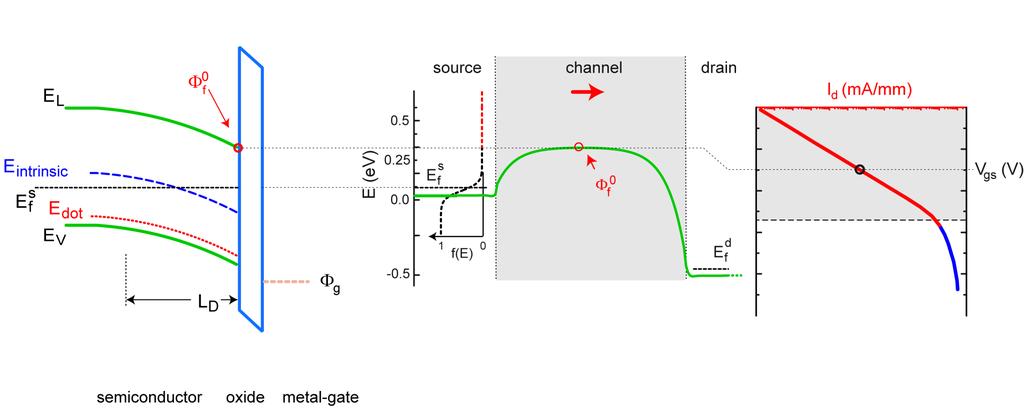
12 Band-to-Band Tunnel FETs gated n-i-p structure ambipolar operation Field-effect modulation of tunneling current minimum leakage determined by size of band gap
13 Band-to-Band Tunnel FETs significantly lower on-state currents exponential increase of I d V ds Drain-Induced-Barrier-Thinning inverse subthreshold slope <60mV/dec only in small gate voltage range avergage slope > 60mV/dec
14 Band-to-Band Tunnel FETs Operational Principles current through TFET can be approximated with Landauer expression How to calculate?
15 Band-to-Band Tunnel FETs Operational Principles approximation of exact bands with triangular potentail barrier energy-independent transmission probability calculated with WKB approximation λ dop is the depletion length in the source contact λ ch is the length scale for potential variations in the channel J. Knoch and J. Appenzeller, DRC
16 Band-to-Band Tunnel FETs Operational Principles

17 Band-to-Band Tunnel FETs Operational Principles exponential screening of potential variations best device layout: wrap-gate architecture with thin nanowire with ultrathin
18 Band-to-Band Tunnel FETs Operational Principles
19 Band-to-Band Tunnel FETs Operational Principles getting rid of f(e) getting rid of k B T
20 Band-to-Band Tunnel FETs Operational Principles exponential increase of I d since thinning of tunneling barrier is dominant
21 Band-to-Band Tunnel FETs Operational Principles point slope exponential increase of I d since thinning of tunneling barrier is dominant average slope
22 Band-to-Band Tunnel FETs Operational Principles band-pass filter behavior effective cooling of f(e) J. Knoch, S. Mantl and J. Appenzeller, Solid-State Electron., 51, 572 (2007).
23 Band-to-Band Tunnel FETs Operational Principles band-pass filter behavior effective cooling of f(e) J. Knoch, S. Mantl and J. Appenzeller, Solid-State Electron., 51, 572 (2007).
24 Tunnel-FET Optimization Device Geometry source-channel p-n- junction as steep as possible small effective mass small (but not too small) band gap
.")
25 Tunnel-FET Optimization Device Geometry back-gate top-gate large parasitic resistance on-current limited by gate leakage M.T. Björk, J. Knoch, H. Schmid, H. Riel, W. Riess, Appl. Phys. Lett., 92, (2008).


26 Tunnel-FET Optimization Device Geometry increased on-current for smaller d ox C. Sandow, J. Knoch, C. Urban, Q.T. Zhao and S. Mantl, Solid-State Electron., 53, 1126 (2009).


27 Tunnel-FET Optimization Device Geometry J. Appenzeller, Y.-M. Lin, J. Knoch, Z. Chen and Ph. Avouris, IEEE Trans. Electron Dev., 52, 2568 (2005).
28 Tunnel-FET Optimization Injecting Conctact source-channel p-n- junction as steep as possible small effective mass small (but not too small) band gap
29 Tunnel-FET Optimization Injecting Conctact
30 Tunnel-FET Optimization Injecting Conctact need low doping concentration and good screening simultaneously J. Appenzeller, J. Knoch, M.T. Bjoerk, H, Schmid, H. Riel and W. Riess, IEEE Trans. Electron Dev., 55, 2827 (2008).
31 Band-to-Band Tunnel FETs significantly lower on-state currents exponential increase of I d V ds Drain-Induced-Barrier-Thinning inverse subthreshold slope <60mV/dec only in small gate voltage range avergage slope > 60mV/dec
32 Drain-Induced Barrier Thinning experiment simulation J. Knoch and J. Appenzeller, phys. stat. sol. a, 205, 679 (2008). C. Sandow, J. Knoch, C. Urban, Q.T. Zhao and S. Mantl, Solid-State Electron., 53, 1126 (2009).
33 Drain-Induced Barrier Thinning inverter transfer curve V in V out sufficient noise margin important for functionality of inverter In Out
34 Drain-Induced Barrier Thinning sufficient noise margin necessary for signal restoration, noise suppression pulse edge sharpening
35 Drain-Induced Barrier Thinning non-linearity of output characteristics of tunnel FETs diminishes noise margin substantially simualtion of tunnel FET inverter

36 Drain-Induced Barrier Thinning injection of charge into channel from drain strong dependence of charge density on drain voltage
37 Drain-Induced Barrier Thinning injection of charge into channel from drain strong dependence of charge density on drain voltage significant Drain-induced barrier thinning but this is no short channel effect
38 Drain-Induced Barrier Thinning semi-analytical, self-consistent calculation based on: increasing E f s helps to get more linear output characteristics but: large E f s yield S 60mV/dec
39 Drain-Induced Barrier Thinning increasing E f s helps to get more linear output characteristics but: large E f s yield S 60mV/dec
. J. Knoch, M.T. Björk, H. Schmid, H. Riel, W. Riess, Device. Research.")
40 Drain-Induced Barrier Thinning in quantum capacitance limit (QCL): QCL attainable in 1D nanowire FETs with wrap-gate structure J. Knoch and J. Appenzeller, phys. stat. sol. a, 205, 679 (2008). J. Knoch, M.T. Björk, H. Schmid, H. Riel, W. Riess, Device. Research. Conf
. J. Knoch, M.T. Björk, H. Schmid, H. Riel, W. Riess, Device. Research. Conf. 2008.")
41 Drain-Induced Barrier Thinning L=50nm d ox = 10nm d ch = 1nm m * = 0.02m 0 L=20nm d ox = 1nm d ch = 1nm m * = 0.1m 0 J. Knoch and J. Appenzeller, phys. stat. sol. a, 205, 679 (2008). J. Knoch, M.T. Björk, H. Schmid, H. Riel, W. Riess, Device. Research. Conf

42 Short Channel Effects conventional FET: drain-induced-barrier-lowering tunnel FET: drain-induced-barrier-thinning

43 Short Channel Effects
44 Short Channel Effects drain-induced barrier thinning J. Appenzeller, J. Knoch, M.T. Björk, H. Schmid, H. Riel W. Riess, IEEE Trans. Electron Dev., 55, 2827 (2008).

45 Short Channel Effects reduced gate impact J. Appenzeller, J. Knoch, M.T. Björk, H. Schmid, H. Riel W. Riess, IEEE Trans. Electron Dev., 55, 2827 (2008).
Comparative Study of Silicon and Germanium Doping-less Tunnel Field Effect Transistors
 IJSTE - International Journal of Science Technology & Engineering Volume 2 Issue 5 November 2015 ISSN (online): 2349-784X Comparative Study of Silicon and Germanium Doping-less Tunnel Field Effect Transistors
Experimentally reported sub-60mv/dec
 Experimentally reported sub-60mv/dec swing in Tunnel FETs? 1 We considered InAs conventional, lateral transistor architectures: GAA nanowire, Fin FETs FETs (Tri gate) UTB,DG SOI Analysis is not directly
Design of Gate-All-Around Tunnel FET for RF Performance
 Drain Current (µa/µm) International Journal of Computer Applications (97 8887) International Conference on Innovations In Intelligent Instrumentation, Optimization And Signal Processing ICIIIOSP-213 Design
Tunneling Field Effect Transistors for Low Power ULSI
 Tunneling Field Effect Transistors for Low Power ULSI Byung-Gook Park Inter-university Semiconductor Research Center and School of Electrical and Computer Engineering Seoul National University Outline
Sub-Threshold Region Behavior of Long Channel MOSFET
 Sub-threshold Region - So far, we have discussed the MOSFET behavior in linear region and saturation region - Sub-threshold region is refer to region where Vt is less than Vt - Sub-threshold region reflects
Performance Evaluation of MISISFET- TCAD Simulation
 Performance Evaluation of MISISFET- TCAD Simulation Tarun Chaudhary Gargi Khanna Rajeevan Chandel ABSTRACT A novel device n-misisfet with a dielectric stack instead of the single insulator of n-mosfet
MODELLING AND IMPLEMENTATION OF SUBTHRESHOLD CURRENTS IN SCHOTTKY BARRIER CNTFETs FOR DIGITAL APPLICATIONS
 www.arpapress.com/volumes/vol11issue3/ijrras_11_3_03.pdf MODELLING AND IMPLEMENTATION OF SUBTHRESHOLD CURRENTS IN SCHOTTKY BARRIER CNTFETs FOR DIGITAL APPLICATIONS Roberto Marani & Anna Gina Perri Electrical
Fin-Shaped Field Effect Transistor (FinFET) Min Ku Kim 03/07/2018
 Min Ku Kim 03/07/2018") Fin-Shaped Field Effect Transistor (FinFET) Min Ku Kim 03/07/2018 ECE 658 Sp 2018 Semiconductor Materials and Device Characterizations OUTLINE Background FinFET Future Roadmap Keeping up w/ Moore s Law
Fin-Shaped Field Effect Transistor (FinFET) Min Ku Kim 03/07/2018 ECE 658 Sp 2018 Semiconductor Materials and Device Characterizations OUTLINE Background FinFET Future Roadmap Keeping up w/ Moore s Law
Session 10: Solid State Physics MOSFET
 Session 10: Solid State Physics MOSFET 1 Outline A B C D E F G H I J 2 MOSCap MOSFET Metal-Oxide-Semiconductor Field-Effect Transistor: Al (metal) SiO2 (oxide) High k ~0.1 ~5 A SiO2 A n+ n+ p-type Si (bulk)
Modeling the Influence of Dielectric Interface Traps on I-V Characteristics of TFETs
 Modeling the Influence of Dielectric Interface Traps on I-V Characteristics of TFETs Jie Min 1, Peter Asbeck UCSD 1 Present address: Global Foundries, Santa Clara, CA Schematic TFET Structures Based on
Leakage Modeling for Devices with Steep Sub-threshold Slope Considering Random Threshold Variations
 Leakage Modeling for Devices with Steep Sub-threshold Slope Considering Random Threshold Variations Ayan Paul, Chaitanya Kshirsagar, Sachin S. Sapatnekar, Steven Koester and Chris H. Kim Electrical and
Transport properties of graphene nanoribbon-based tunnel
 Transport properties of graphene nanoribbon-based tunnel Mark Cheung School of Engineering and Applied Science, Department of Electrical and Computer Engineering Keywords: Monolithic Graphene, Low-Power,
Vertical Nanowire Gate-All-Around p-type Tunneling Field-Effect Transistor With Si 0.8 Ge 0.2 /Si Heterojunction
 2012 International Conference on Solid-State and Integrated Circuit (ICSIC 2012) IPCSIT vol. 32 (2012) (2012) IACSIT Press, Singapore Vertical Nanowire Gate-All-Around p-type Tunneling Field-Effect Transistor
Dependence of Carbon Nanotube Field Effect Transistors Performance on Doping Level of Channel at Different Diameters: on/off current ratio
 Copyright (2012) American Institute of Physics. This article may be downloaded for personal use only. Any other use requires prior permission of the author and the American Institute of Physics. The following
Parameter Optimization Of GAA Nano Wire FET Using Taguchi Method
 Parameter Optimization Of GAA Nano Wire FET Using Taguchi Method S.P. Venu Madhava Rao E.V.L.N Rangacharyulu K.Lal Kishore Professor, SNIST Professor, PSMCET Registrar, JNTUH Abstract As the process technology
III-V CMOS: Quo Vadis?
 III-V CMOS: Quo Vadis? J. A. del Alamo, X. Cai, W. Lu, A. Vardi, and X. Zhao Microsystems Technology Laboratories Massachusetts Institute of Technology Compound Semiconductor Week 2018 Cambridge, MA, May
CARBON nanotubes (CN) have been identified as an
 have been identified as an") 2568 IEEE TRANSACTIONS ON ELECTRON DEVICES, VOL. 52, NO. 12, DECEMBER 2005 Comparing Carbon Nanotube Transistors The Ideal Choice: A Novel Tunneling Device Design Joerg Appenzeller, Senior Member, IEEE,
2568 IEEE TRANSACTIONS ON ELECTRON DEVICES, VOL. 52, NO. 12, DECEMBER 2005 Comparing Carbon Nanotube Transistors The Ideal Choice: A Novel Tunneling Device Design Joerg Appenzeller, Senior Member, IEEE,
Alternative Channel Materials for MOSFET Scaling Below 10nm
 Alternative Channel Materials for MOSFET Scaling Below 10nm Doug Barlage Electrical Requirements of Channel Mark Johnson Challenges With Material Synthesis Introduction Outline Challenges with scaling
UNIVERSITY OF CALIFORNIA AT BERKELEY College of Engineering Department of Electrical Engineering and Computer Sciences.
 UNIVERSITY OF CALIFORNIA AT BERKELEY College of Engineering Department of Electrical Engineering and Computer Sciences Discussion #9 EE 05 Spring 2008 Prof. u MOSFETs The standard MOSFET structure is shown
FUNDAMENTALS OF MODERN VLSI DEVICES
 19-13- FUNDAMENTALS OF MODERN VLSI DEVICES YUAN TAUR TAK H. MING CAMBRIDGE UNIVERSITY PRESS Physical Constants and Unit Conversions List of Symbols Preface page xi xiii xxi 1 INTRODUCTION I 1.1 Evolution
Lecture 31 - The Short Metal-Oxide-Semiconductor Field-Effect Transistor (cont.) April 25, 2007
 April 25, 2007") 6.720J/3.43J - Integrated Microelectronic Devices - Spring 2007 Lecture 31-1 Lecture 31 - The Short Metal-Oxide-Semiconductor Field-Effect Transistor (cont.) April 25, 2007 Contents: 1. Short-channel effects
6.720J/3.43J - Integrated Microelectronic Devices - Spring 2007 Lecture 31-1 Lecture 31 - The Short Metal-Oxide-Semiconductor Field-Effect Transistor (cont.) April 25, 2007 Contents: 1. Short-channel effects
Band-Offset Engineering for GeSn-SiGeSn Hetero Tunnel FETs and the Role of Strain
 Received 2 September 2014; revised 5 January 2015; accepted 8 January 2015. Date of current version 22 April 2015. The review of this paper was arranged by Editor A. C. Seabaugh. Digital Object Identifier
Atomic-layer deposition of ultrathin gate dielectrics and Si new functional devices
 Atomic-layer deposition of ultrathin gate dielectrics and Si new functional devices Anri Nakajima Research Center for Nanodevices and Systems, Hiroshima University 1-4-2 Kagamiyama, Higashi-Hiroshima,
IEEE TRANSACTIONS ON ELECTRON DEVICES 1
 IEEE TRANSACTIONS ON ELECTRON DEVICES 1 Current and Noise Properties of InAs Nanowire Transistors With Asymmetric Contacts Induced by Gate Overlap Collin J. Delker, Member, IEEE, Yunlong Zi, Chen Yang,
INTERNATIONAL JOURNAL OF APPLIED ENGINEERING RESEARCH, DINDIGUL Volume 1, No 3, 2010
 Low Power CMOS Inverter design at different Technologies Vijay Kumar Sharma 1, Surender Soni 2 1 Department of Electronics & Communication, College of Engineering, Teerthanker Mahaveer University, Moradabad
Fabrication and Characterization of Pseudo-MOSFETs
 Fabrication and Characterization of Pseudo-MOSFETs March 19, 2014 Contents 1 Introduction 2 2 The pseudo-mosfet 3 3 Device Fabrication 5 4 Electrical Measurement and Characterization 7 5 Writing your Report
Reconfigurable Si-Nanowire Devices
 Reconfigurable Si-Nanowire Devices André Heinzig, Walter M. Weber, Dominik Martin, Jens Trommer, Markus König and Thomas Mikolajick andre.heinzig@namlab.com log I d Present CMOS technology ~ 88 % of IC
Alternatives to standard MOSFETs. What problems are we really trying to solve?
 Alternatives to standard MOSFETs A number of alternative FET schemes have been proposed, with an eye toward scaling up to the 10 nm node. Modifications to the standard MOSFET include: Silicon-in-insulator
Investigation of Feasibility of Tunneling Field Effect Transistor (TFET) as Highly Sensitive and Multi-sensing Biosensors
 as Highly Sensitive and Multi-sensing Biosensors") JOURNAL OF SEMICONDUCTOR TECHNOLOGY AND SCIENCE, VOL.17, NO.1, FEBRUARY, 2017 ISSN(Print) 1598-1657 https://doi.org/10.5573/jsts.2017.17.1.141 ISSN(Online) 2233-4866 Investigation of Feasibility of Tunneling
JOURNAL OF SEMICONDUCTOR TECHNOLOGY AND SCIENCE, VOL.17, NO.1, FEBRUARY, 2017 ISSN(Print) 1598-1657 https://doi.org/10.5573/jsts.2017.17.1.141 ISSN(Online) 2233-4866 Investigation of Feasibility of Tunneling
Three Terminal Devices
 Three Terminal Devices - field effect transistor (FET) - bipolar junction transistor (BJT) - foundation on which modern electronics is built - active devices - devices described completely by considering
SCHOTTKY-BARRIER metal oxide semiconductor fieldeffect
 IEEE TRANSACTIONS ON ELECTRON DEVICES, VOL. 58, NO. 2, FEBRUARY 2011 427 Analysis of Transconductance (g m ) in Schottky-Barrier MOSFETs Sung-Jin Choi, Chel-Jong Choi, Jee-Yeon Kim, Moongyu Jang, and Yang-Kyu
Beyond Transistor Scaling: New Devices for Ultra Low Energy Information Processing
 Beyond Transistor Scaling: New Devices for Ultra Low Energy Information Processing Prof. Tsu Jae King Liu Department of Electrical Engineering and Computer Sciences University of California, Berkeley,
DG-FINFET LOGIC DESIGN USING 32NM TECHNOLOGY
 International Journal of Knowledge Management & e-learning Volume 3 Number 1 January-June 2011 pp. 1-5 DG-FINFET LOGIC DESIGN USING 32NM TECHNOLOGY K. Nagarjuna Reddy 1, K. V. Ramanaiah 2 & K. Sudheer
Study of Pattern Area of Logic Circuit. with Tunneling Field-Effect Transistors
 Contemporary Engineering Sciences, Vol. 6, 2013, no. 6, 273-284 HIKARI Ltd, www.m-hikari.com http://dx.doi.org/10.12988/ces.2013.3632 Study of Pattern Area of Logic Circuit with Tunneling Field-Effect
MOSFET short channel effects
 MOSFET short channel effects overview Five different short channel effects can be distinguished: velocity saturation drain induced barrier lowering (DIBL) impact ionization surface scattering hot electrons
Optimization of Double Gate Vertical Channel Tunneling Field Effect Transistor (DVTFET) with Dielectric Sidewall
 with Dielectric Sidewall") JOURNAL OF SEMICONDUCTOR TECHNOLOGY AND SCIENCE, VOL.17, NO.2, APRIL, 2017 ISSN(Print) 1598-1657 https://doi.org/10.5573/jsts.2017.17.2.192 ISSN(Online) 2233-4866 Optimization of Double Gate Vertical Channel
JOURNAL OF SEMICONDUCTOR TECHNOLOGY AND SCIENCE, VOL.17, NO.2, APRIL, 2017 ISSN(Print) 1598-1657 https://doi.org/10.5573/jsts.2017.17.2.192 ISSN(Online) 2233-4866 Optimization of Double Gate Vertical Channel
Analytical Model for Surface Potential and Inversion Charge of Dual Material Double Gate Son MOSFET
 International Journal of Engineering and Technical Research (IJETR) Analytical Model for Surface Potential and Inversion Charge of Dual Material Double Gate Son MOSFET Gaurabh Yadav, Mr. Vaibhav Purwar
Record I on (0.50 ma/μm at V DD = 0.5 V and I off = 100 na/μm) 25 nm-gate-length ZrO 2 /InAs/InAlAs MOSFETs
 25 nm-gate-length ZrO 2 /InAs/InAlAs MOSFETs") Record I on (0.50 ma/μm at V DD = 0.5 V and I off = 100 na/μm) 25 nm-gate-length ZrO 2 /InAs/InAlAs MOSFETs Sanghoon Lee 1*, V. Chobpattana 2,C.-Y. Huang 1, B. J. Thibeault 1, W. Mitchell 1, S. Stemmer
Record I on (0.50 ma/μm at V DD = 0.5 V and I off = 100 na/μm) 25 nm-gate-length ZrO 2 /InAs/InAlAs MOSFETs Sanghoon Lee 1*, V. Chobpattana 2,C.-Y. Huang 1, B. J. Thibeault 1, W. Mitchell 1, S. Stemmer
Drive performance of an asymmetric MOSFET structure: the peak device
 MEJ 499 Microelectronics Journal Microelectronics Journal 30 (1999) 229 233 Drive performance of an asymmetric MOSFET structure: the peak device M. Stockinger a, *, A. Wild b, S. Selberherr c a Institute
NAME: Last First Signature
 UNIVERSITY OF CALIFORNIA, BERKELEY College of Engineering Department of Electrical Engineering and Computer Sciences EE 130: IC Devices Spring 2003 FINAL EXAMINATION NAME: Last First Signature STUDENT
NW-NEMFET: Steep Subthreshold Nanowire Nanoelectromechanical Field-Effect Transistor
 NW-NEMFET: Steep Subthreshold Nanowire Nanoelectromechanical Field-Effect Transistor Jie Xiang Electrical and Computer Engineering and Materials Science Engineering University of California, San Diego
SIMULATION STUDY OF BALLISTIC CARBON NANOTUBE FIELD EFFECT TRANSISTOR
 SIMULATION STUDY OF BALLISTIC CARBON NANOTUBE FIELD EFFECT TRANSISTOR RAHMAT SANUDIN IEEE NATIONAL SYMPOSIUM ON MICROELECTRONICS 2005 21-24 NOVEMBER 2005 KUCHING SARAWAK Simulation Study of Ballistic Carbon
Design of Tunnel FET and its Performance characteristics with various materials
 Design of Tunnel FET and its Performance characteristics with various materials 1 G.SANKARAIAH, 2 CH.SATHYANARAYANA 1 PG Student Sreenidhi Institute of Science and Technology, 2 Assistant Professor 1,
ECE520 VLSI Design. Lecture 2: Basic MOS Physics. Payman Zarkesh-Ha
 ECE520 VLSI Design Lecture 2: Basic MOS Physics Payman Zarkesh-Ha Office: ECE Bldg. 230B Office hours: Wednesday 2:00-3:00PM or by appointment E-mail: pzarkesh@unm.edu Slide: 1 Review of Last Lecture Semiconductor
Integration of III-V heterostructure tunnel FETs on Si using Template Assisted Selective Epitaxy (TASE)
") Integration of III-V heterostructure tunnel FETs on Si using Template Assisted Selective Epitaxy (TASE) K. Moselund 1, D. Cutaia 1. M. Borg 1, H. Schmid 1, S. Sant 2, A. Schenk 2 and H. Riel 1 1 IBM Research
Integration of III-V heterostructure tunnel FETs on Si using Template Assisted Selective Epitaxy (TASE) K. Moselund 1, D. Cutaia 1. M. Borg 1, H. Schmid 1, S. Sant 2, A. Schenk 2 and H. Riel 1 1 IBM Research
Saving Moore s Law Down To 1nm Channels With Anisotropic Effective Mass
 Saving Moore s Law Down To 1nm Channels With Anisotropic Effective Mass arxiv:1605.03979v1 [cond-mat.mes-hall] 12 May 2016 Hesameddin Ilatikhameneh 1*, Tarek Ameen 1*, Bozidar Novakovic 1, Yaohua Tan 1,
Silicon Nanowire Tunneling Field-Effect Transistor Arrays: Improving Subthreshold Performance Using Excimer Laser Annealing
 Purdue University Purdue e-pubs Birck and NCN Publications Birck Nanotechnology Center 6-21-2011 Silicon Nanowire Tunneling Field-Effect Transistor Arrays: Improving Subthreshold Performance Using Excimer
Digital Electronics. By: FARHAD FARADJI, Ph.D. Assistant Professor, Electrical and Computer Engineering, K. N. Toosi University of Technology
 K. N. Toosi University of Technology Chapter 7. Field-Effect Transistors By: FARHAD FARADJI, Ph.D. Assistant Professor, Electrical and Computer Engineering, K. N. Toosi University of Technology http://wp.kntu.ac.ir/faradji/digitalelectronics.htm
Characterization of Variable Gate Oxide Thickness MOSFET with Non-Uniform Oxide Thicknesses for Sub-Threshold Leakage Current Reduction
 2012 International Conference on Solid-State and Integrated Circuit (ICSIC 2012) IPCSIT vol. 32 (2012) (2012) IACSIT Press, Singapore Characterization of Variable Gate Oxide Thickness MOSFET with Non-Uniform
Optimization of Direct Tunneling Gate Leakage Current in Ultrathin Gate Oxide FET with High-K Dielectrics
 Optimization of Direct Tunneling Gate Leakage Current in Ultrathin Gate Oxide FET with High-K Dielectrics Sweta Chander 1, Pragati Singh 2, S Baishya 3 1,2,3 Department of Electronics & Communication Engineering,
EECS130 Integrated Circuit Devices
 EECS130 Integrated Circuit Devices Professor Ali Javey 11/6/2007 MOSFETs Lecture 6 BJTs- Lecture 1 Reading Assignment: Chapter 10 More Scalable Device Structures Vertical Scaling is important. For example,
Design and Analysis of High Frequency InN Tunnel Transistors
 Design and Analysis of High Frequency InN Tunnel Transistors Krishnendu Ghosh and Uttam Singisetti Department of Electrical Engineering, University at Buffalo, The State University of New York, Buffalo,
Solid State Devices- Part- II. Module- IV
 Solid State Devices- Part- II Module- IV MOS Capacitor Two terminal MOS device MOS = Metal- Oxide- Semiconductor MOS capacitor - the heart of the MOSFET The MOS capacitor is used to induce charge at the
FET. Field Effect Transistors ELEKTRONIKA KONTROL. Eka Maulana, ST, MT, M.Eng. Universitas Brawijaya. p + S n n-channel. Gate. Basic structure.
 FET Field Effect Transistors ELEKTRONIKA KONTROL Basic structure Gate G Source S n n-channel Cross section p + p + p + G Depletion region Drain D Eka Maulana, ST, MT, M.Eng. Universitas Brawijaya S Channel
Nanoscale III-V CMOS
 Nanoscale III-V CMOS J. A. del Alamo Microsystems Technology Laboratories Massachusetts Institute of Technology SEMI Advanced Semiconductor Manufacturing Conference Saratoga Springs, NY; May 16-19, 2016
INTRODUCTION TO MOS TECHNOLOGY
 INTRODUCTION TO MOS TECHNOLOGY 1. The MOS transistor The most basic element in the design of a large scale integrated circuit is the transistor. For the processes we will discuss, the type of transistor
Power MOSFET Zheng Yang (ERF 3017,
 ECE442 Power Semiconductor Devices and Integrated Circuits Power MOSFET Zheng Yang (ERF 3017, email: yangzhen@uic.edu) Evolution of low-voltage (
Fundamental Tradeoff between Conductance and Subthreshold Swing Voltage for Barrier Thickness Modulation in Tunnel Field Effect Transistors
 Fundamental Tradeoff between Conductance and Subthreshold Swing Voltage for Barrier Thickness Modulation in Tunnel Field Effect Transistors Sapan Agarwal Eli Yablonovitch Electrical Engineering and Computer
EE301 Electronics I , Fall
 EE301 Electronics I 2018-2019, Fall 1. Introduction to Microelectronics (1 Week/3 Hrs.) Introduction, Historical Background, Basic Consepts 2. Rewiev of Semiconductors (1 Week/3 Hrs.) Semiconductor materials
Why Scaling? CPU speed Chip size R, C CPU can increase speed by reducing occupying area.
 Why Scaling? Higher density : Integration of more transistors onto a smaller chip : reducing the occupying area and production cost Higher Performance : Higher current drive : smaller metal to metal capacitance
Performance Comparison of CMOS and Finfet Based Circuits At 45nm Technology Using SPICE
 RESEARCH ARTICLE OPEN ACCESS Performance Comparison of CMOS and Finfet Based Circuits At 45nm Technology Using SPICE Mugdha Sathe*, Dr. Nisha Sarwade** *(Department of Electrical Engineering, VJTI, Mumbai-19)
EFFECT OF THRESHOLD VOLTAGE AND CHANNEL LENGTH ON DRAIN CURRENT OF SILICON N-MOSFET
 EFFECT OF THRESHOLD VOLTAGE AND CHANNEL LENGTH ON DRAIN CURRENT OF SILICON N-MOSFET A.S.M. Bakibillah Nazibur Rahman Dept. of Electrical & Electronic Engineering, American International University Bangladesh
III-V Vertical Nanowire FETs with Steep Subthreshold Towards Sub-10 nm Diameter Devices
 III-V Vertical Nanowire FETs with Steep Subthreshold Towards Sub-10 nm Diameter Devices Jesús A. del Alamo, Xin Zhao, Wenjie Lu, Alon Vardi Microsystems Technology Laboratories, MIT E 3 S Retreat September
Analog Performance of Scaled Bulk and SOI MOSFETs
 Analog Performance of Scaled and SOI MOSFETs Sushant S. Suryagandh, Mayank Garg, M. Gupta, Jason C.S. Woo Department. of Electrical Engineering University of California, Los Angeles CA 99, USA. woo@icsl.ucla.edu
Simulation and Analysis of CNTFETs based Logic Gates in HSPICE
 Simulation and Analysis of CNTFETs based Logic Gates in HSPICE Neetu Sardana, 2 L.K. Ragha M.E Student, 2 Guide Electronics Department, Terna Engineering College, Navi Mumbai, India Abstract Conventional
MOS Capacitance and Introduction to MOSFETs
 ECE-305: Fall 2016 MOS Capacitance and Introduction to MOSFETs Professor Peter Bermel Electrical and Computer Engineering Purdue University, West Lafayette, IN USA pbermel@purdue.edu 11/4/2016 Pierret,
CHAPTER 2 LITERATURE REVIEW
 CHAPTER 2 LITERATURE REVIEW 2.1 Introduction of MOSFET The structure of the MOS field-effect transistor (MOSFET) has two regions of doping opposite that of the substrate, one at each edge of the MOS structure
Lecture-45. MOS Field-Effect-Transistors Threshold voltage
 Lecture-45 MOS Field-Effect-Transistors 7.4. Threshold voltage In this section we summarize the calculation of the threshold voltage and discuss the dependence of the threshold voltage on the bias applied
Reliability of deep submicron MOSFETs
 Invited paper Reliability of deep submicron MOSFETs Francis Balestra Abstract In this work, a review of the reliability of n- and p-channel Si and SOI MOSFETs as a function of gate length and temperature
Ambipolar electronics
 Ambipolar electronics Xuebei Yang and Kartik Mohanram Department of Electrical and Computer Engineering, Rice University, Houston {xy3,mr11,kmram}@rice.edu Rice University Technical Report TREE12 March
Supporting Information
 Supporting Information Fabrication and Transfer of Flexible Few-Layers MoS 2 Thin Film Transistors to any arbitrary substrate Giovanni A. Salvatore 1, *, Niko Münzenrieder 1, Clément Barraud 2, Luisa Petti
Floating Body and Hot Carrier Effects in Ultra-Thin Film SOI MOSFETs
 Floating Body and Hot Carrier Effects in Ultra-Thin Film SOI MOSFETs S.-H. Renn, C. Raynaud, F. Balestra To cite this version: S.-H. Renn, C. Raynaud, F. Balestra. Floating Body and Hot Carrier Effects
 NTFET LH m.hejazifar@srbiau.ac.ir sedigh@iaurasht.ac.ir : N I on < 5 ownloaded from jiaeee.com at 15:42 +0330 on Thursday ecember 6th 2018 LS 1 2 MOS LH- NTFET MOSFET N 1nm 15nm HfO2 2nm 2 15 nm 30nm 0/2
Lecture - 18 Transistors
 Electronic Materials, Devices and Fabrication Dr. S. Prarasuraman Department of Metallurgical and Materials Engineering Indian Institute of Technology, Madras Lecture - 18 Transistors Last couple of classes
Design of 45 nm Fully Depleted Double Gate SOI MOSFET
 Design of 45 nm Fully Depleted Double Gate SOI MOSFET 1. Mini Bhartia, 2. Shrutika. Satyanarayana, 3. Arun Kumar Chatterjee 1,2,3. Thapar University, Patiala Abstract Advanced MOSFETS such as Fully Depleted
Novel Electrostatically Doped Planar Field-Effect Transistor for High Temperature Applications. Tillmann Krauss, Frank Wessely and Udo Schwalke
 Novel Electrostatically Doped Planar Field-Effect Transistor for High Temperature Applications Tillmann Krauss, Frank Wessely and Udo Schwalke Institute for Semiconductor Technology and Nanoelectronics,
ECE 340 Lecture 40 : MOSFET I
 ECE 340 Lecture 40 : MOSFET I Class Outline: MOS Capacitance-Voltage Analysis MOSFET - Output Characteristics MOSFET - Transfer Characteristics Things you should know when you leave Key Questions How do
Semiconductor Memory: DRAM and SRAM. Department of Electrical and Computer Engineering, National University of Singapore
 Semiconductor Memory: DRAM and SRAM Outline Introduction Random Access Memory (RAM) DRAM SRAM Non-volatile memory UV EPROM EEPROM Flash memory SONOS memory QD memory Introduction Slow memories Magnetic
Semiconductor Physics and Devices
 Metal-Semiconductor and Semiconductor Heterojunctions The Metal-Oxide-Semiconductor Field-Effect Transistor (MOSFET) is one of two major types of transistors. The MOSFET is used in digital circuit, because
DESIGN OF 20 nm FinFET STRUCTURE WITH ROUND FIN CORNERS USING SIDE SURFACE SLOPE VARIATION
 Journal of Electron Devices, Vol. 18, 2013, pp. 1537-1542 JED [ISSN: 1682-3427 ] DESIGN OF 20 nm FinFET STRUCTURE WITH ROUND FIN CORNERS USING SIDE SURFACE SLOPE VARIATION Suman Lata Tripathi and R. A.
A New Self-aligned Quantum-Well MOSFET Architecture Fabricated by a Scalable Tight-Pitch Process
 A New Self-aligned Quantum-Well MOSFET Architecture Fabricated by a Scalable Tight-Pitch Process Jianqiang Lin, Xin Zhao, Tao Yu, Dimitri A. Antoniadis, and Jesús A. del Alamo Microsystems Technology Laboratories,
General look back at MESFET processing. General principles of heterostructure use in FETs
 SMA5111 - Compound Semiconductors Lecture 11 - Heterojunction FETs - General HJFETs, HFETs Last items from Lec. 10 Depletion mode vs enhancement mode logic Complementary FET logic (none exists, or is likely
M. Jagadesh Kumar and G. Venkateshwar Reddy Department of Electrical Engineering, Indian Institute of Technology, Hauz Khas, New Delhi , India
 M. Jagadesh Kumar and G. V. Reddy, "Diminished Short Channel Effects in Nanoscale Double- Gate Silicon-on-Insulator Metal Oxide Field Effect Transistors due to Induced Back-Gate Step Potential," Japanese
Design cycle for MEMS
 Design cycle for MEMS Design cycle for ICs IC Process Selection nmos CMOS BiCMOS ECL for logic for I/O and driver circuit for critical high speed parts of the system The Real Estate of a Wafer MOS Transistor
MSE 410/ECE 340: Electrical Properties of Materials Fall 2016 Micron School of Materials Science and Engineering Boise State University
 MSE 410/ECE 340: Electrical Properties of Materials Fall 2016 Micron School of Materials Science and Engineering Boise State University Practice Final Exam 1 Read the questions carefully Label all figures
Modeling & Analysis of Surface Potential and Threshold Voltage for Narrow channel 3D FDSOI MOSFET
 Modeling & Analysis of Surface Potential and Threshold Voltage for Narrow channel 3D... 273 IJCTA, 9(22), 2016, pp. 273-278 International Science Press Modeling & Analysis of Surface Potential and Threshold
Solid State Device Fundamentals
 Solid State Device Fundamentals 4.4. Field Effect Transistor (MOSFET) ENS 463 Lecture Course by Alexander M. Zaitsev alexander.zaitsev@csi.cuny.edu Tel: 718 982 2812 4N101b 1 Field-effect transistor (FET)
Active Pixel Sensors Fabricated in a Standard 0.18 um CMOS Technology
 Active Pixel Sensors Fabricated in a Standard.18 um CMOS Technology Hui Tian, Xinqiao Liu, SukHwan Lim, Stuart Kleinfelder, and Abbas El Gamal Information Systems Laboratory, Stanford University Stanford,
Semiconductor TCAD Tools
 Device Design Consideration for Nanoscale MOSFET Using Semiconductor TCAD Tools Teoh Chin Hong and Razali Ismail Department of Microelectronics and Computer Engineering, Universiti Teknologi Malaysia,
EE241 - Spring 2013 Advanced Digital Integrated Circuits. Projects. Groups of 3 Proposals in two weeks (2/20) Topics: Lecture 5: Transistor Models
 Topics: Lecture 5: Transistor Models") EE241 - Spring 2013 Advanced Digital Integrated Circuits Lecture 5: Transistor Models Projects Groups of 3 Proposals in two weeks (2/20) Topics: Soft errors in datapaths Soft errors in memory Integration
EE241 - Spring 2013 Advanced Digital Integrated Circuits Lecture 5: Transistor Models Projects Groups of 3 Proposals in two weeks (2/20) Topics: Soft errors in datapaths Soft errors in memory Integration
Lecture #29. Moore s Law
 Lecture #29 ANNOUNCEMENTS HW#15 will be for extra credit Quiz #6 (Thursday 5/8) will include MOSFET C-V No late Projects will be accepted after Thursday 5/8 The last Coffee Hour will be held this Thursday
Logic circuits based on carbon nanotubes
 Available online at www.sciencedirect.com Physica E 16 (23) 42 46 www.elsevier.com/locate/physe Logic circuits based on carbon nanotubes A. Bachtold a;b;, P. Hadley a, T. Nakanishi a, C. Dekker a a Department
Week 9a OUTLINE. MOSFET I D vs. V GS characteristic Circuit models for the MOSFET. Reading. resistive switch model small-signal model
 Week 9a OUTLINE MOSFET I vs. V GS characteristic Circuit models for the MOSFET resistive switch model small-signal model Reading Rabaey et al.: Chapter 3.3.2 Hambley: Chapter 12 (through 12.5); Section
improving further the mobility, and therefore the channel conductivity. The positive pattern definition proposed by Hirayama [6] was much improved in
![improving further the mobility, and therefore the channel conductivity. The positive pattern definition proposed by Hirayama [6] was much improved in](/thumbs/91/107553446.jpg "improving further the mobility, and therefore the channel conductivity. The positive pattern definition proposed by Hirayama [6] was much improved in") The two-dimensional systems embedded in modulation-doped heterostructures are a very interesting and actual research field. The FIB implantation technique can be successfully used to fabricate using these
The two-dimensional systems embedded in modulation-doped heterostructures are a very interesting and actual research field. The FIB implantation technique can be successfully used to fabricate using these
Channel Engineering for Submicron N-Channel MOSFET Based on TCAD Simulation
 Australian Journal of Basic and Applied Sciences, 2(3): 406-411, 2008 ISSN 1991-8178 Channel Engineering for Submicron N-Channel MOSFET Based on TCAD Simulation 1 2 3 R. Muanghlua, N. Vittayakorn and A.
Down-scaling of Thin-Film Transistors: Opportunities and Design Challenges. University, Shanghai , China
 Down-scaling of Thin-Film Transistors: Opportunities and Design Challenges X. Guo a, R. Sporea b, J. M. Shannon b, and S. R. P. Silva b a National Engineering Laboratory for TFT-LCD Technology, Shanghai
IEEE TRANSACTIONS ON ELECTRON DEVICES 1
 IEEE TRANSACTIONS ON ELECTRON DEVICES 1 Low-Frequency Noise Contributions from Channel and Contacts in InAs Nanowire Transistors Collin J. Delker, Member, IEEE, Yunlong Zi, Chen Yang, and David B. Janes,
SCALING AND NUMERICAL SIMULATION ANALYSIS OF 50nm MOSFET INCORPORATING DIELECTRIC POCKET (DP-MOSFET)
") SCALING AND NUMERICAL SIMULATION ANALYSIS OF 50nm MOSFET INCORPORATING DIELECTRIC POCKET (DP-MOSFET) Zul Atfyi Fauzan M. N., Ismail Saad and Razali Ismail Faculty of Electrical Engineering, Universiti
SCALING AND NUMERICAL SIMULATION ANALYSIS OF 50nm MOSFET INCORPORATING DIELECTRIC POCKET (DP-MOSFET) Zul Atfyi Fauzan M. N., Ismail Saad and Razali Ismail Faculty of Electrical Engineering, Universiti
Design and Optimization of Half Subtractor Circuits for Low-Voltage Low-Power Applications
 ABSTRACT Design and Optimization of Half Subtractor Circuits for Low-Voltage Low-Power Applications Abhishek Sharma,Gunakesh Sharma,Shipra ishra.tech. Embedded system & VLSI Design NIT,Gwalior.P. India
FinFET-based Design for Robust Nanoscale SRAM
 FinFET-based Design for Robust Nanoscale SRAM Prof. Tsu-Jae King Liu Dept. of Electrical Engineering and Computer Sciences University of California at Berkeley Acknowledgements Prof. Bora Nikoli Zheng