Power MOSFET Zheng Yang (ERF 3017,
|
|
|
- Norman Peters
- 5 years ago
- Views:
Transcription
1 ECE442 Power Semiconductor Devices and Integrated Circuits Power MOSFET Zheng Yang (ERF 3017,
2 Evolution of low-voltage (<100V) power rectifiers Chapter 5 in textbook; discussed. Chapter 4 in textbook; discussed. Not covered by this textbook; did NOT discuss. Not covered by this textbook; did NOT discuss. (JBS: junction barrier controlled Schottky) (TMBS: trench MOS barrier rectifier Schottky) [cited from B. J. Baliga, Trends in Power Semiconductor Devices, IEEE Transactions on Electronic Devices 43(10), (1996)] 2
3 Evolution of high-voltage (>300V) power rectifiers Chapter 5 in textbook; discussed. (MPS: merged P-i-N and Schottky) Not covered by this textbook; did NOT discuss. Covered by this textbook briefly (Section 4.4.4); discussed very briefly. [cited from B. J. Baliga, Trends in Power Semiconductor Devices, IEEE Transactions on Electronic Devices 43(10), (1996)] 3
4 Evolution of power MOSFET structures Chapter 6 in textbook; will discuss. Chapter 6 in textbook; will discuss. Chapter 6 in textbook; will discuss. Not covered by this textbook; will NOT discuss. [cited from B. J. Baliga, Trends in Power Semiconductor Devices, IEEE Transactions on Electronic Devices 43(10), (1996)] 4
5 Power MOSFET Background The vertical power metal-oxide-semiconductor field effect transistor (MOSFET) structure was developed in the mid-1970s to obtain improved performance when compared with the existing power bipolar transistors. One of the major issues with the power bipolar transistor structure was its low-current gain when designed to support high voltages. In addition, power bipolar transistors could not be operated at high frequencies due to the large storage time related to the injected charge in their drift regions and were prone to destructive failure during hard switching in applications with inductive loads. The replacement of these current-controlled devices with a voltage-controlled device was attractive from an application s viewpoint. The high input impedance of the metal-oxide-semiconductor (MOS)- gate structure simplified the drive circuit requirements when compared with bipolar transistors being used at that time. In addition, their superior switching speed opened new applications operating in the khz frequency domain. Today, power MOSFETs are the most commonly used power switches in applications where the operating voltages are below 200 V. The vertical power MOSFETs were initially considered to be ideal power switches due to their high input impedance and fast switching speed. However, their power-handling capability was constrained by the internal resistance within the structure between the drain and source electrodes. The power dissipated due to the Ohmic voltage drop in the internal resistance limited the current-handling capability of the power MOSFETs as well as the efficiency of the power circuits in which they were utilized. 5
6 MOS Interface Physics Flat Band Conditions
7 MOS Interface Physics Accumulation Conditions
8 MOS Interface Physics Depletion Conditions
9 MOS Interface Physics Inversion Conditions
10 MOS Surface Charge Analysis


11 MOS Surface Charge Analysis (cont d)
12 MOS Surface Charge Analysis (cont d)
13 MOS Surface Charge Analysis (cont d)

14 Maximum Depletion Width
15 Threshold Voltage
16 Threshold Voltage (work function difference)
17 Threshold Voltage (oxide charge) (n-channel)

")
18 Threshold Voltage (oxide charge) (p-channel)
19 MOSFET Channel Resistance
20 MOSFET Channel Resistance (cont d)
21 V-MOSFET (V-groove MOSFET ) The first high-voltage power MOSFET structure was developed by using a V-groove etching process during the 1970s. A cross section of this V-MOSFET structure is illustrated in the left hand side figure. The N+ source and drain regions in the vertical power MOSFET structure are separated by a P-base region, resulting in the formation of two P-N junctions labeled J1 and J2 in the figure. A V-groove is formed at the upper surface that penetrates through both the junctions. The gate electrode is placed inside the V- groove after creating a gate oxide on its surface, preferably by thermal oxidation of the silicon. Without the application of a gate bias, junction J1 becomes reverse biased when a positive bias is applied to the drain electrode. A high voltage can be supported under these conditions by appropriate choice of the doping concentration and thickness of the N-drift region. The second junction J2 is short circuited by overlapping the source electrode over the junction as illustrated in the figure to suppress the parasitic bipolar transistor. With proper design considerations, the breakdown voltage approaches that for a P-N diode. Current flow between the drain and source electrodes of the V-MOSFET structure can be induced by the formation of a channel at the surface of the P-base region below the gate oxide. A positive bias applied to the gate electrode attracts electrons to the semiconductor surface under the gate oxide. These electrons provide a path for current flow between the source and the drain. The maximum current carrying capability is determined by the internal resistance within the structure. A smaller resistance can be achieved by using smaller dimensions in the cell structure to increase the channel density.
22 Challenges of V-MOSFETs The V-MOSFET structure fell out of favor because of manufacturing difficulties. The V- groove was formed by using a potassium hydroxide-based etch for silicon, which exhibits different etch rates for various silicon surface orientations. It was found that the potassium from the etch solutions contaminates the gate oxide, producing instabilities during long-term operation of the V-MOSFET structure. In addition, the sharp corner at the bottom of the V- groove was found to degrade the breakdown voltage.
23 D-MOSFET (or VD-MOSFET) Note: Different books sometimes use different names of this type of power MOSFET. The names VD-MOSFET, vertical-diffused MOSFET, double-diffused MOSFET, and DMOSFET refer to the exactly same device structure.
24 D-MOSFET Structure A cross section of the basic cell structure for the DMOSFET is illustrated in above figure. This device structure is fabricated by starting with an N-type epitaxial layer grown on a heavily doped N+ substrate. The channel is formed by the difference in lateral extension of the P-base and N+ source regions produced by their diffusion cycles. Both regions are self-aligned to the left-hand side and right-hand side of the gate region during ion implantation to introduce the respective dopants. A refractory gate electrode, such as polysilicon, is required to allow diffusion of the dopants under the gate electrode at elevated temperatures.

25 How a D-MOSFET works? Without the application of a gate bias, a high voltage can be supported in the D-MOSFET structure when a positive bias is applied to the drain. In this case, junction J 1 formed between the P-base region and the N-drift region becomes reverse biased. The voltage is supported mainly within the thick lightly doped N-drift region. Drain current flow in the D-MOSFET structure is induced by the application of a positive bias to the gate electrode. This produces an inversion layer at the surface of the P-base region under the gate electrode. This inversion layer channel provides a path for transport of electrons from the source to the drain when a positive drain voltage is applied.

26 How a D-MOSFET works? (cont d) After transport from the source region through the channel, the electrons enter the N-drift region at the upper surface of the device structure. They are then transported through a relatively narrow JFET region located between the adjacent P- base regions within the D-MOSFET structure. The constriction of the current flow through the JFET region substantially increases the internal resistance of the D-MOSFET structure. A careful optimization of the gate width (W G ) is required to minimize the internal resistance for this structure. In addition, it is customary to enhance the doping concentration in the JFET region to reduce the resistance to current flow through this portion of the device structure. After being transported through the JFET region, the electrons enter the N-drift region below junction J 1. The current spreads from the relatively narrow JFET region to the entire width of the cell cross section. This non-uniform current distribution within the drift region increases its resistance, making the internal resistance of the D-MOSFET structure larger than the ideal specific on-resistance of the drift region. The large internal resistance for the D-MOSFET structure provided motivation for the development of the trench-gate power MOSFET structure in the 1990s.
27 D-MOSFET On-Resistance Source Contact Resistance R CS Source Region Resistance R N+ Channel Resistance R CH Accumulation Resistance R A JFET Resistance R JFET Drift Region Resistance R D Substrate Resistance R SUB Drain Contact Resistance R CD

28 D-MOSFET On-Resistance (cont d) Source Contact Resistance R CS Source Region Resistance R N+ Channel Resistance R CH Accumulation Resistance R A JFET Resistance R JFET Drift Region Resistance R D Substrate Resistance R SUB Drain Contact Resistance R CD : smaller comparing to the Source Contract Resistance R CS
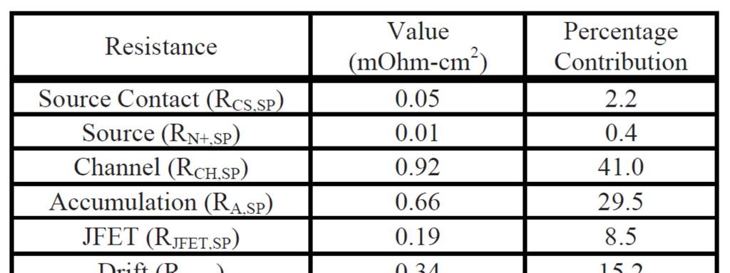
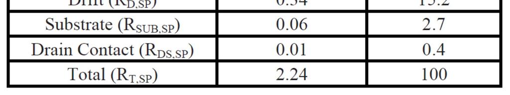
29 D-MOSFET On-Resistance (cont d)

30 U-MOSFET (or trench-gate MOSFET) Structure During the late 1980s, the technology for etching trenches in silicon became available due to its application for making charge storage capacitors within DRAM chips. This process was adapted by the power semiconductor industry to develop the trench-gate or U-MOSFET structure. As shown in figure above, the trench extends from the upper surface of the structure through the N+ source and P-base regions into the N-drift region. The gate electrode is placed within the trench after the formation of the gate oxide by thermal oxidation of the bottom and sidewalls.
31 How a U-MOSFET works? Without the application of a gate bias, a high voltage can be supported in the U-MOSFET structure when a positive bias is applied to the drain. In this case, junction J 1 formed between the P-base region and the N-drift region becomes reverse biased. The voltage is supported mainly within the thick lightly doped N-drift region. Since the gate is at zero potential during the blocking mode of operation, a high electric field is also developed across the gate oxide. To avoid reliability problems arising from the enhanced electric field in the gate oxide at the trench corners, it is customary to round the bottom of the trench. Drain current flow in the U-MOSFET structure is induced by the application of a positive bias to the gate electrode. This produces an inversion layer channel at the surface of the P-base region along the vertical sidewalls of the trench. This inversion layer channel provides a path for transport of electrons from the source to the drain when a positive drain voltage is applied. After transport from the source region through the channel, the electrons enter the N-drift region at the bottom of the trenches. The current then spreads to the entire width of the cell cross section. Consequently, there is no JFET region in the U-MOSFET structure, enabling a significant reduction of the internal resistance when compared with the D-MOSFET structure. The reduced internal resistance for the U-MOSFET structure provided motivation for the development of these devices in the 1990s.

32 U-MOSFET On-Resistance Source Contact Resistance R CS Source Region Resistance R N+ Channel Resistance R CH Accumulation Resistance R A Drift Region Resistance R D Substrate Resistance R SUB Drain Contact Resistance R CD

33 U-MOSFET On-Resistance (cont d)
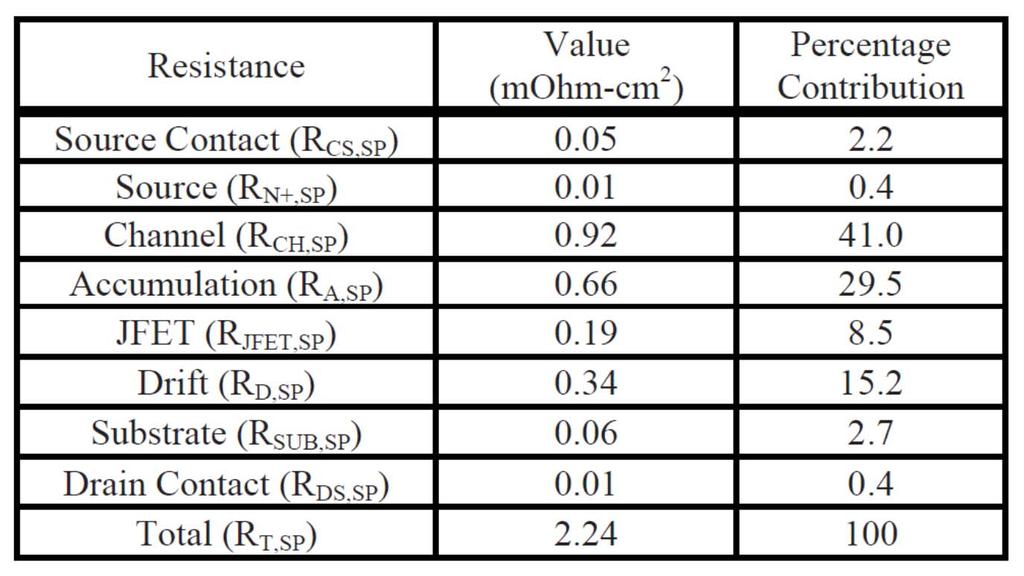
34 On-Resistance: U-MOSFET vs D-MOSFET D-MOSFET U-MOSFET
35 Summary The physics of operation of the power MOSFET structure has been discussed in this chapter. The evolution of the device structural design from the planar-gate D-MOSFET architecture to the trench-gate power U-MOSFET architecture has allowed significant reduction of the specific on-resistance, especially for devices designed to support low blocking voltages. The device structures and working principles of power V-MOSFET, D- MOSFET, and U-MOSFET are discussed. The on-state resistance of D- MOSFET and U-MOSFET are discussed and compared. Sections discussed: 6.1, 6.2, 6.5, 6.8, 6.23 Sections not discussed: 6.3, 6.4, 6.7,
Power Bipolar Junction Transistors (BJTs)
") ECE442 Power Semiconductor Devices and Integrated Circuits Power Bipolar Junction Transistors (BJTs) Zheng Yang (ERF 3017, email: yangzhen@uic.edu) Power Bipolar Junction Transistor (BJT) Background The
ECE442 Power Semiconductor Devices and Integrated Circuits Power Bipolar Junction Transistors (BJTs) Zheng Yang (ERF 3017, email: yangzhen@uic.edu) Power Bipolar Junction Transistor (BJT) Background The
Fundamentals of Power Semiconductor Devices
 В. Jayant Baliga Fundamentals of Power Semiconductor Devices 4y Spri ringer Contents Preface vii Chapter 1 Introduction 1 1.1 Ideal and Typical Power Switching Waveforms 3 1.2 Ideal and Typical Power Device
EE 5611 Introduction to Microelectronic Technologies Fall Thursday, September 04, 2014 Lecture 02
 EE 5611 Introduction to Microelectronic Technologies Fall 2014 Thursday, September 04, 2014 Lecture 02 1 Lecture Outline Review on semiconductor materials Review on microelectronic devices Example of microelectronic
FET(Field Effect Transistor)
") Field Effect Transistor: Construction and Characteristic of JFETs. Transfer Characteristic. CS,CD,CG amplifier and analysis of CS amplifier MOSFET (Depletion and Enhancement) Type, Transfer Characteristic,
Field Effect Transistor: Construction and Characteristic of JFETs. Transfer Characteristic. CS,CD,CG amplifier and analysis of CS amplifier MOSFET (Depletion and Enhancement) Type, Transfer Characteristic,
Three Terminal Devices
 Three Terminal Devices - field effect transistor (FET) - bipolar junction transistor (BJT) - foundation on which modern electronics is built - active devices - devices described completely by considering
UNIT 3: FIELD EFFECT TRANSISTORS
 FIELD EFFECT TRANSISTOR: UNIT 3: FIELD EFFECT TRANSISTORS The field effect transistor is a semiconductor device, which depends for its operation on the control of current by an electric field. There are
Conduction Characteristics of MOS Transistors (for fixed Vds)! Topic 2. Basic MOS theory & SPICE simulation. MOS Transistor
! Topic 2. Basic MOS theory & SPICE simulation. MOS Transistor") Conduction Characteristics of MOS Transistors (for fixed Vds)! Topic 2 Basic MOS theory & SPICE simulation Peter Cheung Department of Electrical & Electronic Engineering Imperial College London (Weste&Harris,
Conduction Characteristics of MOS Transistors (for fixed Vds)! Topic 2 Basic MOS theory & SPICE simulation Peter Cheung Department of Electrical & Electronic Engineering Imperial College London (Weste&Harris,
Topic 2. Basic MOS theory & SPICE simulation
 Topic 2 Basic MOS theory & SPICE simulation Peter Cheung Department of Electrical & Electronic Engineering Imperial College London (Weste&Harris, Ch 2 & 5.1-5.3 Rabaey, Ch 3) URL: www.ee.ic.ac.uk/pcheung/
Conduction Characteristics of MOS Transistors (for fixed Vds) Topic 2. Basic MOS theory & SPICE simulation. MOS Transistor
 Topic 2. Basic MOS theory & SPICE simulation. MOS Transistor") Conduction Characteristics of MOS Transistors (for fixed Vds) Topic 2 Basic MOS theory & SPICE simulation Peter Cheung Department of Electrical & Electronic Engineering Imperial College London (Weste&Harris,
Conduction Characteristics of MOS Transistors (for fixed Vds) Topic 2 Basic MOS theory & SPICE simulation Peter Cheung Department of Electrical & Electronic Engineering Imperial College London (Weste&Harris,
Semiconductor Physics and Devices
 Metal-Semiconductor and Semiconductor Heterojunctions The Metal-Oxide-Semiconductor Field-Effect Transistor (MOSFET) is one of two major types of transistors. The MOSFET is used in digital circuit, because
Integrated diodes. The forward voltage drop only slightly depends on the forward current. ELEKTRONIKOS ĮTAISAI
 1 Integrated diodes pn junctions of transistor structures can be used as integrated diodes. The choice of the junction is limited by the considerations of switching speed and breakdown voltage. The forward
Appendix: Power Loss Calculation
 Appendix: Power Loss Calculation Current flow paths in a synchronous buck converter during on and off phases are illustrated in Fig. 1. It has to be noticed that following parameters are interrelated:
Solid State Devices- Part- II. Module- IV
 Solid State Devices- Part- II Module- IV MOS Capacitor Two terminal MOS device MOS = Metal- Oxide- Semiconductor MOS capacitor - the heart of the MOSFET The MOS capacitor is used to induce charge at the
CONTENTS. 2.2 Schrodinger's Wave Equation 31. PART I Semiconductor Material Properties. 2.3 Applications of Schrodinger's Wave Equation 34
 CONTENTS Preface x Prologue Semiconductors and the Integrated Circuit xvii PART I Semiconductor Material Properties CHAPTER 1 The Crystal Structure of Solids 1 1.0 Preview 1 1.1 Semiconductor Materials
FUNDAMENTALS OF MODERN VLSI DEVICES
 19-13- FUNDAMENTALS OF MODERN VLSI DEVICES YUAN TAUR TAK H. MING CAMBRIDGE UNIVERSITY PRESS Physical Constants and Unit Conversions List of Symbols Preface page xi xiii xxi 1 INTRODUCTION I 1.1 Evolution
PHYSICS OF SEMICONDUCTOR DEVICES
 PHYSICS OF SEMICONDUCTOR DEVICES PHYSICS OF SEMICONDUCTOR DEVICES by J. P. Colinge Department of Electrical and Computer Engineering University of California, Davis C. A. Colinge Department of Electrical
Field-Effect Transistor (FET) is one of the two major transistors; FET derives its name from its working mechanism;
 is one of the two major transistors; FET derives its name from its working mechanism;") Chapter 3 Field-Effect Transistors (FETs) 3.1 Introduction Field-Effect Transistor (FET) is one of the two major transistors; FET derives its name from its working mechanism; The concept has been known
Chapter 3 Field-Effect Transistors (FETs) 3.1 Introduction Field-Effect Transistor (FET) is one of the two major transistors; FET derives its name from its working mechanism; The concept has been known
INTRODUCTION: Basic operating principle of a MOSFET:
 INTRODUCTION: Along with the Junction Field Effect Transistor (JFET), there is another type of Field Effect Transistor available whose Gate input is electrically insulated from the main current carrying
NAME: Last First Signature
 UNIVERSITY OF CALIFORNIA, BERKELEY College of Engineering Department of Electrical Engineering and Computer Sciences EE 130: IC Devices Spring 2003 FINAL EXAMINATION NAME: Last First Signature STUDENT
Digital Electronics. By: FARHAD FARADJI, Ph.D. Assistant Professor, Electrical and Computer Engineering, K. N. Toosi University of Technology
 K. N. Toosi University of Technology Chapter 7. Field-Effect Transistors By: FARHAD FARADJI, Ph.D. Assistant Professor, Electrical and Computer Engineering, K. N. Toosi University of Technology http://wp.kntu.ac.ir/faradji/digitalelectronics.htm
Advanced Power MOSFET Concepts
 В. Jayant Baliga Advanced Power MOSFET Concepts Springer Contents 1 Introduction 1 1.1 Ideal Power Switching Waveforms 2 1.2 Ideal and Typical Power MOSFET Characteristics 3 1.3 Typical Power MOSFET Structures
I E I C since I B is very small
 Figure 2: Symbols and nomenclature of a (a) npn and (b) pnp transistor. The BJT consists of three regions, emitter, base, and collector. The emitter and collector are usually of one type of doping, while
4H-SiC V-Groove Trench MOSFETs with the Buried p + Regions
 ELECTRONICS 4H-SiC V-Groove Trench MOSFETs with the Buried p + Regions Yu SAITOH*, Toru HIYOSHI, Keiji WADA, Takeyoshi MASUDA, Takashi TSUNO and Yasuki MIKAMURA ----------------------------------------------------------------------------------------------------------------------------------------------------------------------------------------------------------------------------------------------------------
Students: Yifan Jiang (Research Assistant) Siyang Liu (Visiting Scholar)
 Siyang Liu (Visiting Scholar)") Y9.FS1.1: SiC Power Devices for SST Applications Project Leader: Faculty: Dr. Jayant Baliga Dr. Alex Huang Students: Yifan Jiang (Research Assistant) Siyang Liu (Visiting Scholar) 1. Project Goals (a)
Y9.FS1.1: SiC Power Devices for SST Applications Project Leader: Faculty: Dr. Jayant Baliga Dr. Alex Huang Students: Yifan Jiang (Research Assistant) Siyang Liu (Visiting Scholar) 1. Project Goals (a)
Mechanis m Faliures. Group Leader Jepsy 1)Substrate Biasing 2) Minority Injection. Bob 1)Minority-Carrier Guard Rings
Substrate Biasing 2) Minority Injection. Bob 1)Minority-Carrier Guard Rings") Mechanis m Faliures Group Leader Jepsy 1)Substrate Biasing 2) Minority Injection As im 1)Types Of Guard Rings Sandra 1)Parasitics 2)Field Plating Bob 1)Minority-Carrier Guard Rings Shawn 1)Parasitic Channel
Mechanis m Faliures Group Leader Jepsy 1)Substrate Biasing 2) Minority Injection As im 1)Types Of Guard Rings Sandra 1)Parasitics 2)Field Plating Bob 1)Minority-Carrier Guard Rings Shawn 1)Parasitic Channel
MOSFET short channel effects
 MOSFET short channel effects overview Five different short channel effects can be distinguished: velocity saturation drain induced barrier lowering (DIBL) impact ionization surface scattering hot electrons
Key Questions. ECE 340 Lecture 39 : Introduction to the BJT-II 4/28/14. Class Outline: Fabrication of BJTs BJT Operation
 Things you should know when you leave ECE 340 Lecture 39 : Introduction to the BJT-II Fabrication of BJTs Class Outline: Key Questions What elements make up the base current? What do the carrier distributions
UNIT-VI FIELD EFFECT TRANSISTOR. 1. Explain about the Field Effect Transistor and also mention types of FET s.
 UNIT-I FIELD EFFECT TRANSISTOR 1. Explain about the Field Effect Transistor and also mention types of FET s. The Field Effect Transistor, or simply FET however, uses the voltage that is applied to their
value of W max for the device. The at band voltage is -0.9 V. Problem 5: An Al-gate n-channel MOS capacitor has a doping of N a = cm ;3. The oxi
 Prof. Jasprit Singh Fall 2001 EECS 320 Homework 10 This homework is due on December 6 Problem 1: An n-type In 0:53 Ga 0:47 As epitaxial layer doped at 10 16 cm ;3 is to be used as a channel in a FET. A
ECE 340 Lecture 37 : Metal- Insulator-Semiconductor FET Class Outline:
 ECE 340 Lecture 37 : Metal- Insulator-Semiconductor FET Class Outline: Metal-Semiconductor Junctions MOSFET Basic Operation MOS Capacitor Things you should know when you leave Key Questions What is the
Semiconductor Devices
 Semiconductor Devices Modelling and Technology Source Electrons Gate Holes Drain Insulator Nandita DasGupta Amitava DasGupta SEMICONDUCTOR DEVICES Modelling and Technology NANDITA DASGUPTA Professor Department
Sub-Threshold Region Behavior of Long Channel MOSFET
 Sub-threshold Region - So far, we have discussed the MOSFET behavior in linear region and saturation region - Sub-threshold region is refer to region where Vt is less than Vt - Sub-threshold region reflects
AE53/AC53/AT53/AE103 ELECT. DEVICES & CIRCUITS DEC 2015
 Q.2 a. By using Norton s theorem, find the current in the load resistor R L for the circuit shown in Fig.1. (8) Fig.1 IETE 1 b. Explain Z parameters and also draw an equivalent circuit of the Z parameter
ITT Technical Institute. ET215 Devices 1. Unit 8 Chapter 4, Sections
 ITT Technical Institute ET215 Devices 1 Unit 8 Chapter 4, Sections 4.4 4.5 Chapter 4 Section 4.4 MOSFET Characteristics A Metal-Oxide semiconductor field-effect transistor is the other major category of
The Art of ANALOG LAYOUT Second Edition
 The Art of ANALOG LAYOUT Second Edition Alan Hastings 3 EARSON Pearson Education International Contents Preface to the Second Edition xvii Preface to the First Edition xix Acknowledgments xxi 1 Device
CHAPTER I INTRODUCTION
 CHAPTER I INTRODUCTION High performance semiconductor devices with better voltage and current handling capability are required in different fields like power electronics, computer and automation. Since
Chapter 8. Field Effect Transistor
 Chapter 8. Field Effect Transistor Field Effect Transistor: The field effect transistor is a semiconductor device, which depends for its operation on the control of current by an electric field. There
Power Semiconductor Devices
 TRADEMARK OF INNOVATION Power Semiconductor Devices Introduction This technical article is dedicated to the review of the following power electronics devices which act as solid-state switches in the circuits.
ECE520 VLSI Design. Lecture 2: Basic MOS Physics. Payman Zarkesh-Ha
 ECE520 VLSI Design Lecture 2: Basic MOS Physics Payman Zarkesh-Ha Office: ECE Bldg. 230B Office hours: Wednesday 2:00-3:00PM or by appointment E-mail: pzarkesh@unm.edu Slide: 1 Review of Last Lecture Semiconductor
ELECTRONIC DEVICES AND CIRCUITS
 ELECTRONIC DEVICES AND CIRCUITS 1. At room temperature the current in an intrinsic semiconductor is due to A. holes B. electrons C. ions D. holes and electrons 2. Work function is the maximum energy required
Progress Energy Distinguished University Professor Jay Baliga. April 11, Acknowledgements
 Progress Energy Distinguished University Professor Jay Baliga April 11, 2019 Acknowledgements 1 Outline SiC Power MOSFET Breakthroughs achieved at NCSU PRESiCE: SiC Power Device Manufacturing Technology
EE301 Electronics I , Fall
 EE301 Electronics I 2018-2019, Fall 1. Introduction to Microelectronics (1 Week/3 Hrs.) Introduction, Historical Background, Basic Consepts 2. Rewiev of Semiconductors (1 Week/3 Hrs.) Semiconductor materials
Impact of Basal Plane Dislocations and Ruggedness of 10 kv 4H-SiC Transistors
 11th International MOS-AK Workshop (co-located with the IEDM and CMC Meetings) Silicon Valley, December 5, 2018 Impact of Basal Plane Dislocations and Ruggedness of 10 kv 4H-SiC Transistors *, A. Kumar,
Solid State Device Fundamentals
 Solid State Device Fundamentals 4.4. Field Effect Transistor (MOSFET) ENS 463 Lecture Course by Alexander M. Zaitsev alexander.zaitsev@csi.cuny.edu Tel: 718 982 2812 4N101b 1 Field-effect transistor (FET)
Wide Band-Gap Power Device
 Wide Band-Gap Power Device 1 Contents Revisit silicon power MOSFETs Silicon limitation Silicon solution Wide Band-Gap material Characteristic of SiC Power Device Characteristic of GaN Power Device 2 1
USING F-SERIES IGBT MODULES
 .0 Introduction Mitsubishi s new F-series IGBTs represent a significant advance over previous IGBT generations in terms of total power losses. The device remains fundamentally the same as a conventional
ADVANCED POWER RECTIFIER CONCEPTS
 ADVANCED POWER RECTIFIER CONCEPTS B. Jayant Baliga ADVANCED POWER RECTIFIER CONCEPTS B. Jayant Baliga Power Semiconductor Research Center North Carolina State University Raleigh, NC 27695-7924, USA bjbaliga@unity.ncsu.edu
INTRODUCTION TO MOS TECHNOLOGY
 INTRODUCTION TO MOS TECHNOLOGY 1. The MOS transistor The most basic element in the design of a large scale integrated circuit is the transistor. For the processes we will discuss, the type of transistor
VLSI Technology Dr. Nandita Dasgupta Department of Electrical Engineering Indian Institute of Technology, Madras
 VLSI Technology Dr. Nandita Dasgupta Department of Electrical Engineering Indian Institute of Technology, Madras Lecture - 40 BICMOS technology So, today we are going to have the last class on this VLSI
Lecture - 18 Transistors
 Electronic Materials, Devices and Fabrication Dr. S. Prarasuraman Department of Metallurgical and Materials Engineering Indian Institute of Technology, Madras Lecture - 18 Transistors Last couple of classes
Transistor was first invented by William.B.Shockley, Walter Brattain and John Bardeen of Bell Labratories. In 1961, first IC was introduced.
 Unit 1 Basic MOS Technology Transistor was first invented by William.B.Shockley, Walter Brattain and John Bardeen of Bell Labratories. In 1961, first IC was introduced. Levels of Integration:- i) SSI:-
In this lecture we will begin a new topic namely the Metal-Oxide-Semiconductor Field Effect Transistor.
 Solid State Devices Dr. S. Karmalkar Department of Electronics and Communication Engineering Indian Institute of Technology, Madras Lecture - 38 MOS Field Effect Transistor In this lecture we will begin
Open Access. C.H. Ho 1, F.T. Chien 2, C.N. Liao 1 and Y.T. Tsai*,1
 56 The Open Electrical and Electronic Engineering Journal, 2008, 2, 56-61 Open Access Optimum Design for Eliminating Back Gate Bias Effect of Silicon-oninsulator Lateral Double Diffused Metal-oxide-semiconductor
Laboratory #5 BJT Basics and MOSFET Basics
 Laboratory #5 BJT Basics and MOSFET Basics I. Objectives 1. Understand the physical structure of BJTs and MOSFETs. 2. Learn to measure I-V characteristics of BJTs and MOSFETs. II. Components and Instruments
Semiconductor Memory: DRAM and SRAM. Department of Electrical and Computer Engineering, National University of Singapore
 Semiconductor Memory: DRAM and SRAM Outline Introduction Random Access Memory (RAM) DRAM SRAM Non-volatile memory UV EPROM EEPROM Flash memory SONOS memory QD memory Introduction Slow memories Magnetic
KOREA UNIVERSITY. Photonics Laboratory. Ch 15. Field effect Introduction-The J-FET and MESFET
 Ch 15. Field effect Introduction-The J-FET and MESFET : (a) The device worked on the principle that a voltage applied to the metallic plate modulated the conductance of the underlying semiconductor, which
Some Key Researches on SiC Device Technologies and their Predicted Advantages
 18 POWER SEMICONDUCTORS www.mitsubishichips.com Some Key Researches on SiC Device Technologies and their Predicted Advantages SiC has proven to be a good candidate as a material for next generation power
Unit III FET and its Applications. 2 Marks Questions and Answers
 Unit III FET and its Applications 2 Marks Questions and Answers 1. Why do you call FET as field effect transistor? The name field effect is derived from the fact that the current is controlled by an electric
Lecture 19 Real Semiconductor Switches and the Evolution of Power MOSFETS A.. Real Switches: I(D) through the switch and V(D) across the switch
 through the switch and V(D) across the switch") Lecture 19 Real Semiconductor Switches and the Evolution of Power MOSFETS 1 A.. Real Switches: I(D) through the switch and V(D) across the switch 1. Two quadrant switch implementation and device choice
Lecture 19 Real Semiconductor Switches and the Evolution of Power MOSFETS 1 A.. Real Switches: I(D) through the switch and V(D) across the switch 1. Two quadrant switch implementation and device choice
Chapter 9 SiC Planar MOSFET Structures
 Chapter 9 SiC Planar MOSFET Structures In Chap. 1, it was demonstrated that the specific on-resistance of power MOSFET devices can be greatly reduced by replacing silicon with wide band gap semiconductors.
Field Effect Transistors (npn)
") Field Effect Transistors (npn) gate drain source FET 3 terminal device channel e - current from source to drain controlled by the electric field generated by the gate base collector emitter BJT 3 terminal
Field Effect Transistors (npn) gate drain source FET 3 terminal device channel e - current from source to drain controlled by the electric field generated by the gate base collector emitter BJT 3 terminal
L MOSFETS, IDENTIFICATION, CURVES. PAGE 1. I. Review of JFET (DRAW symbol for n-channel type, with grounded source)
") L.107.4 MOSFETS, IDENTIFICATION, CURVES. PAGE 1 I. Review of JFET (DRAW symbol for n-channel type, with grounded source) 1. "normally on" device A. current from source to drain when V G = 0 no need to
L.107.4 MOSFETS, IDENTIFICATION, CURVES. PAGE 1 I. Review of JFET (DRAW symbol for n-channel type, with grounded source) 1. "normally on" device A. current from source to drain when V G = 0 no need to
Power MOSFET Basics. Table of Contents. 2. Breakdown Voltage. 1. Basic Device Structure. 3. On-State Characteristics
 Power MOSFET Basics Table of Contents P-body N + Source Gate N - Epi 1. Basic Device Structure 2. Breakdown Voltage 3. On-State Characteristics 4. Capacitance 5. Gate Charge 6. Gate Resistance 7. Turn-on
Lecture 3: Transistors
 Lecture 3: Transistors Now that we know about diodes, let s put two of them together, as follows: collector base emitter n p n moderately doped lightly doped, and very thin heavily doped At first glance,
Lecture 020 ECE4430 Review II (1/5/04) Page 020-1
 Page 020-1") Lecture 020 ECE4430 Review II (1/5/04) Page 020-1 LECTURE 020 ECE 4430 REVIEW II (READING: GHLM - Chap. 2) Objective The objective of this presentation is: 1.) Identify the prerequisite material as taught
Lecture 020 ECE4430 Review II (1/5/04) Page 020-1 LECTURE 020 ECE 4430 REVIEW II (READING: GHLM - Chap. 2) Objective The objective of this presentation is: 1.) Identify the prerequisite material as taught
UNIT 3 Transistors JFET
 UNIT 3 Transistors JFET Mosfet Definition of BJT A bipolar junction transistor is a three terminal semiconductor device consisting of two p-n junctions which is able to amplify or magnify a signal. It
Lecture 020 ECE4430 Review II (1/5/04) Page 020-1
 Page 020-1") Lecture 020 ECE4430 Review II (1/5/04) Page 020-1 LECTURE 020 ECE 4430 REVIEW II (READING: GHLM - Chap. 2) Objective The objective of this presentation is: 1.) Identify the prerequisite material as taught
Lecture 020 ECE4430 Review II (1/5/04) Page 020-1 LECTURE 020 ECE 4430 REVIEW II (READING: GHLM - Chap. 2) Objective The objective of this presentation is: 1.) Identify the prerequisite material as taught
Substrate Bias Effects on Drain Induced Barrier Lowering (DIBL) in Short Channel NMOS FETs
 in Short Channel NMOS FETs") Australian Journal of Basic and Applied Sciences, 3(3): 1640-1644, 2009 ISSN 1991-8178 Substrate Bias Effects on Drain Induced Barrier Lowering (DIBL) in Short Channel NMOS FETs 1 1 1 1 2 A. Ruangphanit,
Australian Journal of Basic and Applied Sciences, 3(3): 1640-1644, 2009 ISSN 1991-8178 Substrate Bias Effects on Drain Induced Barrier Lowering (DIBL) in Short Channel NMOS FETs 1 1 1 1 2 A. Ruangphanit,
Session 3: Solid State Devices. Silicon on Insulator
 Session 3: Solid State Devices Silicon on Insulator 1 Outline A B C D E F G H I J 2 Outline Ref: Taurand Ning 3 SOI Technology SOl materials: SIMOX, BESOl, and Smart Cut SIMOX : Synthesis by IMplanted
Notes. (Subject Code: 7EC5)
") COMPUCOM INSTITUTE OF TECHNOLOGY & MANAGEMENT, JAIPUR (DEPARTMENT OF ELECTRONICS & COMMUNICATION) Notes VLSI DESIGN NOTES (Subject Code: 7EC5) Prepared By: MANVENDRA SINGH Class: B. Tech. IV Year, VII
COMPUCOM INSTITUTE OF TECHNOLOGY & MANAGEMENT, JAIPUR (DEPARTMENT OF ELECTRONICS & COMMUNICATION) Notes VLSI DESIGN NOTES (Subject Code: 7EC5) Prepared By: MANVENDRA SINGH Class: B. Tech. IV Year, VII
MSE 410/ECE 340: Electrical Properties of Materials Fall 2016 Micron School of Materials Science and Engineering Boise State University
 MSE 410/ECE 340: Electrical Properties of Materials Fall 2016 Micron School of Materials Science and Engineering Boise State University Practice Final Exam 1 Read the questions carefully Label all figures
The Common Source JFET Amplifier
 The Common Source JFET Amplifier Small signal amplifiers can also be made using Field Effect Transistors or FET's for short. These devices have the advantage over bipolar transistors of having an extremely
Review Energy Bands Carrier Density & Mobility Carrier Transport Generation and Recombination
 Review Energy Bands Carrier Density & Mobility Carrier Transport Generation and Recombination Current Transport: Diffusion, Thermionic Emission & Tunneling For Diffusion current, the depletion layer is
Analog and Telecommunication Electronics
 Politecnico di Torino - ICT School Analog and Telecommunication Electronics F2 Active power devices»mos»bjt» IGBT, TRIAC» Safe Operating Area» Thermal analysis 30/05/2012-1 ATLCE - F2-2011 DDC Lesson F2:
FIELD EFFECT TRANSISTOR (FET) 1. JUNCTION FIELD EFFECT TRANSISTOR (JFET)
 1. JUNCTION FIELD EFFECT TRANSISTOR (JFET)") FIELD EFFECT TRANSISTOR (FET) The field-effect transistor (FET) is a three-terminal device used for a variety of applications that match, to a large extent, those of the BJT transistor. Although there
FIELD EFFECT TRANSISTOR (FET) The field-effect transistor (FET) is a three-terminal device used for a variety of applications that match, to a large extent, those of the BJT transistor. Although there
Lecture 15. Field Effect Transistor (FET) Wednesday 29/11/2017 MOSFET 1-1
 Wednesday 29/11/2017 MOSFET 1-1") Lecture 15 Field Effect Transistor (FET) Wednesday 29/11/2017 MOSFET 1-1 Outline MOSFET transistors Introduction to MOSFET MOSFET Types epletion-type MOSFET Characteristics Comparison between JFET and
Lecture 15 Field Effect Transistor (FET) Wednesday 29/11/2017 MOSFET 1-1 Outline MOSFET transistors Introduction to MOSFET MOSFET Types epletion-type MOSFET Characteristics Comparison between JFET and
Exam Below are two schematics of current sources implemented with MOSFETs. Which current source has the best compliance voltage?
 Exam 2 Name: Score /90 Question 1 Short Takes 1 point each unless noted otherwise. 1. Below are two schematics of current sources implemented with MOSFETs. Which current source has the best compliance
Semiconductor Devices
 Semiconductor Devices - 2014 Lecture Course Part of SS Module PY4P03 Dr. P. Stamenov School of Physics and CRANN, Trinity College, Dublin 2, Ireland Hilary Term, TCD 3 th of Feb 14 MOSFET Unmodified Channel
Chapter 2 : Semiconductor Materials & Devices (II) Feb
 Feb") Chapter 2 : Semiconductor Materials & Devices (II) 1 Reference 1. SemiconductorManufacturing Technology: Michael Quirk and Julian Serda (2001) 3. Microelectronic Circuits (5/e): Sedra & Smith (2004) 4.
Chapter 2 : Semiconductor Materials & Devices (II) 1 Reference 1. SemiconductorManufacturing Technology: Michael Quirk and Julian Serda (2001) 3. Microelectronic Circuits (5/e): Sedra & Smith (2004) 4.
Depletion-mode operation ( 공핍형 ): Using an input gate voltage to effectively decrease the channel size of an FET
: Using an input gate voltage to effectively decrease the channel size of an FET") Ch. 13 MOSFET Metal-Oxide-Semiconductor Field-Effect Transistor : I D D-mode E-mode V g The gate oxide is made of dielectric SiO 2 with e = 3.9 Depletion-mode operation ( 공핍형 ): Using an input gate voltage
Ch. 13 MOSFET Metal-Oxide-Semiconductor Field-Effect Transistor : I D D-mode E-mode V g The gate oxide is made of dielectric SiO 2 with e = 3.9 Depletion-mode operation ( 공핍형 ): Using an input gate voltage
PHYS 3050 Electronics I
 PHYS 3050 Electronics I Chapter 4. Semiconductor Diodes and Transistors Earth, Moon, Mars, and Beyond Dr. Jinjun Shan, Associate Professor of Space Engineering Department of Earth and Space Science and
VIRTUAL FABRICATION PROCESS OF PLANAR POWER MOSFET USING SILVACO TCAD TOOLS NORZAKIAH BINTI ZAHARI
 VIRTUAL FABRICATION PROCESS OF PLANAR POWER MOSFET USING SILVACO TCAD TOOLS NORZAKIAH BINTI ZAHARI This Report Is Submitted In Partial Fulfilment of Requirements For The Bachelor Degree of Electronic Engineering
EFM Ec. a) Sketch the electrostatic potential inside the semiconductor as a function of position.
 Sketch the electrostatic potential inside the semiconductor as a function of position.") 1.The energy band diagram for an ideal x o =.2um MOS-C operated at T=300K is shown below. Note that the applied gate voltage causes band bending in the semiconductor such that E F =E i at the Si-SiO2 interface.
1.The energy band diagram for an ideal x o =.2um MOS-C operated at T=300K is shown below. Note that the applied gate voltage causes band bending in the semiconductor such that E F =E i at the Si-SiO2 interface.
Power Devices and ICs Chapter 15
 Power Devices and ICs Chapter 15 Syed Asad Alam DA, ISY 4/28/2015 1 Overview 4/28/2015 2 Overview Types of Power Devices PNPN Thyristor TRIAC (Triode Alternating Current) GTO (Gate Turn-Off Thyristor)
Lecture 4 -- Tuesday, Sept. 19: Non-uniform injection and/or doping. Diffusion. Continuity/conservation. The five basic equations.
 6.012 ELECTRONIC DEVICES AND CIRCUITS Schedule -- Fall 1995 (8/31/95 version) Recitation 1 -- Wednesday, Sept. 6: Review of 6.002 models for BJT. Discussion of models and modeling; motivate need to go
Quantum Condensed Matter Physics Lecture 16
 Quantum Condensed Matter Physics Lecture 16 David Ritchie QCMP Lent/Easter 2018 http://www.sp.phy.cam.ac.uk/drp2/home 16.1 Quantum Condensed Matter Physics 1. Classical and Semi-classical models for electrons
EE70 - Intro. Electronics
 EE70 - Intro. Electronics Course website: ~/classes/ee70/fall05 Today s class agenda (November 28, 2005) review Serial/parallel resonant circuits Diode Field Effect Transistor (FET) f 0 = Qs = Qs = 1 2π
AE103 ELECTRONIC DEVICES & CIRCUITS DEC 2014
 Q.2 a. State and explain the Reciprocity Theorem and Thevenins Theorem. a. Reciprocity Theorem: If we consider two loops A and B of network N and if an ideal voltage source E in loop A produces current
Lecture 13. Metal Oxide Semiconductor Field Effect Transistor (MOSFET) MOSFET 1-1
 MOSFET 1-1") Lecture 13 Metal Oxide Semiconductor Field Effect Transistor (MOSFET) MOSFET 1-1 Outline Continue MOSFET Qualitative Operation epletion-type MOSFET Characteristics Biasing Circuits and Examples Enhancement-type
Lecture 13 Metal Oxide Semiconductor Field Effect Transistor (MOSFET) MOSFET 1-1 Outline Continue MOSFET Qualitative Operation epletion-type MOSFET Characteristics Biasing Circuits and Examples Enhancement-type
IGBT Module Chip Improvements for Industrial Motor Drives
 IGBT Module Chip Improvements for Industrial Motor Drives John F. Donlon Powerex, Inc. 173 Pavilion Lane Youngwood, PA USA Katsumi Satoh Mitsubishi Electric Corporation Power Semiconductor Device Works
ELEC-E8421 Components of Power Electronics
 ELEC-E8421 Components of Power Electronics MOSFET 2015-10-04 Metal-Oxide-Semiconductor Field-Effect-Transistor (MOSFET) Vertical structure makes paralleling of many small MOSFETs on the chip easy. Very
Study on Fabrication and Fast Switching of High Voltage SiC JFET
 Advanced Materials Research Online: 2013-10-31 ISSN: 1662-8985, Vol. 827, pp 282-286 doi:10.4028/www.scientific.net/amr.827.282 2014 Trans Tech Publications, Switzerland Study on Fabrication and Fast Switching
MOSFET & IC Basics - GATE Problems (Part - I)
") MOSFET & IC Basics - GATE Problems (Part - I) 1. Channel current is reduced on application of a more positive voltage to the GATE of the depletion mode n channel MOSFET. (True/False) [GATE 1994: 1 Mark]
MOSFET & IC Basics - GATE Problems (Part - I) 1. Channel current is reduced on application of a more positive voltage to the GATE of the depletion mode n channel MOSFET. (True/False) [GATE 1994: 1 Mark]
Modeling And Optimization Of Body Diode Reverse Recovery Characteristics Of Ldmos Transistors
 University of Central Florida Electronic Theses and Dissertations Masters Thesis (Open Access) Modeling And Optimization Of Body Diode Reverse Recovery Characteristics Of Ldmos Transistors 2006 Wesley
Design cycle for MEMS
 Design cycle for MEMS Design cycle for ICs IC Process Selection nmos CMOS BiCMOS ECL for logic for I/O and driver circuit for critical high speed parts of the system The Real Estate of a Wafer MOS Transistor
FET. Field Effect Transistors ELEKTRONIKA KONTROL. Eka Maulana, ST, MT, M.Eng. Universitas Brawijaya. p + S n n-channel. Gate. Basic structure.
 FET Field Effect Transistors ELEKTRONIKA KONTROL Basic structure Gate G Source S n n-channel Cross section p + p + p + G Depletion region Drain D Eka Maulana, ST, MT, M.Eng. Universitas Brawijaya S Channel
Semiconductor TCAD Tools
 Device Design Consideration for Nanoscale MOSFET Using Semiconductor TCAD Tools Teoh Chin Hong and Razali Ismail Department of Microelectronics and Computer Engineering, Universiti Teknologi Malaysia,
SRM INSTITUTE OF SCIENCE AND TECHNOLOGY (DEEMED UNIVERSITY)
") SRM INSTITUTE OF SCIENCE AND TECHNOLOGY (DEEMED UNIVERSITY) QUESTION BANK I YEAR B.Tech (II Semester) ELECTRONIC DEVICES (COMMON FOR EC102, EE104, IC108, BM106) UNIT-I PART-A 1. What are intrinsic and
SRM INSTITUTE OF SCIENCE AND TECHNOLOGY (DEEMED UNIVERSITY) QUESTION BANK I YEAR B.Tech (II Semester) ELECTRONIC DEVICES (COMMON FOR EC102, EE104, IC108, BM106) UNIT-I PART-A 1. What are intrinsic and
Department of Electrical Engineering IIT Madras
 Department of Electrical Engineering IIT Madras Sample Questions on Semiconductor Devices EE3 applicants who are interested to pursue their research in microelectronics devices area (fabrication and/or
Integrated Circuits: FABRICATION & CHARACTERISTICS - 4. Riju C Issac
 Integrated Circuits: FABRICATION & CHARACTERISTICS - 4 Riju C Issac INTEGRATED RESISTORS Resistor in a monolithic IC is very often obtained by the bulk resistivity of one of the diffused areas. P-type