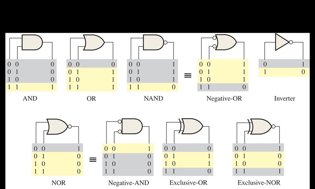
Digital Fundamentals
|
|
|
- Linda Bradley
- 5 years ago
- Views:
Transcription
1 07/ago/2017 Digital Fundamentals ELEVENTH EDITION CHPTER 1 Introductory Concepts
. bit can have the value of either a 0 or a 1, depending on if the voltage is HIGH or LOW.")
2 Digital electronics uses circuits that have two states, which are represented by two different voltage levels called HIGH and LOW. The voltages represent numbers in the binary system. In binary, a single number is called a bit (for binary digit). bit can have the value of either a 0 or a 1, depending on if the voltage is HIGH or LOW. FIGURE 1-6 Logic level ranges of voltage for a digital circuit.
3 Digital waveforms change between the LOW and HIGH levels. positive going pulse is one that goes from a normally LOW logic level to a HIGH level and then back again. Digital waveforms are made up of a series of pulses. FIGURE 1-7 Ideal pulses.
4 ctual pulses are not ideal but are described by the rise time, fall time, amplitude, and other characteristics. FIGURE 1-8 Nonideal pulse characteristics.
5 FIGURE 1-9 Examples of digital waveforms. In addition to frequency and period, repetitive pulse waveforms are described by the amplitude (), pulse width (t W ) and duty cycle. Duty cycle is the ratio of t W to T. Volts mplitude () Pulse width (t W ) Period, T Time
6 Periodic pulse waveforms are composed of pulses that repeats in a fixed interval called the period. The frequency is the rate it repeats and is measured in hertz. f = 1 T T = 1 f The clock is a basic timing signal that is an example of a periodic wave. What is the period of a repetitive wave if f = 3.2 GHz? T = 1 f = GHz = 313 ns
7 Digital Fundamentals ELEVENTH EDITION CHPTER 3 Logic Gates
8 The Inverter FIGURE 3-1 Standard logic symbols for the inverter (NSI/IEEE Std /Std. 91a-1991).
9 The Inverter The inverter performs the oolean NOT operation. When the input is LOW, the output is HIGH; when the input is HIGH, the output is LOW. Input Output LOW (0) HIGH (1) HIGH (1) LOW(0) The NOT operation (complement) is shown with an overbar. Thus, the oolean expression for an inverter is =.
10 The Inverter Example waveforms: group of inverters can be used to form the 1 s complement of a binary number: inary number s complement
11 The ND gate FIGURE 3-8 Standard logic symbols for the ND gate showing two inputs (NSI/IEEE Std /Std. 91a- 1991).
12 The ND gate The ND gate produces a HIGH output when all inputs are HIGH; otherwise, the output is LOW. For a 2-input gate, the truth table is Inputs Output The ND operation is usually shown with a dot between the variables but it may be implied (no dot). Thus, the ND operation is written as =. or =
13 The ND gate FIGURE 3-10 Example of ND gate operation with a timing diagram showing input and output relationships.
14 The ND gate Example waveforms: The ND operation is used in computer programming as a selective mask. If you want to retain certain bits of a binary number but reset the other bits to 0, you could set a mask with 1 s in the position of the retained bits. If the binary number is NDed with the mask , what is the result?
15 The ND gate Waveform for? FIGURE 3-13
16 The ND gate FIGURE 3-15 oolean expressions for ND gates with two, three, and four inputs.
17 The OR gate 1 The OR gate produces a HIGH output if any input is HIGH; if all inputs are LOW, the output is LOW. For a 2-input gate, the truth table is Inputs Output The OR operation is shown with a plus sign (+) between the variables. Thus, the OR operation is written as = +.
18 The OR gate Example waveforms: The OR operation can be used in computer programming to set certain bits of a binary number to 1. SCII letters have a 1 in the bit 5 position for lower case letters and a 0 in this position for capitals. (it positions are numbered from right to left starting with 0.) What will be the result if you OR an SCII letter with the 8-bit mask ? The resulting letter will be lower case.
19 The OR gate FIGURE 3-23
20 The OR gate FIGURE 3-24 oolean expressions for OR gates with two, three, and four inputs.
21 The NND gate & The NND gate produces a LOW output when all inputs are HIGH; otherwise, the output is HIGH. For a 2-input gate, the truth table is Inputs Output The NND operation is shown with a dot between the variables and an overbar covering them. Thus, the NND operation is written as =. (alternatively, = )
22 The NND gate Example waveforms: The NND gate is particularly useful because it is a universal gate all other basic gates can be constructed from NND gates. 2-input NND gate with both inputs connected together is equivalent to which gate?
23 The NND gate The output waveform is LOW only when all three input waveforms are HIGH as shown in the timing diagram. FIGURE 3-29
24 The NOR gate 1 The NOR gate produces a LOW output if any input is HIGH; if all inputs are HIGH, the output is LOW. For a 2-input gate, the truth table is Inputs Output The NOR operation is shown with a plus sign (+) between the variables and an overbar covering them. Thus, the NOR operation is written as = +.
25 The NOR gate Example waveforms: The NOR operation will produce a LOW if any input is HIGH. When is the LED is ON for the circuit shown? +5.0 V 330 W The LED will be on when any of the four inputs are HIGH. C D
26 The NOR gate FIGURE 3-37
27 The OR gate = 1 The OR gate produces a HIGH output only when both inputs are at opposite logic levels. The truth table is Inputs Output The OR operation is written as = +. lternatively, it can be written with a circled plus sign between the variables as = +.
28 The OR gate Example waveforms: Notice that the OR gate will produce a HIGH only when exactly one input is HIGH. If the and waveforms are both inverted for the above waveforms, how is the output affected? There is no change in the output.
29 The OR gate a b c d OR or de n entradas: - 1 quando número de bits é impar - Corresponde à soma dos bits
30 The NOR Gate = 1 The NOR gate produces a HIGH output only when both inputs are at the same logic level. The truth table is Inputs Output The NOR operation shown as = +. lternatively, the NOR operation can be shown with a circled dot between the variables. Thus, it can be shown as =
31 FIGURE 3-48
32 TLE 3 13 n OR gate used to add two bits.


33 Resumão das Portas
34 Transformações entre Representações Lógicas

35 Transformações entre Representações Lógicas

36 [John_R._Gregg]_Ones_and_Zeros_Understanding_ool(ookZZ.org)
37 [John_R._Gregg]_Ones_and_Zeros_Understanding_ool(ookZZ.org)
38 Examine the conditions indicated in Figure 3 92, and identify the faulty gates.
39 Simplificação Lógica Lógica simplificada == hardware mais eficiente Menor área de hardware Menor o atraso da lógica Próximo conteúdo: simplificação lógica.
Digital Fundamentals 8/29/2016. Summary. Summary. Floyd. Chapter 3 A X. The Inverter
 Digital Fundamentals Tenth Edition Floyd Chapter 3 The Inverter The inverter performs the oolean NOT operation. When the input is LOW, the output is HIGH; when the input is HIGH, the output is LOW. Input
Digital Fundamentals 9/4/2017. Summary. Summary. Floyd. Chapter 3. The Inverter
 Digital Fundamentals Tenth Edition Floyd Chapter 3 29 Pearson Education, Upper 28 Pearson Saddle River, Education NJ 7458. ll Rights Reserved The Inverter The inverter performs the oolean NOT operation.
Digital Fundamentals
 Digital Fundamentals Tenth Edition Floyd Chapter 3 28 Pearson Education 29 Pearson Education, Upper Saddle River, NJ 7458. ll Rights Reserved The Inverter The inverter performs the oolean NOT operation.
2 Logic Gates THE INVERTER. A logic gate is an electronic circuit which makes logic decisions. It has one output and one or more inputs.
 2 Logic Gates A logic gate is an electronic circuit which makes logic decisions. It has one output and one or more inputs. THE INVERTER The inverter (NOT circuit) performs the operation called inversion
This Figure here illustrates the operation for a 2-input OR gate for all four possible input combinations.
 Course: B.Sc. Applied Physical Science (Computer Science) Year & Sem.: IInd Year, Sem - IIIrd Subject: Computer Science Paper No.: IX Paper Title: Computer System Architecture Lecture No.: 5 Lecture Title:
Digital Fundamentals
 Digital Fundamentals Tenth Edition Floyd hapter 5 Floyd, Digital Fundamentals, th ed 28 Pearson Education 29 Pearson Education, Upper Saddle River, NJ 7458. ll Rights Reserved ombinational Logic ircuits
EE40 Lecture 35. Prof. Chang-Hasnain. 12/5/07 Reading: Ch 7, Supplementary Reader
 EE4 Lecture 35 2/5/7 Reading: Ch 7, Supplementary Reader EE4 all 26 Slide Week 5 OUTLINE Need for Input Controlled Pull-Up CMOS Inverter nalysis CMOS Voltage Transfer Characteristic Combinatorial logic
Analog, Digital, and Logic
 Analog, Digital, and Logic Analog and Digital A/D and D/A conversion Prof Carruthers (ECE @ BU) EK307 Notes Summer 2018 116 / 264 Analog and Digital Digital and Analog There are 10 kinds of people: those
The Non Inverting Buffer
 The Non Inverting Buffer We now spend some time investigating useful circuit elements that do not directly implement Boolean functions. The first element is the non inverting buffer. This is logically
DIGITAL CIRCUITS AND SYSTEMS ASSIGNMENTS 1 SOLUTIONS
 DIGITAL CIRCUITS AND SYSTEMS ASSIGNMENTS 1 SOLUTIONS 1. Analog signal varies continuously between two amplitudes over the given interval of time. Between these limits of amplitude and time, the signal
Digital Logic Circuits
 Digital Logic Circuits Let s look at the essential features of digital logic circuits, which are at the heart of digital computers. Learning Objectives Understand the concepts of analog and digital signals
Analysis procedure. To obtain the output Boolean functions from a logic diagram, proceed as follows:
 Combinational Logic Logic circuits for digital systems may be combinational or sequential. combinational circuit consists of input variables, logic gates, and output variables. 1 nalysis procedure To obtain
DIGITAL ELECTRONICS: LOGIC AND CLOCKS
 DIGITL ELECTRONICS: LOGIC ND CLOCKS L 9 INTRO: INTRODUCTION TO DISCRETE DIGITL LOGIC, MEMORY, ND CLOCKS GOLS In this experiment, we will learn about the most basic elements of digital electronics, from
Digital Logic ircuits Circuits Fundamentals I Fundamentals I
 Digital Logic Circuits Fundamentals I Fundamentals I 1 Digital and Analog Quantities Electronic circuits can be divided into two categories. Digital Electronics : deals with discrete values (= sampled
Logic Symbols with Truth Tables INVERTER A B NAND A B C NOR C A B A B C XNOR A B C A B Digital Logic 1
 Slide Logic Symbols with Truth Tables UFFER INVERTER ND NND OR NOR XOR XNOR 6.7 Digital Logic Digital logic can be described in terms of standard logic symbols and their corresponding truth tables. The
I. Computational Logic and the Five Basic Logic Gates 1
 EC312 Lesson 2: Computational Logic Objectives: a) Identify the logic circuit gates and reproduce the truth tables for NOT, ND, NND, OR, and NOR gates. b) Given a schematic of a logic circuit, determine
Chapter # 1: Introduction
 Chapter # : Randy H. Katz University of California, erkeley May 993 ฉ R.H. Katz Transparency No. - The Elements of Modern Design Representations, Circuit Technologies, Rapid Prototyping ehaviors locks
De Morgan s second theorem: The complement of a product is equal to the sum of the complements.
 Q. What is Gate? State and prove De Morgan s theorems. nswer: digital circuit having one or more input signals but only one output signal is called a gate. De Morgan s first theorem: The complement of
Satish Chandra, Assistant Professor, P P N College, Kanpur 1
 8/7/4 LOGIC GTES CE NPN Transistor Circuit COMINTIONL LOGIC Satish Chandra ssistant Professor Department of Physics P PN College, Kanpur www.satish4.weebly.com circuit with an output signal that is logical
Digital Fundamentals 8/25/2016. Summary. Summary. Floyd. Chapter 1. Analog Quantities
 8/25/206 Digital Fundamentals Tenth Edition Floyd Chapter Analog Quantities Most natural quantities that we see are analog and vary continuously. Analog systems can generally handle higher power than digital
(a) (b) (c) (d) (e) (a) (b) (c) (d) (e)
 (b) (c) (d) (e) (a) (b) (c) (d) (e)") Exercises 97 Exercises Exercise 2. Write a oolean equation in sum-of-products canonical form for each of the truth tables in Figure 2.8. (d) (e) C C C D Figure 2.8 Truth tables for Exercises 2. and 2.3
Exercises 97 Exercises Exercise 2. Write a oolean equation in sum-of-products canonical form for each of the truth tables in Figure 2.8. (d) (e) C C C D Figure 2.8 Truth tables for Exercises 2. and 2.3
Positive and Negative Logic
 Course: B.Sc. Applied Physical Science (Computer Science) Year & Sem.: IInd Year, Sem - IIIrd Subject: Computer Science Paper No.: IX Paper Title: Computer System Architecture Lecture No.: 4 Lecture Title:
Chapter 4 Logic Functions and Gates
 Chapter 4 Logic Functions and Gates CHPTER OJECTIVES Upon successful completion of this chapter, you will be able to: Describe the basic logic functions: ND, OR, and NOT. Draw simple switch circuits to
Digital Fundamentals
 Digital Fundamentals Tenth Edition Floyd Chapter 1 2009 Pearson Education, Upper 2008 Pearson Saddle River, Education NJ 07458. All Rights Reserved Objectives After completing this unit, you should be
Module -18 Flip flops
 1 Module -18 Flip flops 1. Introduction 2. Comparison of latches and flip flops. 3. Clock the trigger signal 4. Flip flops 4.1. Level triggered flip flops SR, D and JK flip flops 4.2. Edge triggered flip
EE100Su08 Lecture #16 (August 1 st 2008)
") EESu8 Lecture #6 (ugust st 28) OUTLINE Project next week: Pick up kits in your first lab section, work on the project in your first lab section, at home etc. and wrap up in the second lab section. USE
EESu8 Lecture #6 (ugust st 28) OUTLINE Project next week: Pick up kits in your first lab section, work on the project in your first lab section, at home etc. and wrap up in the second lab section. USE
In this lecture: Lecture 8: ROM & Programmable Logic Devices
 In this lecture: Lecture 8: ROM Programmable Logic Devices Dr Pete Sedcole Department of EE Engineering Imperial College London http://caseeicacuk/~nps/ (Floyd, 3 5, 3) (Tocci 2, 24, 25, 27, 28, 3 34)
CHAPTER 6 DIGITAL INSTRUMENTS
 CHAPTER 6 DIGITAL INSTRUMENTS 1 LECTURE CONTENTS 6.1 Logic Gates 6.2 Digital Instruments 6.3 Analog to Digital Converter 6.4 Electronic Counter 6.6 Digital Multimeters 2 6.1 Logic Gates 3 AND Gate The
Dr. Nicola Nicolici COE/EE2DI4 Midterm Test #1 Oct 18, 2006
 COE/EE2DI4 Midterm Test #1 Fall 2006 Page 1 Dr. Nicola Nicolici COE/EE2DI4 Midterm Test #1 Oct 18, 2006 Instructions: This examination paper includes 10 pages and 20 multiple-choice questions starting
Logic Gates with Boolean Functions
 4 Logic Gates with oolean Functions In this chapter you will learn about, ² signals used in electronic science ² basic logic gates and combinational logic gates ² representing oolean expressions using
Digital Fundamentals A Systems Approach Thomas L. Floyd First Edition
 Digital Fundamentals Systems pproach Thomas L. Floyd First Edition Pearson Education Limited Edinburgh Gate Harlow Essex M20 2JE England and ssociated ompanies throughout the world Visit us on the World
Project Board Game Counter: Digital
 Project 1.3.3 Board Game Counter: Digital Introduction Just a few short weeks ago, most of you knew little or nothing about digital electronics. Now you are about to build and simulate a complete design.
Digital Circuits Introduction
 Lecture #6 OUTLINE Logic inary representations Combinatorial logic circuits Chap 7-7.5 Reading EE4 Summer 25: Lecture 6 Instructor: Octavian lorescu Digital Circuits Introduction nalog: signal amplitude
First Optional Homework Problem Set for Engineering 1630, Fall 2014
 First Optional Homework Problem Set for Engineering 1630, Fall 014 1. Using a K-map, minimize the expression: OUT CD CD CD CD CD CD How many non-essential primes are there in the K-map? How many included
EECS 150 Homework 4 Solutions Fall 2008
 Problem 1: You have a 100 MHz clock, and need to generate 3 separate clocks at different frequencies: 20 MHz, 1kHz, and 1Hz. How many flip flops do you need to implement each clock if you use: a) a ring
Data Converters. Dr.Trushit Upadhyaya EC Department, CSPIT, CHARUSAT
 Data Converters Dr.Trushit Upadhyaya EC Department, CSPIT, CHARUSAT Purpose To convert digital values to analog voltages V OUT Digital Value Reference Voltage Digital Value DAC Analog Voltage Analog Quantity:
Lecture 2: Digital Logic Basis
 Lecture 2: Digital Logic Basis Xufeng Kou School of Information Science and Technology ShanghaiTech University 1 Outline Truth Table Basic Logic Operation and Gates Logic Circuits NOR Gates and NAND Gates
Multiple input gates. The AND gate
 Multiple input gates Inverters and buffers exhaust the possibilities for single-input gate circuits. What more can be done with a single logic signal but to buffer it or invert it? To explore more logic
COMBINATIONAL and SEQUENTIAL LOGIC CIRCUITS Hardware implementation and software design
 PH-315 COMINATIONAL and SEUENTIAL LOGIC CIRCUITS Hardware implementation and software design A La Rosa I PURPOSE: To familiarize with combinational and sequential logic circuits Combinational circuits
DS Tap High Speed Silicon Delay Line
 www.dalsemi.com FEATURES All-silicon timing circuit Five delayed clock phases per input Precise tap-to-tap nominal delay tolerances of ±0.75 and ±1 ns Input-to-tap 1 delay of 5 ns Nominal Delay tolerances
COMPUTER ORGANIZATION & ARCHITECTURE DIGITAL LOGIC CSCD211- DEPARTMENT OF COMPUTER SCIENCE, UNIVERSITY OF GHANA
 COMPUTER ORGANIZATION & ARCHITECTURE DIGITAL LOGIC LOGIC Logic is a branch of math that tries to look at problems in terms of being either true or false. It will use a set of statements to derive new true
LSN 3 Logic Gates. ECT 224 Digital Computer Fundamentals. Department of Engineering Technology
 LSN 3 Logic Gates Department of Engineering Technology LSN 3 Inverter One input and one output Produces a compliment of the input Negation indicator Truth table Active low output In Out 0 1 1 0 Active
Introduction to Simulation of Verilog Designs Using ModelSim Graphical Waveform Editor. 1 Introduction. For Quartus II 13.1
 Introduction to Simulation of Verilog Designs Using ModelSim Graphical Waveform Editor For Quartus II 13.1 1 Introduction This tutorial provides an introduction to simulation of logic circuits using the
Chapter # 1: Introduction
 Chapter # : Introduction Contemporary Logic Design Randy H. Katz University of California, erkeley May 994 No. - The Process Of Design Design Implementation Debug Design Initial concept: what is the function
UNIVERSITY OF BOLTON SCHOOL OF ENGINEERING BENG (HONS) ELECTRICAL & ELECTRONICS ENGINEERING SEMESTER TWO EXAMINATION 2017/2018
 ELECTRICAL & ELECTRONICS ENGINEERING SEMESTER TWO EXAMINATION 2017/2018") UNIVERSITY OF BOLTON [EES04] SCHOOL OF ENGINEERING BENG (HONS) ELECTRICAL & ELECTRONICS ENGINEERING SEMESTER TWO EXAMINATION 2017/2018 INTERMEDIATE DIGITAL ELECTRONICS AND COMMUNICATIONS MODULE NO: EEE5002
UNIVERSITY OF BOLTON [EES04] SCHOOL OF ENGINEERING BENG (HONS) ELECTRICAL & ELECTRONICS ENGINEERING SEMESTER TWO EXAMINATION 2017/2018 INTERMEDIATE DIGITAL ELECTRONICS AND COMMUNICATIONS MODULE NO: EEE5002
Combinational Circuits DC-IV (Part I) Notes
 Notes") Combinational Circuits DC-IV (Part I) Notes Digital Circuits have been classified as: (a) Combinational Circuits: In these circuits output at any instant of time depends on inputs present at that instant
Combinational Circuits DC-IV (Part I) Notes Digital Circuits have been classified as: (a) Combinational Circuits: In these circuits output at any instant of time depends on inputs present at that instant
A B. 1 (a) (i) Fig shows the symbol for a circuit component. Fig Name this component. ... [1]
![A B. 1 (a) (i) Fig shows the symbol for a circuit component. Fig Name this component. ... [1]](/thumbs/81/84726679.jpg "A B. 1 (a) (i) Fig shows the symbol for a circuit component. Fig Name this component. ... [1]") (a) (i) Fig.. shows the symbol for a circuit component. Fig.. Name this component.... [] (ii) In the space below, draw the symbol for a NOT gate. (b) Fig..2 shows a digital circuit. [] C D E Fig..2 Complete
(a) (i) Fig.. shows the symbol for a circuit component. Fig.. Name this component.... [] (ii) In the space below, draw the symbol for a NOT gate. (b) Fig..2 shows a digital circuit. [] C D E Fig..2 Complete
EE 330 Lecture 5. Basic Logic Circuits Complete Logic Family Other Logic Styles. complex logic gates
 EE 330 Lecture 5 asic Logic Circuits Complete Logic Family Other Logic Styles complex logic gates Review from Last Time The key patents that revolutionized the electronics field: Jack Kilby (34 years old
Fan in: The number of inputs of a logic gate can handle.
 Subject Code: 17333 Model Answer Page 1/ 29 Important Instructions to examiners: 1) The answers should be examined by key words and not as word-to-word as given in the model answer scheme. 2) The model
Combinational logic: Breadboard adders
 ! ENEE 245: Digital Circuits & Systems Lab Lab 1 Combinational logic: Breadboard adders ENEE 245: Digital Circuits and Systems Laboratory Lab 1 Objectives The objectives of this laboratory are the following:
Name: Class: Date: 1. As more electronic systems have been designed using digital technology, devices have become smaller and less powerful.
 Name: Class: Date: DE Midterm Review 2 True/False Indicate whether the statement is true or false. 1. As more electronic systems have been designed using digital technology, devices have become smaller
Exercise 1: AND/NAND Logic Functions
 Exercise 1: AND/NAND Logic Functions EXERCISE OBJECTIVE When you have completed this exercise, you will be able to determine the operation of an AND and a NAND logic gate. You will verify your results
3.1 There are three basic logic functions from which all circuits can be designed: NOT (invert), OR, and
, OR, and") EE 2449 Experiment 3 Jack Levine and Nancy Warter-Perez, Revised 6/12/17 CALIFORNIA STATE UNIVERSITY LOS ANGELES Department of Electrical and Computer Engineering EE-2449 Digital Logic Lab EXPERIMENT 3
EE 2449 Experiment 3 Jack Levine and Nancy Warter-Perez, Revised 6/12/17 CALIFORNIA STATE UNIVERSITY LOS ANGELES Department of Electrical and Computer Engineering EE-2449 Digital Logic Lab EXPERIMENT 3
Chapter 3 Describing Logic Circuits Dr. Xu
 Chapter 3 Describing Logic Circuits Dr. Xu Chapter 3 Objectives Selected areas covered in this chapter: Operation of truth tables for AND, NAND, OR, and NOR gates, and the NOT (INVERTER) circuit. Boolean
ENGR 210 Lab 12: Analog to Digital Conversion
 ENGR 210 Lab 12: Analog to Digital Conversion In this lab you will investigate the operation and quantization effects of an A/D and D/A converter. A. BACKGROUND 1. LED Displays We have been using LEDs
Aspects of Digital Electronics Chemistry 838
 spects of Digital Electronics hemistry 838 Thomas V. tkinson, Ph.D. Senior cademic Specialist Department of hemistry Michigan State University East Lansing, MI 48824 Table of ontents TLE OF ONTENTS...
Digital Systems Principles and Applications TWELFTH EDITION. 3-3 OR Operation With OR Gates. 3-4 AND Operations with AND gates
 Digital Systems Principles and Applications TWELFTH EDITION CHAPTER 3 Describing Logic Circuits Part -2 J. Bernardini 3-3 OR Operation With OR Gates An OR gate is a circuit with two or more inputs, whose
B.E. SEMESTER III (ELECTRICAL) SUBJECT CODE: X30902 Subject Name: Analog & Digital Electronics
 SUBJECT CODE: X30902 Subject Name: Analog & Digital Electronics") B.E. SEMESTER III (ELECTRICAL) SUBJECT CODE: X30902 Subject Name: Analog & Digital Electronics Sr. No. Date TITLE To From Marks Sign 1 To verify the application of op-amp as an Inverting Amplifier 2 To
B.E. SEMESTER III (ELECTRICAL) SUBJECT CODE: X30902 Subject Name: Analog & Digital Electronics Sr. No. Date TITLE To From Marks Sign 1 To verify the application of op-amp as an Inverting Amplifier 2 To
EXPERIMENT #5 COMBINATIONAL and SEQUENTIAL LOGIC CIRCUITS Hardware implementation and software design
 PH-315 La Rosa EXPERIMENT #5 COMINTIONL and SEUENTIL LOGIC CIRCUITS Hardware implementation and software design I PURPOSE: To familiarize with combinational and sequential logic circuits Combinational
Single supply logic gates with voltage translation
 7LVT - 7LVT - 7LVT - 7LVT8-7LVT - 7LVT - 7LVT86-7LVT87-7LVT - 7LVT6 Single supply logic gates with voltage translation Our 7LVTxxx logic family provides solutions that integrate voltage level translation
LOGIC GATES AND LOGIC CIRCUITS A logic gate is an elementary building block of a Digital Circuit. Most logic gates have two inputs and one output.
 LOGIC GATES AND LOGIC CIRCUITS A logic gate is an elementary building block of a Digital Circuit. Most logic gates have two inputs and one output. At any given moment, every terminal is in one of the two
COMBINATIONAL CIRCUIT
 Combinational circuit is a circuit in which we combine the different gates in the circuit, for example encoder, decoder, multiplexer and demultiplexer. Some of the characteristics of combinational circuits
1. What is the major problem associated with cascading pass transistor logic gates?
 EE 434 Exam 2 Fall 2003 Name Instructions. Students may bring 4 pages of notes to this exam. There are 9 questions. The first 8 are worth 2 points each and question 9 is worth 4 points. There are 6 problems.
DS in 1 High Speed Silicon Delay Line FEATURES PIN ASSIGNMENT
 DS1044 4 in 1 High Speed Silicon Delay Line FEATURES All silicon timing circuit Four independent buffered delays Initial delay tolerance ±1.5 ns Stable and precise over temperature and voltage Leading
ANALOGUE AND DIGITAL ELECTRONICS STUDENT S WORKBOOK U3: DIGITAL ELECTRONICS
 NLOGUE ND DIGITL ELECTRONICS STUDENT S WORKBOOK U3: DIGITL ELECTRONICS Joaquim Crisol Llicència D, Generalitat de Catalunya NILE Norwich, pril of 211 Table of contents Table of contents 3 DIGITL ELECTRONICS....
EE 330 Lecture 5. Basic Logic Circuits Complete Logic Family Other Logic Styles. Improved Device Models. complex logic gates pass transistor logic
 EE 330 Lecture 5 asic Logic Circuits Complete Logic Family Other Logic Styles complex logic gates pass transistor logic Improved Device Models Review from Last Time The key patents that revolutionized
Number system: the system used to count discrete units is called number. Decimal system: the number system that contains 10 distinguished
 Number system: the system used to count discrete units is called number system Decimal system: the number system that contains 10 distinguished symbols that is 0-9 or digits is called decimal system. As
Unit 3 Digital Circuits (Logic)
") Unit 3 Digital Circuits (Logic) 1 2 A Brief History COMPUTERS AND SWITCHING TECHNOLOGY 3 Mechanical Computers Primarily gearbased Difference Engine and Analytic Engine designed and partially implemented
Unit 3 Digital Circuits (Logic) 1 2 A Brief History COMPUTERS AND SWITCHING TECHNOLOGY 3 Mechanical Computers Primarily gearbased Difference Engine and Analytic Engine designed and partially implemented
DIGITAL LOGIC CIRCUITS
 LOGIC APPLICATIONS DIGITAL LOGIC CIRCUITS Noticed an analogy between the operations of switching devices, such as telephone switching circuits, and the operations of logical connectives What happens when
ANALOG TO DIGITAL (ADC) and DIGITAL TO ANALOG CONVERTERS (DAC)
 and DIGITAL TO ANALOG CONVERTERS (DAC)") COURSE / CODE DIGITAL SYSTEM FUNDAMENTALS (ECE421) DIGITAL ELECTRONICS FUNDAMENTAL (ECE422) ANALOG TO DIGITAL (ADC) and DIGITAL TO ANALOG CONVERTERS (DAC) Connecting digital circuitry to sensor devices
COURSE / CODE DIGITAL SYSTEM FUNDAMENTALS (ECE421) DIGITAL ELECTRONICS FUNDAMENTAL (ECE422) ANALOG TO DIGITAL (ADC) and DIGITAL TO ANALOG CONVERTERS (DAC) Connecting digital circuitry to sensor devices
EE 42/100 Lecture 24: Latches and Flip Flops. Rev B 4/21/2010 (2:04 PM) Prof. Ali M. Niknejad
 Prof. Ali M. Niknejad") A. M. Niknejad University of California, Berkeley EE 100 / 42 Lecture 24 p. 1/21 EE 42/100 Lecture 24: Latches and Flip Flops ELECTRONICS Rev B 4/21/2010 (2:04 PM) Prof. Ali M. Niknejad University of California,
A. M. Niknejad University of California, Berkeley EE 100 / 42 Lecture 24 p. 1/21 EE 42/100 Lecture 24: Latches and Flip Flops ELECTRONICS Rev B 4/21/2010 (2:04 PM) Prof. Ali M. Niknejad University of California,
ELECTRICAL ENGINEERING - TEACHER MODULE 1 LOGIC GATES
 Revision: 02/16/01 SUMMER INSTITUTE FOR ENGINEERING AND TECHNOLOGY EDUCATION ELECTRICAL ENGINEERING - TEACHER MODULE 1 LOGIC GATES CONCEPT This unit will introduce you to logic gates and truth tables.
Spec. Instructor: Center
 PDHonline Course E379 (5 PDH) Digital Logic Circuits Volume III Spec ial Logic Circuits Instructor: Lee Layton, P.E 2012 PDH Online PDH Center 5272 Meadow Estatess Drive Fairfax, VA 22030-6658 Phone &
DS in-1 Low Voltage Silicon Delay Line
 3-in-1 Low Voltage Silicon Delay Line www.dalsemi.com FEATURES All-silicon timing circuit Three independent buffered delays Initial delay tolerance ±1.5 ns Stable and precise over temperature and voltage
Lecture 02: Digital Logic Review
 CENG 3420 Lecture 02: Digital Logic Review Bei Yu byu@cse.cuhk.edu.hk CENG3420 L02 Digital Logic. 1 Spring 2017 Review: Major Components of a Computer CENG3420 L02 Digital Logic. 2 Spring 2017 Review:
Lecture #1. Course Overview
 Lecture #1 OUTLINE Course overview Introduction: integrated circuits Analog vs. digital signals Lecture 1, Slide 1 Course Overview EECS 40: One of five EECS core courses (with 20, 61A, 61B, and 61C) introduces
Logic diagram: a graphical representation of a circuit
 LOGIC AND GATES Introduction to Logic (1) Logic diagram: a graphical representation of a circuit Each type of gate is represented by a specific graphical symbol Truth table: defines the function of a gate
For the op amp circuit above, how is the output voltage related to the input voltage? = 20 k R 2
 Golden Rules for Ideal Op Amps with negative feedback: 1. The output will adjust in any way possible to make the inverting input and the noninverting input terminals equal in voltage. 2. The inputs draw
1.) If a 3 input NOR gate has eight input possibilities, how many of those possibilities result in a HIGH output? (a.) 1 (b.) 2 (c.) 3 (d.) 7 (e.
 If a 3 input NOR gate has eight input possibilities, how many of those possibilities result in a HIGH output? (a.) 1 (b.) 2 (c.) 3 (d.) 7 (e.") Name: Multiple Choice 1.) If a 3 input NOR gate has eight input possibilities, how many of those possibilities result in a HIGH output? (a.) 1 (b.) 2 (c.) 3 (d.) 7 (e.) 8 2.) The output of an OR gate with
Name: Multiple Choice 1.) If a 3 input NOR gate has eight input possibilities, how many of those possibilities result in a HIGH output? (a.) 1 (b.) 2 (c.) 3 (d.) 7 (e.) 8 2.) The output of an OR gate with
Dr. Cahit Karakuş ANALOG SİNYALLER
 Dr. Cahit Karakuş ANALOG SİNYALLER Sinusoidal Waveform Mathematically it is represented as: Sinusoidal Waveform Unit of measurement for horizontal axis can be time, degrees or radians. Sinusoidal Waveform
ENGR-4300 Spring 2008 Test 3. Name SOLUTION. Section 1(MR 8:00) 2(TF 2:00) 3(MR 6:00) (circle one) Question I (20 points) Question II (20 points)
 2(TF 2:00) 3(MR 6:00) (circle one) Question I (20 points) Question II (20 points)") NGR- Test Spring 8 NGR- Spring 8 Test Name SOLUTION Section MR 8: TF : MR 6: circle one Question I points Question II points Question III points Question IV 5 points Question V 5 points Total points: On
NGR- Test Spring 8 NGR- Spring 8 Test Name SOLUTION Section MR 8: TF : MR 6: circle one Question I points Question II points Question III points Question IV 5 points Question V 5 points Total points: On
Gates and Circuits 1
 1 Gates and Circuits Chapter Goals Identify the basic gates and describe the behavior of each Describe how gates are implemented using transistors Combine basic gates into circuits Describe the behavior
Cornerstone Electronics Technology and Robotics Week 21 Electricity & Electronics Section 10.5, Oscilloscope
 Cornerstone Electronics Technology and Robotics Week 21 Electricity & Electronics Section 10.5, Oscilloscope Field trip to Deerhaven Generation Plant: Administration: o Prayer o Turn in quiz Electricity
Introduction to IC-555. Compiled By: Chanakya Bhatt EE, IT-NU
 Introduction to IC-555 Compiled By: Chanakya Bhatt EE, IT-NU Introduction SE/NE 555 is a Timer IC introduced by Signetics Corporation in 1970 s. It is basically a monolithic timing circuit that produces
Aim. Lecture 1: Overview Digital Concepts. Objectives. 15 Lectures
 Aim Lecture 1: Overview Digital Concepts to give a first course in digital electronics providing you with both the knowledge and skills required to design simple digital circuits and preparing you for
Logic Design I (17.341) Fall Lecture Outline
 Fall Lecture Outline") Logic Design I (17.341) Fall 2011 Lecture Outline Class # 07 October 31, 2011 / November 07, 2011 Dohn Bowden 1 Today s Lecture Administrative Main Logic Topic Homework 2 Course Admin 3 Administrative
Logic Design I (17.341) Fall 2011 Lecture Outline Class # 07 October 31, 2011 / November 07, 2011 Dohn Bowden 1 Today s Lecture Administrative Main Logic Topic Homework 2 Course Admin 3 Administrative
Chapter 4: FLIP FLOPS. (Sequential Circuits) By: Siti Sabariah Hj. Salihin ELECTRICAL ENGINEERING DEPARTMENT EE 202 : DIGITAL ELECTRONICS 1
 By: Siti Sabariah Hj. Salihin ELECTRICAL ENGINEERING DEPARTMENT EE 202 : DIGITAL ELECTRONICS 1") Chapter 4: FLIP FLOPS (Sequential Circuits) By: Siti Sabariah Hj. Salihin ELECTRICAL ENGINEERING DEPARTMENT 1 CHAPTER 4 : FLIP FLOPS Programme Learning Outcomes, PLO Upon completion of the programme, graduates
Chapter 4: FLIP FLOPS (Sequential Circuits) By: Siti Sabariah Hj. Salihin ELECTRICAL ENGINEERING DEPARTMENT 1 CHAPTER 4 : FLIP FLOPS Programme Learning Outcomes, PLO Upon completion of the programme, graduates
Java Bread Board Introductory Digital Electronics Exercise 2, Page 1
 Java Bread Board Introductory Digital Electronics Exercise 2, Page 1 JBB Excercise 2 The aim of this lab is to demonstrate how basic logic gates can be used to implement simple memory functions, introduce
Lecture 2. Digital Basics
 Lecture Digital Basics Peter Cheung Department of Electrical & Electronic Engineering Imperial College London URL: www.ee.ic.ac.uk/pcheung/teaching/de1_ee/ E-mail: p.cheung@imperial.ac.uk Lecture Slide
CHAPTER 2 DESIGN AND MODELING OF POSITIVE BUCK BOOST CONVERTER WITH CASCADED BUCK BOOST CONVERTER
 17 CHAPTER 2 DESIGN AND MODELING OF POSITIVE BUCK BOOST CONVERTER WITH CASCADED BUCK BOOST CONVERTER 2.1 GENERAL Designing an efficient DC to DC buck-boost converter is very much important for many real-time
Digital Electronics. Functions of Combinational Logic
 Digital Electronics Functions of Combinational Logic Half-dder Basic rules of binary addition are performed by a half adder, which has two binary inputs ( and B) and two binary outputs (Carry out and Sum).
Transmission Line Drivers and Receivers for TIA/EIA Standards RS-422 and RS-423
 Transmission Line Drivers and Receivers for TIA/EIA Standards RS-422 and RS-423 Introduction With the advent of the microprocessor, logic designs have become both sophisticated and modular in concept.
DIGITAL ELECTRONICS. Methods & diagrams : 1 Graph plotting : - Tables & analysis : - Questions & discussion : 6 Performance : 3
 DIGITAL ELECTRONICS Marking scheme : Methods & diagrams : 1 Graph plotting : - Tables & analysis : - Questions & discussion : 6 Performance : 3 Aim: This experiment will investigate the function of the
Digital Fundamentals. Introductory Digital Concepts
 Digital Fundamentals Introductory Digital Concepts Objectives Explain the basic differences between digital and analog quantities Show how voltage levels are used to represent digital quantities Describe
HIGH LOW Astable multivibrators HIGH LOW 1:1
 1. Multivibrators A multivibrator circuit oscillates between a HIGH state and a LOW state producing a continuous output. Astable multivibrators generally have an even 50% duty cycle, that is that 50% of
Objective Questions. (a) Light (b) Temperature (c) Sound (d) all of these
 Light (b) Temperature (c) Sound (d) all of these") Objective Questions Module 1: Introduction 1. Which of the following is an analog quantity? (a) Light (b) Temperature (c) Sound (d) all of these 2. Which of the following is a digital quantity? (a) Electrical
Objective Questions Module 1: Introduction 1. Which of the following is an analog quantity? (a) Light (b) Temperature (c) Sound (d) all of these 2. Which of the following is a digital quantity? (a) Electrical
IES Digital Mock Test
 . The circuit given below work as IES Digital Mock Test - 4 Logic A B C x y z (a) Binary to Gray code converter (c) Binary to ECESS- converter (b) Gray code to Binary converter (d) ECESS- To Gray code
Care and Feeding of the One Bit Digital to Analog Converter
 1 Care and Feeding of the One Bit Digital to Analog Converter Jim Thompson, University of Washington, 8 June 1995 Introduction The one bit digital to analog converter (DAC) is a magical circuit that accomplishes
Homework Problem Set: Combinational Devices & ASM Charts. Answer all questions on this sheet. You may attach additional pages if necessary.
 Student Name:.. Student Number:.. Session I (1 or 2):. Table I (1-11):... Group I (,, ): Homework Problem Set: ombinational evices & SM harts We will collect these sheets from students at the start of
). The THRESHOLD works in exactly the opposite way; whenever the THRESHOLD input is above 2/3V CC
. The THRESHOLD works in exactly the opposite way; whenever the THRESHOLD input is above 2/3V CC") ENGR 210 Lab 8 RC Oscillators and Measurements Purpose: In the previous lab you measured the exponential response of RC circuits. Typically, the exponential time response of a circuit becomes important
ENGR 210 Lab 8 RC Oscillators and Measurements Purpose: In the previous lab you measured the exponential response of RC circuits. Typically, the exponential time response of a circuit becomes important