Team VeryLargeScaleEngineers Robert Costanzo Michael Recachinas Hector Soto. High Speed 64kb SRAM. ECE 4332 Fall 2013
|
|
|
- Ashley Lawrence
- 5 years ago
- Views:
Transcription
1 Team VeryLargeScaleEngineers Robert Costanzo Michael Recachinas Hector Soto High Speed 64kb SRAM ECE 4332 Fall 2013
2 Outline Problem Design Approach & Choices Circuit Block Architecture Novelties Layout Simulations & Metrics Future Work
3 Problem Portable Instruments Company (PICo) desires SRAM for a new mobile node o o High Speed 64kb cache, or 2 Mb Low Power SRAM Team VLSE s problem: o o First priority: delay Seek to also minimize area, power, and energy
4 Design Approach Architecture Level o Pareto Curve 32-Blocks Carr D., Park J., Reyno D. A High Speed 64kb SRAM Cache in 45nm Technology (2010)

5 Pins Decoders Final Schematic Block 0 Block
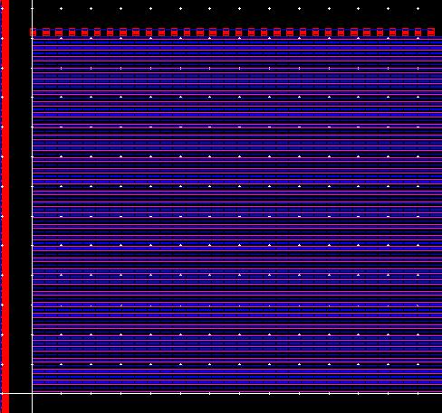
6 Block Diagram
7 Block Level Transmission gates o AND, MUXes, etc.
8 Bit Cell Level Traditional design

9 Bit Cell Level Pass Gate PDN NMOS γ = I SD = W D L A I SA L D W A I cell < I SD γ I cell > γ I SA γ+1 I cell > I SD I cell < I SA γ+1 All equations and images on this page are from Ding-Ming Kwai & IP Library Company
10 Bit Cell Level Carr D., Park J., Reyno D. High Speed Cache Powerpoint Presentation to PICo (2010) Desire: small area & stable Q Reality: only need to get below V M, don t need to get below V T We ended up with a cell ratio of 1.2 and Pull-up ratio of 1.11, following Carr et al. s (2010) successful design choices as well
11 Device Level W/L determined by sweeping and using previously mentioned ratios o o o PMOS: 180n NMOS: 240n Pass Gate: 200n Compared to previous years, industry standard, etc. o Short Answer: bigger
12 Novelties Latching Voltage Sense Amplifier Stacked Transmission Gate Decoders
13 Sense Amplifier Differential Main Idea: BL > BLB: Output = high BL < BLB: Output = low ΔV BL = I cell Δt / C BL Pros Easy to implement Dynamic Low Power ECE410 Chapter 13 Lecture at Michigan State Cons Dynamic
14 Latching Voltage Sense Amplifier Pros ~23% Faster Reads* o Therefore, ~23% smaller ΔV Low power Cons More FETs/Larger area *Based on 2011 Team 1 measurement Ryan, J. F., & Calhoun, B. H. Minimizing offset for latching voltagemode sense amplifiers for sub-threshold operation (2008)
15 Layout Note: No taps are present in the layout We attempted to optimize area as well Clutter

16 6T Cell Layout μm 2.16 μm

17 2x2 Cell Layout


18 Block Layout μm μm
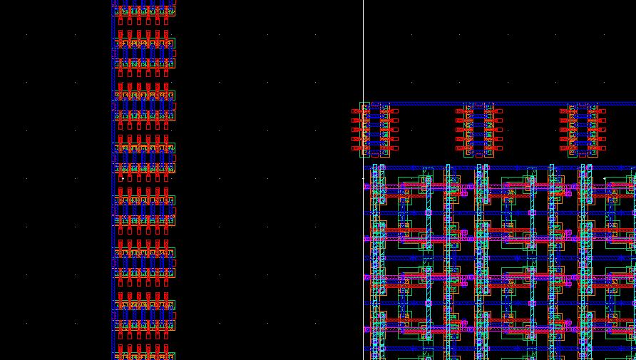
19 Block with Peripherals 69.63μm x μm

20 Sense Amp Differential Voltage Latching Sense Amplifier Messy, Cluttered

21 Transmission Gate Versatile, Used in most of the peripherals Helpful with other layouts

22 32b Decoder Layout

23 64b Decoder Layout
24 Testbench Simulation setup for SRAM Reads and Writes To emulate conditions seen in full array: Recreate worst case paths For both inputs and outputs

25 Simulation Results PRECHARGE WORDLINE READ WRITE DATA Q QB OUT
26 Metrics Metrics Our Group Comparison to Team XOR (2010) Total Metric x J s 2 mm2 W Better by 882% 1 Bitcell Area 2.3 μm 2 Worse by 130% Total Area mm 2 Worse by 22% Total Energy nj Worse by 20% Read Delay 0.54 ns Better by 63% Write Delay 0.11 ns Better by 58% Total Delay 0.54 ns Better by 63% Idle Power.0698 W Better by 41%
27 Future Refinement SKILL and OCEAN Move further on the Pareto curve Predecoding Error Correcting Code Vectorize signals Ultra-thin Layout Carr D., Park J., Reyno D. A High Speed 64kb SRAM Cache in 45nm Technology (2010)


, Team 1 (2011), and")

28 Acknowledgments Divya Akella University of Virginia Aatmesh Shrivastava, PICo liaison Dr. Benton Calhoun, PICo liaison & Team XOR (2010), Team 2 (2010), Team 1 (2011), and many others! We also acknowledge and offer good luck to Team Innovation!
29 Questions? ಠ_ಠ
30 References [All pictures are cited in their captions] Calhoun, B., Design Principles for Digital CMOS Integrated Circuits, (March 7, 2012) L. Hamouche and B. Allard, Low power options for 32nm always-on SRAM architecture, Solid State Electronics, Mann, R., and B. Calhoun, "New category of ultra-thin notchless 6T SRAM cell layout topologies for sub-22nm", ISQED, Rabaey, J., Chandrakasan A., Nikolic, B., Digital Integrated Circuits (2nd Edition), (Dec 24, 2002) Rabaey, J. Digital Integrated Circuits: A Design Perspective. Prentice Hall, Ryan, J. F., & Calhoun, B. H. Minimizing Offset for Latching Voltage Mode Sense Amplifiers for Sub-Threshold Operation. 9th International Symposium on Quality Electronic Design, Wang, A., Calhoun, B. H., & Chandrakasan, A. P. Sub-Threshold Design for Ultra Low-Power Systems. Springer, Previous Groups from ECE 4332 VLSI Design at University of Virginia (e.g. 2009, 2010, 2011, 2012)
CMPEN 411 VLSI Digital Circuits Spring Lecture 24: Peripheral Memory Circuits
 CMPEN 411 VLSI Digital Circuits Spring 2011 Lecture 24: Peripheral Memory Circuits [Adapted from Rabaey s Digital Integrated Circuits, Second Edition, 2003 J. Rabaey, A. Chandrakasan, B. Nikolic] Sp11
Lecture 8: Memory Peripherals
 Digital Integrated Circuits (83-313) Lecture 8: Memory Peripherals Semester B, 2016-17 Lecturer: Dr. Adam Teman TAs: Itamar Levi, Robert Giterman 20 May 2017 Disclaimer: This course was prepared, in its
Static Random Access Memory - SRAM Dr. Lynn Fuller Webpage:
 ROCHESTER INSTITUTE OF TECHNOLOGY MICROELECTRONIC ENGINEERING Static Random Access Memory - SRAM Dr. Lynn Fuller Webpage: http://people.rit.edu/lffeee 82 Lomb Memorial Drive Rochester, NY 14623-5604 Email:
Design and Implement of Low Power Consumption SRAM Based on Single Port Sense Amplifier in 65 nm
 Journal of Computer and Communications, 2015, 3, 164-168 Published Online November 2015 in SciRes. http://www.scirp.org/journal/jcc http://dx.doi.org/10.4236/jcc.2015.311026 Design and Implement of Low
Low Power Design of Schmitt Trigger Based SRAM Cell Using NBTI Technique
 Low Power Design of Schmitt Trigger Based SRAM Cell Using NBTI Technique M.Padmaja 1, N.V.Maheswara Rao 2 Post Graduate Scholar, Gayatri Vidya Parishad College of Engineering for Women, Affiliated to JNTU,
Effect of W/L Ratio on SRAM Cell SNM for High-Speed Application
 Effect of W/L Ratio on SRAM Cell SNM for High-Speed Application Akhilesh Goyal 1, Abhishek Tomar 2, Aman Goyal 3 1PG Scholar, Department Of Electronics and communication, SRCEM Banmore, Gwalior, India
DESIGN & IMPLEMENTATION OF SELF TIME DUMMY REPLICA TECHNIQUE IN 128X128 LOW VOLTAGE SRAM
 DESIGN & IMPLEMENTATION OF SELF TIME DUMMY REPLICA TECHNIQUE IN 128X128 LOW VOLTAGE SRAM 1 Mitali Agarwal, 2 Taru Tevatia 1 Research Scholar, 2 Associate Professor 1 Department of Electronics & Communication
Design Of A Comparator For Pipelined A/D Converter
 Design Of A Comparator For Pipelined A/D Converter Ms. Supriya Ganvir, Mr. Sheetesh Sad ABSTRACT`- This project reveals the design of a comparator for pipeline ADC. These comparator is designed using preamplifier
Analysis of SRAM Bit Cell Topologies in Submicron CMOS Technology
 Analysis of SRAM Bit Cell Topologies in Submicron CMOS Technology Vipul Bhatnagar, Pradeep Kumar and Sujata Pandey Amity School of Engineering and Technology, Amity University Uttar Pradesh, Noida, INDIA
Investigating Delay-Power Tradeoff in Kogge-Stone Adder in Standby Mode and Active Mode
 Investigating Delay-Power Tradeoff in Kogge-Stone Adder in Standby Mode and Active Mode Design Review 2, VLSI Design ECE6332 Sadredini Luonan wang November 11, 2014 1. Research In this design review, we
Memory Basics. historically defined as memory array with individual bit access refers to memory with both Read and Write capabilities
 Memory Basics RAM: Random Access Memory historically defined as memory array with individual bit access refers to memory with both Read and Write capabilities ROM: Read Only Memory no capabilities for
CHAPTER 3 NEW SLEEPY- PASS GATE
 56 CHAPTER 3 NEW SLEEPY- PASS GATE 3.1 INTRODUCTION A circuit level design technique is presented in this chapter to reduce the overall leakage power in conventional CMOS cells. The new leakage po leepy-
Announcements. Advanced Digital Integrated Circuits. Quiz #3 today Homework #4 posted This lecture until 4pm
 EE241 - Spring 2011 dvanced Digital Integrated Circuits Lecture 20: High-Performance Logic Styles nnouncements Quiz #3 today Homework #4 posted This lecture until 4pm Reading: Chapter 8 in the owhill text
Design and Implementation of High Speed Sense Amplifier for Sram
 American-Eurasian Journal of Scientific Research 12 (6): 320-326, 2017 ISSN 1818-6785 IDOSI Publications, 2017 DOI: 10.5829/idosi.aejsr.2017.320.326 Design and Implementation of High Speed Sense Amplifier
SNM Analysis of 6T SRAM at 32NM and 45NM Technique
 SNM Analysis of 6T SRAM at 32NM and 45NM Technique Anurag Dandotiya ITM Universe Gwalior Amit S. Rajput Assistant Professor ITM Universe Gwalior OBJECTIVE OF THE CHAPTER In this paper we analyze the effect
II. Previous Work. III. New 8T Adder Design
 ISSN: 2277 128X International Journal of Advanced Research in Computer Science and Software Engineering Research Paper Available online at: High Performance Circuit Level Design For Multiplier Arun Kumar
EEC 216 Lecture #10: Ultra Low Voltage and Subthreshold Circuit Design. Rajeevan Amirtharajah University of California, Davis
 EEC 216 Lecture #1: Ultra Low Voltage and Subthreshold Circuit Design Rajeevan Amirtharajah University of California, Davis Opportunities for Ultra Low Voltage Battery Operated and Mobile Systems Wireless
Jyoti Sharma 1, Rajesh Parihar 2 1 M.Tech Scholar, CBSGIs, Jhajjar
 Design and Analysis of Low Power High Speed Current Latch Sense Amplifier Jyoti Sharma 1, Rajesh Parihar 2 1 M.Tech Scholar, CBSGIs, Jhajjar 2 Asst. Professor, H.O.D., ECE/EE, CBSGIs, Jhajjar Abstract-
Read/Write Stability Improvement of 8T Sram Cell Using Schmitt Trigger
 International Journal of Scientific and Research Publications, Volume 5, Issue 2, February 2015 1 Read/Write Stability Improvement of 8T Sram Cell Using Schmitt Trigger Dr. A. Senthil Kumar *,I.Manju **,
Low Power, Area Efficient FinFET Circuit Design
 Low Power, Area Efficient FinFET Circuit Design Michael C. Wang, Princeton University Abstract FinFET, which is a double-gate field effect transistor (DGFET), is more versatile than traditional single-gate
8T-SRAM Cell with Improved Read and Write Margins in 65 nm CMOS Technology
 8T-SRAM Cell with Improved Read and Write Margins in 65 nm CMOS Technology Farshad Moradi (&), Mohammad Tohidi, Behzad Zeinali, and Jens K. Madsen Integrated Circuits and Electronics Laboratory, Department
Optimizing Design Time
 Optimizing Power @ Design Time Memory Benton H. Calhoun Jan M. Rabaey Role of Memory in ICs Memory is very important Focus in this chapter is embedded memory Percentage of area going to memory is increasing
nmos, pmos - Enhancement and depletion MOSFET, threshold voltage, body effect
 COURSE DELIVERY PLAN - THEORY Page! 1 of! 7 Department of Electronics and Communication Engineering B.E/B.Tech/M.E/M.Tech : EC Regulation: 2016(Autonomous) PG Specialization : Not Applicable Sub. Code
Low Power Realization of Subthreshold Digital Logic Circuits using Body Bias Technique
 Indian Journal of Science and Technology, Vol 9(5), DOI: 1017485/ijst/2016/v9i5/87178, Februaru 2016 ISSN (Print) : 0974-6846 ISSN (Online) : 0974-5645 Low Power Realization of Subthreshold Digital Logic
Robust Subthreshold Circuit Designing Using Sub-threshold Source Coupled Logic (STSCL)
") International Journal of Electronics Engineering, (1), 010, pp. 19-3 Robust Subthreshold Circuit Designing Using Sub-threshold Source Coupled Logic (STSCL) Ashutosh Nandi 1, Gaurav Saini, Amit Kumar Jaiswal
International Journal of Electronics Engineering, (1), 010, pp. 19-3 Robust Subthreshold Circuit Designing Using Sub-threshold Source Coupled Logic (STSCL) Ashutosh Nandi 1, Gaurav Saini, Amit Kumar Jaiswal
[Vivekanand*, 4.(12): December, 2015] ISSN: (I2OR), Publication Impact Factor: 3.785
![[Vivekanand*, 4.(12): December, 2015] ISSN: (I2OR), Publication Impact Factor: 3.785](/thumbs/84/90801833.jpg "[Vivekanand*, 4.(12): December, 2015] ISSN: (I2OR), Publication Impact Factor: 3.785") IJESRT INTERNATIONAL JOURNAL OF ENGINEERING SCIENCES & RESEARCH TECHNOLOGY DESIGN AND IMPLEMENTATION OF HIGH RELIABLE 6T SRAM CELL V.Vivekanand*, P.Aditya, P.Pavan Kumar * Electronics and Communication
IJESRT INTERNATIONAL JOURNAL OF ENGINEERING SCIENCES & RESEARCH TECHNOLOGY DESIGN AND IMPLEMENTATION OF HIGH RELIABLE 6T SRAM CELL V.Vivekanand*, P.Aditya, P.Pavan Kumar * Electronics and Communication
Lecture 6: Electronics Beyond the Logic Switches Xufeng Kou School of Information Science and Technology ShanghaiTech University
 Lecture 6: Electronics Beyond the Logic Switches Xufeng Kou School of Information Science and Technology ShanghaiTech University EE 224 Solid State Electronics II Lecture 3: Lattice and symmetry 1 Outline
SRAM based 28 nm Technology for consumer electronics applications
 IOSR Journal of VLSI and Signal Processing (IOSR-JVSP) Volume 4, Issue 2, Ver. IV (Mar-Apr. 2014), PP 38-44 e-issn: 2319 4200, p-issn No. : 2319 4197 SRAM based 28 nm Technology for consumer electronics
Cmos Full Adder and Multiplexer Based Encoder for Low Resolution Flash Adc
 IOSR Journal of Electronics and Communication Engineering (IOSR-JECE) e-issn: 2278-2834,p- ISSN: 2278-8735.Volume 12, Issue 2, Ver. II (Mar.-Apr. 2017), PP 20-27 www.iosrjournals.org Cmos Full Adder and
Analysis of Low Power-High Speed Sense Amplifier in Submicron Technology
 Voltage IJSRD - International Journal for Scientific Research & Development Vol. 2, Issue 02, 2014 ISSN (online): 2321-0613 Analysis of Low Power-High Speed Sense Amplifier in Submicron Technology Sunil
Performance Comparison of CMOS and Finfet Based Circuits At 45nm Technology Using SPICE
 RESEARCH ARTICLE OPEN ACCESS Performance Comparison of CMOS and Finfet Based Circuits At 45nm Technology Using SPICE Mugdha Sathe*, Dr. Nisha Sarwade** *(Department of Electrical Engineering, VJTI, Mumbai-19)
IMPLEMENTATION OF POWER GATING TECHNIQUE IN CMOS FULL ADDER CELL TO REDUCE LEAKAGE POWER AND GROUND BOUNCE NOISE FOR MOBILE APPLICATION
 International Journal of Electronics, Communication & Instrumentation Engineering Research and Development (IJECIERD) ISSN 2249-684X Vol.2, Issue 3 Sep 2012 97-108 TJPRC Pvt. Ltd., IMPLEMENTATION OF POWER
Reducing the Sub-threshold and Gate-tunneling Leakage of SRAM Cells using Dual-V t and Dual-T ox Assignment
 Reducing the Sub-threshold and Gate-tunneling Leakage of SRAM Cells using Dual-V t and Dual-T ox Assignment Behnam Amelifard Department of EE-Systems University of Southern California Los Angeles, CA (213)
Lecture 12 Memory Circuits. Memory Architecture: Decoders. Semiconductor Memory Classification. Array-Structured Memory Architecture RWM NVRWM ROM
 Semiconductor Memory Classification Lecture 12 Memory Circuits RWM NVRWM ROM Peter Cheung Department of Electrical & Electronic Engineering Imperial College London Reading: Weste Ch 8.3.1-8.3.2, Rabaey
EE241 - Spring 2002 Advanced Digital Integrated Circuits
 EE241 - Spring 2002 dvanced Digital Integrated Circuits Lecture 7 MOS Logic Styles nnouncements Homework #1 due 2/19 1 Reading Chapter 7 in the text by K. ernstein ackground material from Rabaey References»
Design of 32-bit ALU using Low Power Energy Efficient Full Adder Circuits
 Design of 32-bit ALU using Low Power Energy Efficient Full Adder Circuits Priyadarshini.V Department of ECE Gudlavalleru Engieering College,Gudlavalleru darshiniv708@gmail.com Ramya.P Department of ECE
SRAM Read-Assist Scheme for Low Power High Performance Applications
 SRAM Read-Assist Scheme for Low Power High Performance Applications Ali Valaee A Thesis In the Department of Electrical and Computer Engineering Presented in Partial Fulfillment of the Requirements for
Variation Aware Performance Analysis of Gain Cell Embedded DRAMs
 Variation Aware Performance Analysis of Gain Cell Embedded DRAMs Wei Zhang Department of ECE University of Minnesota Minneapolis, MN zhang78@umn.edu Ki Chul Chun Department of ECE University of Minnesota
MOS CURRENT MODE LOGIC BASED PRIORITY ENCODERS
 MOS CURRENT MODE LOGIC BASED PRIORITY ENCODERS Neeta Pandey 1, Kirti Gupta 2, Stuti Gupta 1, Suman Kumari 1 1 Dept. of Electronics and Communication, Delhi Technological University, New Delhi (India) 2
Design of Two High Performance 1-Bit CMOS Full Adder Cells
 Int. J. Com. Dig. Sys. 2, No., 47-52 (23) 47 International Journal of Computing and Digital Systems -- An International Journal @ 23 UOB CSP, University of Bahrain Design of Two High Performance -Bit CMOS
Energy Efficiency of Power-Gating in Low-Power Clocked Storage Elements
 Energy Efficiency of Power-Gating in Low-Power Clocked Storage Elements Christophe Giacomotto 1, Mandeep Singh 1, Milena Vratonjic 1, Vojin G. Oklobdzija 1 1 Advanced Computer systems Engineering Laboratory,
Opportunities and Challenges in Ultra Low Voltage CMOS. Rajeevan Amirtharajah University of California, Davis
 Opportunities and Challenges in Ultra Low Voltage CMOS Rajeevan Amirtharajah University of California, Davis Opportunities for Ultra Low Voltage Battery Operated and Mobile Systems Wireless sensors RFID
A Read-Decoupled Gated-Ground SRAM Architecture for Low-Power Embedded Memories
 A Read-Decoupled Gated-Ground SRAM Architecture for Low-Power Embedded Memories Wasim Hussain A Thesis In The Department of Electrical and Computer Engineering Presented in Partial Fulfillment of the Requirements
A High Performance IDDQ Testable Cache for Scaled CMOS Technologies
 A High Performance IDDQ Testable Cache for Scaled CMOS Technologies Swarup Bhunia, Hai Li and Kaushik Roy Purdue University, 1285 EE Building, West Lafayette, IN 4796 {bhunias, hl, kaushik}@ecn.purdue.edu
ASYNCHRONOUS RAM ADDRESS TRANSITION DETECTION CIRCUIT
 ASYNCHRONOUS RAM ADDRESS TRANSITION DETECTION CIRCUIT MR. HIMANSHU J. SHAH 1, ASST. PROF.VIRENDRASINGH TIWARI 2 1.MTech (Dc)Student,Department Of Electronics & Communication, Sagar Institute Of Research
Design and Implementation of ALU Chip using D3L Logic and Ancient Mathematics
 Design and Implementation of ALU Chip using D3L and Ancient Mathematics Mohanarangan S PG Student (M.E-Applied Electronics) Department of Electronics and Communicaiton Engineering Sri Venkateswara College
! Sequential Logic. ! Timing Hazards. ! Dynamic Logic. ! Add state elements (registers, latches) ! Compute. " From state elements
 ! Compute. From state elements") ESE 570: Digital Integrated Circuits and VLSI Fundamentals Lec 19: April 2, 2019 Sequential Logic, Timing Hazards and Dynamic Logic Lecture Outline! Sequential Logic! Timing Hazards! Dynamic Logic 4 Sequential
ESE 570: Digital Integrated Circuits and VLSI Fundamentals Lec 19: April 2, 2019 Sequential Logic, Timing Hazards and Dynamic Logic Lecture Outline! Sequential Logic! Timing Hazards! Dynamic Logic 4 Sequential
Total reduction of leakage power through combined effect of Sleep stack and variable body biasing technique
 Total reduction of leakage power through combined effect of Sleep and variable body biasing technique Anjana R 1, Ajay kumar somkuwar 2 Abstract Leakage power consumption has become a major concern for
A Novel Technique to Reduce Write Delay of SRAM Architectures
 A Novel Technique to Reduce Write Delay of SRAM Architectures SWAPNIL VATS AND R.K. CHAUHAN * Department of Electronics and Communication Engineering M.M.M. Engineering College, Gorahpur-73 010, U.P. INDIA
A Novel Radiation Tolerant SRAM Design Based on Synergetic Functional Component Separation for Nanoscale CMOS.
 A Novel Radiation Tolerant SRAM Design Based on Synergetic Functional Component Separation for Nanoscale CMOS. Abstract This paper presents a novel SRAM design for nanoscale CMOS. The new design addresses
EEC 118 Spring 2010 Lab #1: NMOS and PMOS Transistor Parameters
 EEC 118 Spring 2010 Lab #1: NMOS and PMOS Transistor Parameters Dept. of Electrical and Computer Engineering University of California, Davis March 18, 2010 Reading: Rabaey Chapter 3 [1]. Reference: Kang
SUB-THRESHOLD digital circuit design has emerged as
 IEEE JOURNAL OF SOLID-STATE CIRCUITS, VOL. 41, NO. 7, JULY 2006 1673 Static Noise Margin Variation for Sub-threshold SRAM in 65-nm CMOS Benton H. Calhoun, Member, IEEE, and Anantha P. Chandrakasan, Fellow,
Performance of Low Power SRAM Cells On SNM and Power Dissipation
 Performance of Low Power SRAM Cells On SNM and Power Dissipation Kanika Kaur 1, Anurag Arora 2 KIIT College of Engineering, Gurgaon, Haryana, INDIA Abstract: Over the years, power requirement reduction
Lecture 4&5 CMOS Circuits
 Lecture 4&5 CMOS Circuits Xuan Silvia Zhang Washington University in St. Louis http://classes.engineering.wustl.edu/ese566/ Worst-Case V OL 2 3 Outline Combinational Logic (Delay Analysis) Sequential Circuits
Design of a high speed and low power Sense Amplifier
 Design of a high speed and low power Sense Amplifier A dissertation submitted in partial fulfillment of the requirement for the award of degree of Master of Technology in VLSI Design & CAD Submitted by
SRAM Read Performance Degradation under Asymmetric NBTI and PBTI Stress: Characterization Vehicle and Statistical Aging
 SRAM Read Performance Degradation under Asymmetric NBTI and PBTI Stress: Characterization Vehicle and Statistical Aging Xiaofei Wang,2 Weichao Xu 2 and Chris H. Kim 2 Intel Corporation, Hillsboro 2 University
Performance analysis of Modified SRAM Memory Design using leakage power reduction
 Performance analysis of Modified Memory Design using leakage power reduction 1 Udaya Bhaskar Pragada, 2 J.S.S. Rama Raju, 3 Mahesh Gudivaka 1 PG Student, 2 Associate Professor, 3 Assistant Professor 1
UMAINE ECE Morse Code ROM and Transmitter at ISM Band Frequency
 UMAINE ECE Morse Code ROM and Transmitter at ISM Band Frequency Jamie E. Reinhold December 15, 2011 Abstract The design, simulation and layout of a UMAINE ECE Morse code Read Only Memory and transmitter
Implementation of Carry Select Adder using CMOS Full Adder
 Implementation of Carry Select Adder using CMOS Full Adder Smitashree.Mohapatra Assistant professor,ece department MVSR Engineering College Nadergul,Hyderabad-510501 R. VaibhavKumar PG Scholar, ECE department(es&vlsid)
Variability-Aware Design of Static Random Access Memory Bit-Cell
 Variability-Aware Design of Static Random Access Memory Bit-Cell by Vasudha Gupta A thesis presented to the University of Waterloo in fulfilment of the thesis requirement for the degree of Master of Applied
Subthreshold SRAM Design for Energy Efficient Applications in Nanometric CMOS Technologies
 Subthreshold SRAM Design for Energy Efficient Applications in Nanometric CMOS Technologies by Morteza Nabavi A thesis presented to the University of Waterloo in fulfillment of the thesis requirement for
A gate sizing and transistor fingering strategy for
 LETTER IEICE Electronics Express, Vol.9, No.19, 1550 1555 A gate sizing and transistor fingering strategy for subthreshold CMOS circuits Morteza Nabavi a) and Maitham Shams b) Department of Electronics,
International Journal of Scientific & Engineering Research, Volume 4, Issue 5, May ISSN
 International Journal of Scientific & Engineering Research, Volume 4, Issue 5, May-2013 2190 Biquad Infinite Impulse Response Filter Using High Efficiency Charge Recovery Logic K.Surya 1, K.Chinnusamy
A Low-Power SRAM Design Using Quiet-Bitline Architecture
 A Low-Power SRAM Design Using uiet-bitline Architecture Shin-Pao Cheng Shi-Yu Huang Electrical Engineering Department National Tsing-Hua University, Taiwan Abstract This paper presents a low-power SRAM
Charge recycling 8T SRAM design for low voltage robust operation
 Southern Illinois University Carbondale OpenSIUC Articles Department of Electrical and Computer Engineering Spring --0 Charge recycling T SRAM design for low voltage robust operation Xu Wang Shanghai Jiaotong
Digital Timing Control in SRAMs for Yield Enhancement and Graceful Aging Degradation
 Digital Timing Control in SRAMs for Yield Enhancement and Graceful Aging Degradation by Adam Neale A thesis presented to the University of Waterloo in fulfillment of the thesis requirement for the degree
Current Mode Sense Amplifiers Design in 0.25um CMOS Technology
 Current Mode Design in.5um CMOS Technology A. CHRISANTHOPOULOS 1, Y. MOISIADIS, Y. TSIATOUHAS 1, G. KAMOULAKOS 1 1 ISD S.A. K.Varnali Str., 15 33 Halandri, Athens GREECE University of Athens Department
A DUAL-EDGED TRIGGERED EXPLICIT-PULSED LEVEL CONVERTING FLIP-FLOP WITH A WIDE OPERATION RANGE
 A DUAL-EDGED TRIGGERED EXPLICIT-PULSED LEVEL CONVERTING FLIP-FLOP WITH A WIDE OPERATION RANGE Mei-Wei Chen 1, Ming-Hung Chang 1, Pei-Chen Wu 1, Yi-Ping Kuo 1, Chun-Lin Yang 1, Yuan-Hua Chu 2, and Wei Hwang
Intellect Amplifier, Current Clasped and Filled Current Approach Sense Amplifiers Techniques Based Low Power SRAM
 Intellect Amplifier, Current Clasped and Filled Current Approach Sense Amplifiers Techniques Based Low Power SRAM V. Karthikeyan 1 1 Department of ECE, SVSCE, Coimbatore, Tamilnadu, India, Karthick77keyan@gmail.com
Variability in Sub-100nm SRAM Designs
 Variability in Sub-100nm SRAM Designs Ray Heald & Ping Wang Sun Microsystems Ray Heald & Ping Wang ICCAD 2004 Variability in Sub-100nm SRAM Designs 11/9/04 1 Outline Background: Quick review of what is
電子電路. Memory and Advanced Digital Circuits
 電子電路 Memory and Advanced Digital Circuits Hsun-Hsiang Chen ( 陳勛祥 ) Department of Electronic Engineering National Changhua University of Education Email: chenhh@cc.ncue.edu.tw Spring 2010 2 Reference Microelectronic
Duty-Cycle Shift under Asymmetric BTI Aging: A Simple Characterization Method and its Application to SRAM Timing
 Duty-Cycle Shift under Asymmetric BTI Aging: A Simple Characterization Method and its Application to SRAM Timing 1 Xiaofei Wang, 2 John Keane, 2 Pulkit Jain, 3 Vijay Reddy and 1 Chris H. Kim 1 University
ECEN 720 High-Speed Links: Circuits and Systems
 1 ECEN 720 High-Speed Links: Circuits and Systems Lab4 Receiver Circuits Objective To learn fundamentals of receiver circuits. Introduction Receivers are used to recover the data stream transmitted by
Circuit and CAD Techniques for Expanding the SRAM Design Space
 Circuit and CAD Techniques for Expanding the SRAM Design Space James Boley Department of Electrical and Computer Engineering University of Virginia A Dissertation Proposal Presented in Partial Fulfillment
Memory (Part 1) RAM memory
 RAM memory") Budapest University of Technology and Economics Department of Electron Devices Technology of IT Devices Lecture 7 Memory (Part 1) RAM memory Semiconductor memory Memory Overview MOS transistor recap and
Budapest University of Technology and Economics Department of Electron Devices Technology of IT Devices Lecture 7 Memory (Part 1) RAM memory Semiconductor memory Memory Overview MOS transistor recap and
Ultra-low voltage high-speed Schmitt trigger circuit in SOI MOSFET technology
 Ultra-low voltage high-speed Schmitt trigger circuit in SOI MOSFET technology Kyung Ki Kim a) and Yong-Bin Kim b) Department of Electrical and Computer Engineering, Northeastern University, Boston, MA
Design and analysis of 6T SRAM cell using FINFET at Nanometer Regime Monali S. Mhaske 1, Prof. S. A. Shaikh 2
 Design and analysis of 6T SRAM cell using FINFET at Nanometer Regime Monali S. Mhaske 1, Prof. S. A. Shaikh 2 1 ME, Dept. Of Electronics And Telecommunication,PREC, Maharashtra, India 2 Associate Professor,
Leakage Power Reduction for Logic Circuits Using Variable Body Biasing Technique
 Leakage Power Reduction for Logic Circuits Using Variable Body Biasing Technique Anjana R 1 and Ajay K Somkuwar 2 Assistant Professor, Department of Electronics and Communication, Dr. K.N. Modi University,
Minimizing the Sub Threshold Leakage for High Performance CMOS Circuits Using Stacked Sleep Technique
 International Journal of Electrical Engineering. ISSN 0974-2158 Volume 10, Number 3 (2017), pp. 323-335 International Research Publication House http://www.irphouse.com Minimizing the Sub Threshold Leakage
Ultra Low Voltage Operation with Bootstrap Scheme for Single Power Supply SOI-SRAM
 [ 2007 International Conference on VLSI Design ] Jan. 9, 2007 Ultra Low Voltage Operation with Bootstrap Scheme for Single Power Supply SOI-SRAM Masaaki Iijima, Masayuki Kitamura, Masahiro Numa, *Akira
LOW POWER HIGH PERFORMANCE DECODER USING SWITCH LOGIC S. HAMEEDA NOOR 1, T.VIJAYA NIRMALA 2, M.V.SUBBAIAH 3 S.SALEEM 4
 RESEARCH ARTICLE OPEN ACCESS LOW POWER HIGH PERFORMANCE DECODER USING SWITCH LOGIC S. HAMEEDA NOOR 1, T.VIJAYA NIRMALA 2, M.V.SUBBAIAH 3 S.SALEEM 4 Abstract: This document introduces a switch design method
International Journal of Engineering Trends and Technology (IJETT) Volume 45 Number 5 - March 2017
 Volume 45 Number 5 - March 2017") Performance Evaluation in Adiabatic Logic Circuits for Low Power VLSI Design Tabassum Ara #1, Amrita Khera #2, # PG Student [VLSI], Dept. of ECE, Trinity stitute of Technology and Research, Bhopal, RGPV
Performance Evaluation in Adiabatic Logic Circuits for Low Power VLSI Design Tabassum Ara #1, Amrita Khera #2, # PG Student [VLSI], Dept. of ECE, Trinity stitute of Technology and Research, Bhopal, RGPV
Study of SRAM Cell for Balancing Read and Write Margins in Sub-100nm Technology using Noise-Curve Method
 Study of SRAM Cell for Balancing Read and Write Margins in Sub-100nm Technology using Noise-Curve Method Malleshaiah G. V Department of Electronics and Communication Engineering, Eastpoint College of Engineering
Design of Low Power High Speed Fully Dynamic CMOS Latched Comparator
 International Journal of Engineering Research and Development e-issn: 2278-067X, p-issn: 2278-800X, www.ijerd.com Volume 10, Issue 4 (April 2014), PP.01-06 Design of Low Power High Speed Fully Dynamic
Comparison of High Speed & Low Power Techniques GDI & McCMOS in Full Adder Design
 International Conference on Multidisciplinary Research & Practice P a g e 625 Comparison of High Speed & Low Power Techniques & in Full Adder Design Shikha Sharma 1, ECE, Geetanjali Institute of Technical
[Singh*, 5(3): March, 2016] ISSN: (I2OR), Publication Impact Factor: 3.785
![[Singh*, 5(3): March, 2016] ISSN: (I2OR), Publication Impact Factor: 3.785](/thumbs/85/92290485.jpg "[Singh*, 5(3): March, 2016] ISSN: (I2OR), Publication Impact Factor: 3.785") IJESRT INTERNATIONAL JOURNAL OF ENGINEERING SCIENCES & RESEARCH TECHNOLOGY COMPARISON OF GDI BASED D FLIP FLOP CIRCUITS USING 90NM AND 180NM TECHNOLOGY Gurwinder Singh*, Ramanjeet Singh ECE Department,
IJESRT INTERNATIONAL JOURNAL OF ENGINEERING SCIENCES & RESEARCH TECHNOLOGY COMPARISON OF GDI BASED D FLIP FLOP CIRCUITS USING 90NM AND 180NM TECHNOLOGY Gurwinder Singh*, Ramanjeet Singh ECE Department,
Introduction to CMOS VLSI Design (E158) Lecture 5: Logic
 Lecture 5: Logic") Harris Introduction to CMOS VLSI Design (E158) Lecture 5: Logic David Harris Harvey Mudd College David_Harris@hmc.edu Based on EE271 developed by Mark Horowitz, Stanford University MAH E158 Lecture 5 1
Harris Introduction to CMOS VLSI Design (E158) Lecture 5: Logic David Harris Harvey Mudd College David_Harris@hmc.edu Based on EE271 developed by Mark Horowitz, Stanford University MAH E158 Lecture 5 1
Power-Area trade-off for Different CMOS Design Technologies
 Power-Area trade-off for Different CMOS Design Technologies Priyadarshini.V Department of ECE Sri Vishnu Engineering College for Women, Bhimavaram dpriya69@gmail.com Prof.G.R.L.V.N.Srinivasa Raju Head
Near-threshold Computing of Single-rail MOS Current Mode Logic Circuits
 Research Journal of Applied Sciences, Engineering and Technology 5(10): 2991-2996, 2013 ISSN: 2040-7459; e-issn: 2040-7467 Maxwell Scientific Organization, 2013 Submitted: September 16, 2012 Accepted:
A NEW APPROACH TO DESIGN LOW POWER CMOS FLASH A/D CONVERTER
 A NEW APPROACH TO DESIGN LOW POWER CMOS FLASH A/D CONVERTER C Mohan¹ and T Ravisekhar 2 ¹M. Tech (VLSI) Student, Sree Vidyanikethan Engineering College (Autonomous), Tirupati, India 2 Assistant Professor,
EEC 118 Lecture #12: Dynamic Logic
 EEC 118 Lecture #12: Dynamic Logic Rajeevan Amirtharajah University of California, Davis Jeff Parkhurst Intel Corporation Outline Today: Alternative MOS Logic Styles Dynamic MOS Logic Circuits: Rabaey
(12) United States Patent (10) Patent No.: US 8,536,898 B2
 United States Patent (10) Patent No.: US 8,536,898 B2") US008536898B2 (12) United States Patent (10) Patent No.: US 8,536,898 B2 Rennie et al. (45) Date of Patent: Sep. 17, 2013 (54) SRAM SENSE AMPLIFIER 5,550,777 A * 8/1996 Tran... 365,205 5,627,789 A 5, 1997
US008536898B2 (12) United States Patent (10) Patent No.: US 8,536,898 B2 Rennie et al. (45) Date of Patent: Sep. 17, 2013 (54) SRAM SENSE AMPLIFIER 5,550,777 A * 8/1996 Tran... 365,205 5,627,789 A 5, 1997
Design and Analysis of Hybrid Current/Voltage CMOS SRAM Sense Amplifier with Offset Cancellation Karishma Bajaj 1, Manjit Kaur 2, Gurmohan Singh 3 1
 American International Journal of Research in Science, Technology, Engineering & Mathematics Available online at http://www.iasir.net ISSN (Print): 2328-3491, ISSN (Online): 2328-3580, ISSN (CD-ROM): 2328-3629
High Speed Communication Circuits and Systems Lecture 14 High Speed Frequency Dividers
 High Speed Communication Circuits and Systems Lecture 14 High Speed Frequency Dividers Michael H. Perrott March 19, 2004 Copyright 2004 by Michael H. Perrott All rights reserved. 1 High Speed Frequency
Duty-Cycle Shift under Asymmetric BTI Aging: A Simple Characterization Method and its Application to SRAM Timing 1 Xiaofei Wang
 Duty-Cycle Shift under Asymmetric BTI Aging: A Simple Characterization Method and its Application to SRAM Timing 1 Xiaofei Wang Abstract the effect of DC BTI stress on the clock signal's dutycycle has
A Survey of the Low Power Design Techniques at the Circuit Level
 A Survey of the Low Power Design Techniques at the Circuit Level Hari Krishna B Assistant Professor, Department of Electronics and Communication Engineering, Vagdevi Engineering College, Warangal, India
IJSRD - International Journal for Scientific Research & Development Vol. 4, Issue 02, 2016 ISSN (online):
:") IJSRD - International Journal for Scientific Research & Development Vol. 4, Issue 02, 2016 ISSN (online): 2321-0613 Design & Analysis of CMOS Telescopic Operational Transconductance Amplifier (OTA) with
IJSRD - International Journal for Scientific Research & Development Vol. 4, Issue 02, 2016 ISSN (online): 2321-0613 Design & Analysis of CMOS Telescopic Operational Transconductance Amplifier (OTA) with
Combinational Logic Gates in CMOS
 Combinational Logic Gates in CMOS References: dapted from: Digital Integrated Circuits: Design Perspective, J. Rabaey UC Principles of CMOS VLSI Design: Systems Perspective, 2nd Ed., N. H. E. Weste and
STUDY OF VOLTAGE AND CURRENT SENSE AMPLIFIER
 STUDY OF VOLTAGE AND CURRENT SENSE AMPLIFIER Sandeep kumar 1, Charanjeet Singh 2 1,2 ECE Department, DCRUST Murthal, Haryana Abstract Performance of sense amplifier has considerable impact on the speed
CONTROLLING STATIC POWER LEAKAGE IN 7T SRAM CELL USING POWER GATING TECHNIQUE
 CONTROLLING STATIC POWER LEAKAGE IN 7T SRAM CELL USING POWER GATING TECHNIQUE Mr.T.Mani 1, P.Praveen 2, P.Soundararajan 3, M.Suresh 4, D.Prakash 5 1 (Assistant professor, Department of ECE, Jay shriram