Bipolar Junction Transistor (BJT)
|
|
|
- Thomasine Fleming
- 5 years ago
- Views:
Transcription
1 Bipolar Junction Transistor (BJT) 1
2 Objectives To understand the structure of BJT. To explain and analyze the basic transistor circuits. To use transistors as an amplifier and electronic switch. To design the simple circuits using transistors. To study transistor parameters from datasheet. 2


3 What is Transistor? Invented in 1947 by John Bardeen, Walter Brattain and William Shockley Hugh revolution in field of electronics First solid-state device able to amplify electric signal Universally used is Bipolar Junction Transistor(BJT) Transistor in
, there are three layers and two")
4 Transistor Structure With diodes there is one p-n junction. With bipolar junction transistors (BJT), there are three layers and two p-n junctions.. 4

5 Conducting Current Direction 5


6 Basic Functions Signal Amplifier Electronic Switch 2 Types 6
7 Basic Operation Look at this one circuit as two separate circuits, the base-emitter(left side) circuit and the collector-emitter(right side) circuit. Note that the emitter leg serves as a conductor for both circuits. The amount of current flow in the base-emitter circuit controls the amount of current that flows in the collector circuit. Small changes in base-emitter current yields a large change in collector-current. 7
8 Transistor Characteristics and Parameters As previously discussed, base-emitter current changes yield large changes in collectoremitter current. The factor of this change is called beta(β). β = I C /I B Common Emitter Configuration The beta for a transistor is not always constant. Temperature and collector current both affect beta, not to mention the normal inconsistencies during the manufacture of the transistor. There are also maximum power ratings to consider. The data sheet provides information on these characteristics. 8
9 For proper operation, the base-emitter junction is forward-biased by V BB and conducts just like a diode. The collector-base junction is reverse biased by V CC and blocks current flow through it s junction just like a diode. Remember that current flow through the base-emitter junction will help establish the path for current flow from the collector to emitter. B-C Reverse biased B-E Forward biased 9
10 There are three key dc voltages and three key dc currents to be considered. Note that these measurements are important for troubleshooting. I B : dc base current I E : dc emitter current I C : dc collector current V BE : dc voltage across base-emitter junction V CB : dc voltage across collector-base junction V CE : dc voltage from collector to emitter 10
11 Analysis of this transistor circuit to predict the dc voltages and currents requires use of Ohm s law, Kirchhoff s voltage law and the beta for the transistor. Application of these laws begins with the base circuit to determine the amount of base current. Using Kirchhoff s voltage law, subtract the.7 V BE and the remaining voltage is dropped across R B. Determining the current for the base with this information is a matter of applying of Ohm s law. I B = V RB /R B The collector current is determined by multiplying the base current by beta. What we ultimately determine by use of Kirchhoff s voltage law for series circuits is that in the base circuit V BB is distributed across the base-emitter junction and R B in the base circuit. In the collector circuit we determine that V CC is distributed proportionally across R C and the transistor(v CE ). Note. V BE = 0.7 will be used in most analysis examples. 11
12 Collector characteristic curves give a graphical illustration of the relationship of collector current and V CE with specified amounts of base current. With greater increases of V CC, V CE continues to increase until it reaches breakdown, but the current remains about the same in the linear region from.7v to the breakdown voltage.
13 Transistor regions Flat I B V CE increased, I c increased until B Curve shown for one fixed base current (I B ) 13

14 Transistor Breakdown Voltage The breakdown voltage ratings of a transistor are the maximum voltages that a transistor can handle for each of its 3 junctions. If voltages are fed to the transistor exceeding this rating, the transistor can be destroyed. A datasheet for a transistor lists the breakdown voltage ratings for the emitter-base, collector-base, and collector-emitter junctions. For example, a 2N3904 small signal transistor has the following breakdown voltage ratings: V CBO =60Vdc V CEO =40Vdc V EBO =6Vdc The first 2 letters in the subscript indicate the two transistor terminals for which the voltage rating applies, and the third letter is in reference to the third unmentioned terminal which is left open. The first voltage, V CBO indicates the maximum allowable collector-to-base voltage with the emitter open. The second voltage, V CEO is the maximum allowable collector-emitter voltage with the base open. The voltage rating, V EBO is the maximum allowable emitter-base voltage with the collector open. Exceeding any of these voltages can destroy the transistor. Ref: 14
15 Example Sketch the transistor characteristic curve for I B =5 ua to 25 ua with 5 ua increment Assume V CE does not exceed breakdown. 15
16 17
17 Cut-off Mode With no I B the transistor is in the cutoff region and just as the name implies there is practically no current flow in the collector part of the circuit. This results in only an extremely small leakage current(i CEO ) in the collector circuit. With the transistor in a cutoff state the full V CC can be measured across the collector and emitter(v CE ). 18
18 Saturation Mode Current flow in the collector part of the circuit is, as stated previously, determined by I B multiplied by β. However, there is a limit to how much current can flow in the collector circuit regardless of additional increases in I B. Once this maximum is reached, the transistor is said to be in saturation. Note that saturation can be determined by application of Ohm s law, I C(sat) =(V CC - V CE ) /R C. For Ideal case, the measured voltage across the now shorted collector and emitter(v CE ) is 0V. The practical value is around 0.2V In saturation, an increase of base current has no effect on collector circuit and the relationship I C =β.i B is no longer valid. Figure. Saturation: As I B increases due to increasing V BB, I C also increases and V CE decreases due to the increased voltage drop across R C. When the transistor reaches saturation, I C can increase no further regardless of further increase in I B. 19
19 Example Determine whether or not the transistor is in saturation. Assume V CE(sat) =0.2V and V BE(ON) =0.7V. 20
20 Example From a given circuit, determine I B,I C,I E,V BE,V CE and V CB. The transistor has a β DC =150. Assume V BE(ON) =0.7V and V CE(sat) =0.2V. 21
21 Transistor as Amplifier Amplification of a relatively small ac voltage can be had by placing the ac signal source in the base circuit. Recall that small changes in the base current circuit causes large changes in collector current circuit. The small ac voltage causes the base current to increase and decrease accordingly and with this small change in current the collector current will mimic the input only with greater amplitude. 22
22 Transistor as (Electronic)Switch A transistor when used as a switch is simply being biased so that it is in cutoff (switched off) or saturation (switched on). Remember that the V CE in cutoff is V CC and 0 V in saturation. 23

23 Electronic Switch Electronic switch uses electrical control signal for operation. The electronic switch does not contain mechanical contacts but semiconductor devices such as bipolar junction transistors or field-effect transistors. For the design, input voltage should be selected such that the output is either completely off, or completely on i.e transistor works in saturation mode. A A R on I = C I B β dc Control voltage Control voltage B Switch is open B Switch is closed I C sat = [ V V sat] CC R L CE 24
24 Application (as electronic switch) The LED in a given circuit requires 30mA to emit a sufficient light. Determine the amplitude of square wave necessary to make sure the LED emit sufficient Light. Use double the minimum value of base current as a safety margin to ensure saturation. V CC =9V,V CE(SAT) =0.3V, R C =220Ω, R B =3.3kΩ, β DC = 50, and V LED =1.6V. 25
25 Application (driving relay) From a relay driving circuit below, assume relay coil resistance = 250 Ohms, V DC = 12 V, DC current gain of transistor = 100 and V CE(SAT) = 0.1 V. V in is 0-5 V. If this relay requires 40 ma for operation, calculate R B. coil +V DC Relay NC C AC bulb NO V in R B AC 26
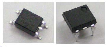
26 Plastic cases for general-purpose/small-signal transistors. 27
27
28 Example Find beta or h FE or dc current gain = 29
29 Example Refer to the datasheet. Determine whether or not the transistor is saturated in each circuit based on the maximum specific value of h FE. 30
30
31 Hint for h FE Selection The datasheet shows that the h FE can not be specified precisely by the manufacturer, because it varies very much between transistors and with electrical and thermal conditions. However, it is possible to get an approximated value. Students can start with the roughly calculation of I c. For example, if I c =20mA, we can take an intermediate value between the h FE for I c =2mA (500) and the h FE for I c =100mA (400), so let's take h FE =
32 Example Determine I B,I C,I E and β DC. 33
33 Example Find V CE,V BE,V CB in both circuits. 34

34 Testing Transistors Testing a transistor can be viewed more simply if you view it as testing two diode junctions. Forward bias having low resistance and reverse bias having infinite resistance. 35

35 The diode test function of a multimeter is more reliable than using an ohmmeter. Make sure to note whether it is an npn or pnp and polarize the test leads accordingly. In addition to the traditional DMMs there are also transistor testers. Some of these have the ability to test other parameters of the transistor, such as leakage and gain. Curve tracers give us even more detailed information about a transistors characteristics. 36
36 Conclusions The bipolar junction transistor (BJT) is constructed of three regions: base, collector, and emitter. The BJT has two pn junctions, the base-emitter junction and the base-collector junction. The two types of transistors are pnp and npn. For the BJT to operate as an amplifier, the base-emitter junction is forward-biased and the collector-base junction is reverse-biased. Of the three currents I B is very small in comparison to I E and I C. Beta is the current gain of a transistor. This the ratio of I C /I B. A transistor can be operated as an electronics switch. When the transistor is off it is in cutoff condition (no current). When the transistor is on, it is in saturation condition (maximum current). Beta can vary with temperature and also varies from transistor to transistor. 37
37 Supplement 38


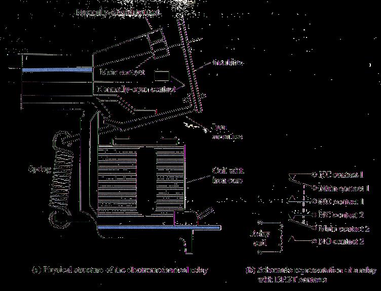
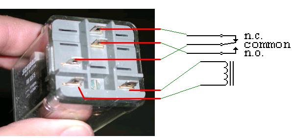
38 Relays A relay is an electrically operated switch. Current flowing through the coil of the relay creates a magnetic field which attracts a lever and changes the switch contacts. The coil current can be on or off so relays have two switch positions and they are double throw (changeover) switches. Symbol SPDT Relays DPDT Relays 39

39 40


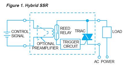
40 Solid State Relays(SSRs) Solid state relay (SSR) is a solid state electronic component that provides a similar function to an electromechanical relay but does not have any moving components, increasing long-term reliability. have become commercially available. The types of SSR are photo-coupled SSR, transformer-coupled SSR, and hybrid SSR. A photo-coupled SSR is controlled by a low voltage signal which is isolated optically from the load. The control signal in a photo-coupled SSR typically energizes an LED which activates a photo-sensitive diode. The diode turns on switching devices i.e. a back-to-back thyristor, silicon controlled rectifier, or MOSFET transistor to power on the load. Control input can be AC,DC, 4-20 ma, etc Adv: fast, smaller,lifetime Disadv: false triggering, expensive 41
41
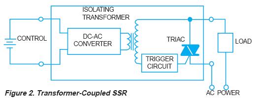
42 Isolated drive circuit For a safety consideration, an isolation between control circuit(low voltage, i.e. 5V triggering pulse) and power circuit(high voltage, i.e. 220V-few kv power plant) is very necessary. The isolation circuit prevents a damage of expensive devices used in control part. The isolation circuit can be implemented by Optoisolator and Transformer. Power Circuit Control Circuit Optocoupler/Optoisolator 43

43 Optocoupler 44
44 Example Note: This opto-isolator/driver should not be used to drive a load directly. It is intended to be a trigger for power device. Snubber Circuit Limit I F (LED input current) For Sensitive gate(optional) Snubber Circuit 45
ชาว ศวกรรมคอมพ วเตอร คณะว ศวกรรมศาสตร มหาว ทยาล ยเทคโนโลย ราชมงคลพระนคร
 EN2042102 วงจรไฟฟ าและอ เล กทรอน กส Circuits and Electronics บทท 7 ทรานซ สเตอร Bipolar Junction Transistor สาขาว ชาว ศวกรรมคอมพ วเตอร คณะว ศวกรรมศาสตร มหาว ทยาล ยเทคโนโลย ราชมงคลพระนคร Objectives Describe
Chapter 3: Bipolar Junction Transistors
 Chapter 3: Bipolar Junction Transistors Transistor Construction There are two types of transistors: pnp npn pnp The terminals are labeled: E - Emitter B - Base C - Collector npn 2 Transistor Operation
EXPERIMENT 5 CURRENT AND VOLTAGE CHARACTERISTICS OF BJT
 EXPERIMENT 5 CURRENT AND VOLTAGE CHARACTERISTICS OF BJT 1. OBJECTIVES 1.1 To practice how to test NPN and PNP transistors using multimeter. 1.2 To demonstrate the relationship between collector current
ET215 Devices I Unit 4A
 ITT Technical Institute ET215 Devices I Unit 4A Chapter 3, Section 3.1-3.2 This unit is divided into two parts; Unit 4A and Unit 4B Chapter 3 Section 3.1 Structure of Bipolar Junction Transistors The basic
ITT Technical Institute. ET215 Devices 1. Unit 6 Chapter 3, Sections
 ITT Technical Institute ET215 Devices 1 Unit 6 Chapter 3, Sections 3.7-3.9 Chapter 3 Section 3.7 The Bipolar Transistor as a Switch Objectives: Explain how a transistor can be used as a switch 1. Compute
BFF1303: ELECTRICAL / ELECTRONICS ENGINEERING. Analog Electronics: Bipolar Junction Transistors
 BFF1303: ELECTRICAL / ELECTRONICS ENGINEERING Analog Electronics: Bipolar Junction Transistors Ismail Mohd Khairuddin, Zulkifil Md Yusof Faculty of Manufacturing Engineering Universiti Malaysia Pahang
KOM2751 Analog Electronics :: Dr. Muharrem Mercimek :: YTU - Control and Automation Dept. 1 2 (CONT D - II) DIODE APPLICATIONS
 DIODE APPLICATIONS") KOM2751 Analog Electronics :: Dr. Muharrem Mercimek :: YTU - Control and Automation Dept. 1 2 (CONT D - II) DIODE APPLICATIONS Most of the content is from the textbook: Electronic devices and circuit theory,
KOM2751 Analog Electronics :: Dr. Muharrem Mercimek :: YTU - Control and Automation Dept. 1 2 (CONT D - II) DIODE APPLICATIONS Most of the content is from the textbook: Electronic devices and circuit theory,
Chapter 4 DC Biasing BJTs. BJTs
 hapter 4 D Biasing BJTs BJTs Biasing Biasing: The D voltages applied to a transistor in order to turn it on so that it can amplify the A signal. Operating Point The D input establishes an operating or
Lecture 24: Bipolar Junction Transistors (1) Bipolar Junction Structure, Operating Regions, Biasing
 Bipolar Junction Structure, Operating Regions, Biasing") Lecture 24: Bipolar Junction Transistors (1) Bipolar Junction Structure, Operating Regions, Biasing BJT Structure the BJT is formed by doping three semiconductor regions (emitter, base, and collector)
Lecture 24: Bipolar Junction Transistors (1) Bipolar Junction Structure, Operating Regions, Biasing BJT Structure the BJT is formed by doping three semiconductor regions (emitter, base, and collector)
ELEC 2210 EXPERIMENT 7 The Bipolar Junction Transistor (BJT)
") ELEC 2210 EXPERIMENT 7 The Bipolar Junction Transistor (BJT) Objectives: The experiments in this laboratory exercise will provide an introduction to the BJT. You will use the Bit Bucket breadboarding system
ELEC 2210 EXPERIMENT 7 The Bipolar Junction Transistor (BJT) Objectives: The experiments in this laboratory exercise will provide an introduction to the BJT. You will use the Bit Bucket breadboarding system
Electronics II Lecture 2(a): Bipolar Junction Transistors
: Bipolar Junction Transistors") Lecture 2(a): Bipolar Junction Transistors A/Lectr. Khalid Shakir Dept. Of Engineering Engineering by Pearson Transistor! Transistor=Transfer+Resistor. When Transistor operates in active region its input
Lecture 2(a): Bipolar Junction Transistors A/Lectr. Khalid Shakir Dept. Of Engineering Engineering by Pearson Transistor! Transistor=Transfer+Resistor. When Transistor operates in active region its input
Chapter 3 Bipolar Junction Transistors (BJT)
") Chapter 3 Bipolar Junction Transistors (BJT) Transistors In analog circuits, transistors are used in amplifiers and linear regulated power supplies. In digital circuits they function as electrical switches,
Chapter 3 Bipolar Junction Transistors (BJT) Transistors In analog circuits, transistors are used in amplifiers and linear regulated power supplies. In digital circuits they function as electrical switches,
Lecture 3: Transistors
 Lecture 3: Transistors Now that we know about diodes, let s put two of them together, as follows: collector base emitter n p n moderately doped lightly doped, and very thin heavily doped At first glance,
Transistors and Applications
 Chapter 17 Transistors and Applications DC Operation of Bipolar Junction Transistors (BJTs) The bipolar junction transistor (BJT) is constructed with three doped semiconductor regions separated by two
Chapter 3-2 Semiconductor devices Transistors and Amplifiers-BJT Department of Mechanical Engineering
 MEMS1082 Chapter 3-2 Semiconductor devices Transistors and Amplifiers-BJT Bipolar Transistor Construction npn BJT Transistor Structure npn BJT I = I + E C I B V V BE CE = V = V B C V V E E Base-to-emitter
Analog Electronics. Electronic Devices, 9th edition Thomas L. Floyd Pearson Education. Upper Saddle River, NJ, All rights reserved.
 Analog Electronics BJT Structure The BJT has three regions called the emitter, base, and collector. Between the regions are junctions as indicated. The base is a thin lightly doped region compared to the
ECE 334: Electronic Circuits Lecture 2: BJT Large Signal Model
 Faculty of Engineering ECE 334: Electronic Circuits Lecture 2: BJT Large Signal Model Agenda I & V Notations BJT Devices & Symbols BJT Large Signal Model 2 I, V Notations (1) It is critical to understand
Chapter 6 DIFFERENT TYPES OF LOGIC GATES
 Chapter 6 DIFFERENT TYPES OF LOGIC GATES Lesson 3 RTL and DTL Gates Ch06L3-"Digital Principles and Design", Raj Kamal, Pearson Education, 2006 2 Outline Resistor transistor logic (RTL) RTL Circuit Characteristics
Concepts to be Covered
 Introductory Medical Device Prototyping Analog Circuits Part 2 Semiconductors, http://saliterman.umn.edu/ Department of Biomedical Engineering, University of Minnesota Concepts to be Covered Semiconductors
CHAPTER 3: BIPOLAR JUNCION TRANSISTOR DR. PHẠM NGUYỄN THANH LOAN
 CHAPTER 3: BIPOLAR JUNCION TRANSISTOR DR. PHẠM NGUYỄN THANH LOAN Hanoi, 9/24/2012 Contents 2 Structure and operation of BJT Different configurations of BJT Characteristic curves DC biasing method and analysis
Tutorial 2 BJTs, Transistor Bias Circuits, BJT Amplifiers FETs and FETs Amplifiers. Part 1: BJTs, Transistor Bias Circuits and BJT Amplifiers
 Tutorial 2 BJTs, Transistor Bias Circuits, BJT Amplifiers FETs and FETs Amplifiers Part 1: BJTs, Transistor Bias Circuits and BJT Amplifiers 1. Explain the purpose of a thin, lightly doped base region.
Basic Electronics Prof. Dr. Chitralekha Mahanta Department of Electronics and Communication Engineering Indian Institute of Technology, Guwahati
 Basic Electronics Prof. Dr. Chitralekha Mahanta Department of Electronics and Communication Engineering Indian Institute of Technology, Guwahati Module: 2 Bipolar Junction Transistors Lecture-1 Transistor
Lecture 12. Bipolar Junction Transistor (BJT) BJT 1-1
 BJT 1-1") Lecture 12 Bipolar Junction Transistor (BJT) BJT 1-1 Course Info Lecture hours: 4 Two Lectures weekly (Saturdays and Wednesdays) Location: K2 Time: 1:40 pm Tutorial hours: 2 One tutorial class every week
Lecture 12 Bipolar Junction Transistor (BJT) BJT 1-1 Course Info Lecture hours: 4 Two Lectures weekly (Saturdays and Wednesdays) Location: K2 Time: 1:40 pm Tutorial hours: 2 One tutorial class every week
Figure1: Basic BJT construction.
 Chapter 4: Bipolar Junction Transistors (BJTs) Bipolar Junction Transistor (BJT) Structure The BJT is constructed with three doped semiconductor regions separated by two pn junctions, as in Figure 1(a).
ECE321 Electronics I Fall 2006
 ECE321 Electronics I Fall 2006 Professor James E. Morris Lecture 11 31 st October, 2006 Bipolar Junction Transistors (BJTs) 5.1 Device Structure & Physics 5.2 I-V Characteristics Convert 5.1 information
C H A P T E R 6 Bipolar Junction Transistors (BJTs)
") C H A P T E R 6 Bipolar Junction Transistors (BJTs) Figure 6.1 A simplified structure of the npn transistor and pnp transistor. Table 6.1: BJT modes of Operation Mode EBJ CBJ Cutoff Reverse Reverse Active
C H A P T E R 6 Bipolar Junction Transistors (BJTs) Figure 6.1 A simplified structure of the npn transistor and pnp transistor. Table 6.1: BJT modes of Operation Mode EBJ CBJ Cutoff Reverse Reverse Active
Bipolar Junction Transistors
 Bipolar Junction Transistors Invented in 1948 at Bell Telephone laboratories Bipolar junction transistor (BJT) - one of the major three terminal devices Three terminal devices more useful than two terminal
Chapter 3: TRANSISTORS. Dr. Gopika Sood PG Govt. College For Girls Sector -11, Chandigarh
 Chapter 3: TRANSISTORS Dr. Gopika Sood PG Govt. College For Girls Sector -11, Chandigarh OUTLINE Transistors Bipolar Junction Transistor (BJT) Operation of Transistor Transistor parameters Load Line Biasing
การไบอ สทรานซ สเตอร. Transistors Biasing
 การไบอ สทรานซ สเตอร Transistors iasing iasing iasing: Applying D voltages to a transistor in order to turn it on so that it can amplify A signals. The D input establishes an operating or quiescent point
Bipolar Junction Transistors (BJTs)
") C H A P T E R 6 Bipolar Junction Transistors (BJTs) Figure 6.1 A simplified structure of the npn transistor and pnp transistor. Table 6.1: BJT modes of Operation Mode Cutoff Active Saturation EBJ Reverse
C H A P T E R 6 Bipolar Junction Transistors (BJTs) Figure 6.1 A simplified structure of the npn transistor and pnp transistor. Table 6.1: BJT modes of Operation Mode Cutoff Active Saturation EBJ Reverse
Lecture (06) Bipolar Junction Transistor
 Bipolar Junction Transistor") Lecture (06) Bipolar Junction Transistor By: Dr. Ahmed lshafee ١ Agenda BJT structure BJT operation BJT characteristics ٢ BJT structure The BJT is constructed with three doped semiconductor regions One
Lecture (06) Bipolar Junction Transistor By: Dr. Ahmed lshafee ١ Agenda BJT structure BJT operation BJT characteristics ٢ BJT structure The BJT is constructed with three doped semiconductor regions One
output passes full first (positive) hump and 1/2-scale second hump
 hump and 1/2-scale second hump") 3. For V i > 0, V o 0. For V i < 0, V o V i. The resulting waveform consists only of the negative "humps" of the original cosine wave. Each hump has a duration of 0.5s there is a 0.5s gap between each
3. For V i > 0, V o 0. For V i < 0, V o V i. The resulting waveform consists only of the negative "humps" of the original cosine wave. Each hump has a duration of 0.5s there is a 0.5s gap between each
Lecture (09) Bipolar Junction Transistor 3
 Bipolar Junction Transistor 3") Lecture (09) Bipolar Junction Transistor 3 By: Dr. Ahmed ElShafee ١ I THE BJT AS AN AMPLIFIER Amplification is the process of linearly increasing the amplitude of an electrical signal and is one of the
Lecture (09) Bipolar Junction Transistor 3 By: Dr. Ahmed ElShafee ١ I THE BJT AS AN AMPLIFIER Amplification is the process of linearly increasing the amplitude of an electrical signal and is one of the
ECE 121 Electronics (1)
") ECE 121 Electronics (1) Lec. 1: Introduction to BJT Instructor Dr. Maher Abdelrasoul http://www.bu.edu.eg/staff/mahersalem3 1 Outline Course Information Course Objectives BJT Introduction Transistor Construction
ECE 121 Electronics (1) Lec. 1: Introduction to BJT Instructor Dr. Maher Abdelrasoul http://www.bu.edu.eg/staff/mahersalem3 1 Outline Course Information Course Objectives BJT Introduction Transistor Construction
BJT. Bipolar Junction Transistor BJT BJT 11/6/2018. Dr. Satish Chandra, Assistant Professor, P P N College, Kanpur 1
 BJT Bipolar Junction Transistor Satish Chandra Assistant Professor Department of Physics P P N College, Kanpur www.satish0402.weebly.com The Bipolar Junction Transistor is a semiconductor device which
Electronic Component Applications
 Western Technical College 10660124 Electronic Component Applications Course Outcome Summary Course Information Description Career Cluster Instructional Level Total Credits 2.00 Total Hours 60.00 Solid
Transistor Characteristics
 Transistor Characteristics Topics covered in this presentation: Transistor Construction Transistor Operation Transistor Characteristics 1 of 15 The Transistor The transistor is a semiconductor device that
Electronics EECE2412 Spring 2017 Exam #2
 Electronics EECE2412 Spring 2017 Exam #2 Prof. Charles A. DiMarzio Department of Electrical and Computer Engineering Northeastern University 30 March 2017 File:12198/exams/exam2 Name: : General Rules:
The first transistor. (Courtesy Bell Telephone Laboratories.)
") Fig. 3.1 The first transistor. (Courtesy Bell Telephone Laboratories.) Fig. 3.2 Types of transistors: (a) pnp; (b) npn. : (a) pnp; : (b) npn Fig. 3.3 Forward-biased junction of a pnp transistor. Fig. 3.4
Fig. 3.1 The first transistor. (Courtesy Bell Telephone Laboratories.) Fig. 3.2 Types of transistors: (a) pnp; (b) npn. : (a) pnp; : (b) npn Fig. 3.3 Forward-biased junction of a pnp transistor. Fig. 3.4
EEE225: Analogue and Digital Electronics
 EEE225: Analogue and Digital Electronics Lecture I James E. Green Department of Electronic Engineering University of Sheffield j.e.green@sheffield.ac.uk Introduction This Lecture 1 Introduction Aims &
Structure of Actual Transistors
 4.1.3. Structure of Actual Transistors Figure 4.7 shows a more realistic BJT cross-section Collector virtually surrounds entire emitter region This makes it difficult for electrons injected into base to
Chapter Two "Bipolar Transistor Circuits"
 Chapter Two "Bipolar Transistor Circuits" 1.TRANSISTOR CONSTRUCTION:- The transistor is a three-layer semiconductor device consisting of either two n- and one p-type layers of material or two p- and one
MJ21195 PNP MJ21196 NPN
 MJ21195 PNP MJ21196 NPN Preferred Devices Silicon Power Transistors The MJ21195 and MJ21196 utilize Perforated Emitter technology and are specifically designed for high power audio output, disk head positioners
TO-92 SOT-23 Mark: 3B. TA = 25 C unless otherwise noted. Symbol Parameter Value Units
 PN98 Discrete POWER & Signal Technologies MMBT98 C C B E TO-92 SOT-23 Mark: 3B B E This device is designed for use as RF amplifiers, oscillators and multipliers with collector currents in the.0 ma to 30
TIP35A, TIP35B, TIP35C (NPN); TIP36A, TIP36B, TIP36C (PNP) Complementary Silicon High-Power Transistors
; TIP36A, TIP36B, TIP36C (PNP) Complementary Silicon High-Power Transistors") TIP35A, TIP35B, TIP35C (NPN); TIP36A, TIP36B, TIP36C (PNP) Complementary Silicon High-Power Transistors Designed for general purpose power amplifier and switching applications. Features 25 A Collector
TIP35A, TIP35B, TIP35C (NPN); TIP36A, TIP36B, TIP36C (PNP) Complementary Silicon High-Power Transistors Designed for general purpose power amplifier and switching applications. Features 25 A Collector
Analog Circuits Part 2 Semiconductors
 Introductory Medical Device Prototyping Analog Circuits Part 2 Semiconductors, http://saliterman.umn.edu/ Department of Biomedical Engineering, University of Minnesota Concepts to be Covered Semiconductors
SUMMER 13 EXAMINATION Subject Code: Model Answer Page No: / N
 Important Instructions to examiners: 1) The answers should be examined by key words and not as word-to-word as given in the model answer scheme. 2) The model answer and the answer written by candidate
NPN Silicon Surface Mount Transistor with Monolithic Bias Resistor Network
 Preferred Devices NPN Silicon Surface Mount Transistor with Monolithic Bias Resistor Network This new series of digital transistors is designed to replace a single device and its external resistor bias
Diode and Bipolar Transistor Circuits
 Diode and Bipolar Transistor Circuits 2 2.1 A Brief Review of Semiconductors Semiconductors are crystalline structures in which each atom shares its valance electrons with the neighboring atoms. The simple
(a) BJT-OPERATING MODES & CONFIGURATIONS
 BJT-OPERATING MODES & CONFIGURATIONS") (a) BJT-OPERATING MODES & CONFIGURATIONS 1. The leakage current I CBO flows in (a) The emitter, base and collector leads (b) The emitter and base leads. (c) The emitter and collector leads. (d) The base
(a) BJT-OPERATING MODES & CONFIGURATIONS 1. The leakage current I CBO flows in (a) The emitter, base and collector leads (b) The emitter and base leads. (c) The emitter and collector leads. (d) The base
Lecture #3 BJT Transistors & DC Biasing
 November 2014 Ahmad El-Banna Integrated Technical Education Cluster At AlAmeeria J-601-1448 Electronic Principals Lecture #3 BJT Transistors & DC Biasing Instructor: Dr. Ahmad El-Banna Agenda Transistor
Chapter 6: Transistors and Gain
 I. Introduction Chapter 6: Transistors and Gain This week we introduce the transistor. Transistors are three-terminal devices that can amplify a signal and increase the signal s power. The price is that
EXPERIMENT 6 REPORT Bipolar Junction Transistor (BJT) Characteristics
 Characteristics") Name & Surname: ID: Date: EXPERIMENT 6 REPORT Bipolar Junction Transistor (BJT) Characteristics Objectives: 1. To determine transistor type (npn, pnp),terminals, and material using a DMM 2. To graph the
Name & Surname: ID: Date: EXPERIMENT 6 REPORT Bipolar Junction Transistor (BJT) Characteristics Objectives: 1. To determine transistor type (npn, pnp),terminals, and material using a DMM 2. To graph the
4.1.3 Structure of Actual Transistors
 4.1.3 Structure of Actual Transistors Figure 4.7 shows a more realistic BJT cross-section Collector virtually surrounds entire emitter region This makes it difficult for electrons injected into base to
Transistor Configuration
 Transistor Configuration 1 Objectives To review BJT biasing circuit. To study BJT amplifier circuit To understand the BJT configuration. To analyse single-stage BJT amplifier circuits. To study the differential
PHYS 3152 Methods of Experimental Physics I E2. Diodes and Transistors 1
 Part I Diodes Purpose PHYS 3152 Methods of Experimental Physics I E2. In this experiment, you will investigate the current-voltage characteristic of a semiconductor diode and examine the applications of
10 Semiconductors - Transistors
 10 Semiconductors - Transistors The transistor was invented in the late 1940s. Credit for its invention is given to three Bell Laboratories scientists, John Bardeen, Walter Brattain, and William Shockley.
CA3018, CA3018A. General Purpose Transistor Arrays. Features. Applications. Part Number Information. Pinout. [ /Title () /Autho.
 /Autho.") [ /Title /Subject /Autho /Keyords ) /Cretor /DOCI FO dfark /Pageode /Useutines /DOC- IEW dfark Semiconductor General Purpose Transistor Arrays The CA8 and CA8A consist of four general purpose silicon NPN
[ /Title /Subject /Autho /Keyords ) /Cretor /DOCI FO dfark /Pageode /Useutines /DOC- IEW dfark Semiconductor General Purpose Transistor Arrays The CA8 and CA8A consist of four general purpose silicon NPN
The shape of the waveform will be the same, but its level is shifted either upward or downward. The values of the resistor R and capacitor C affect
 Diode as Clamper A clamping circuit is used to place either the positive or negative peak of a signal at a desired level. The dc component is simply added or subtracted to/from the input signal. The clamper
Transistor Biasing and Operational amplifier fundamentals. OP-amp Fundamentals and its DC characteristics. BJT biasing schemes
 Lab 1 Transistor Biasing and Operational amplifier fundamentals Experiment 1.1 Experiment 1.2 BJT biasing OP-amp Fundamentals and its DC characteristics BJT biasing schemes 1.1 Objective 1. To sketch potential
Transistor Biasing. DC Biasing of BJT. Transistor Biasing. Transistor Biasing 11/23/2018
 Transistor Biasing DC Biasing of BJT Satish Chandra Assistant Professor Department of Physics P P N College, Kanpur www.satish0402.weebly.com A transistors steady state of operation depends a great deal
Chapter 5 Transistor Bias Circuits
 Chapter 5 Transistor Bias Circuits Objectives Discuss the concept of dc biasing of a transistor for linear operation Analyze voltage-divider bias, base bias, and collector-feedback bias circuits. Basic
.dc Vcc Ib 0 50uA 5uA
 EE 2274 BJT Biasing PreLab: 1. Common Emitter (CE) Transistor Characteristics curve Generate the characteristics curves for a 2N3904 in LTspice by plotting Ic by sweeping Vce over a set of Ib steps. Label
Introduction PNP C NPN C
 Introduction JT Transistors: A JT (or any transistor) can be used either as a switch with positions of on or off, or an amplifier that controls its output at all levels in between the extreme on or off
Transistors CHAPTER 3.1 INTRODUCTION
 CHAPTER 3 Bipolar Junction Transistors 3. INTRODUCTION During the period 904 947, the vacuum tube was undoubtedly the electronic device of interest and development. In 904, the vacuum-tube diode was introduced
DC Bias. Graphical Analysis. Script
 Course: B.Sc. Applied Physical Science (Computer Science) Year & Sem.: Ist Year, Sem - IInd Subject: Electronics Paper No.: V Paper Title: Analog Circuits Lecture No.: 3 Lecture Title: Analog Circuits
Dr. Charles Kim ELECTRONICS I. Lab 5 Bipolar Junction Transistor (BJT) I TRADITIONAL LAB
 I TRADITIONAL LAB") ELECTRONICS I Lab 5 Bipolar Junction Transistor (BJT) I TRADITIONAL LAB MOBILE STUDIO LAB Before We Start A transistor is a 3-terminal device available in two configurations, NPN and PNP. The transistor
ELECTRONICS I Lab 5 Bipolar Junction Transistor (BJT) I TRADITIONAL LAB MOBILE STUDIO LAB Before We Start A transistor is a 3-terminal device available in two configurations, NPN and PNP. The transistor
Chapter 3. Bipolar Junction Transistors
 Chapter 3. Bipolar Junction Transistors Outline: Fundamental of Transistor Common-Base Configuration Common-Emitter Configuration Common-Collector Configuration Introduction The transistor is a three-layer
Başkent University Department of Electrical and Electronics Engineering EEM 214 Electronics I Experiment 8. Bipolar Junction Transistor
 Başkent University Department of Electrical and Electronics Engineering EEM 214 Electronics I Experiment 8 Bipolar Junction Transistor Aim: The aim of this experiment is to investigate the DC behavior
Bipolar Junction Transistor (BJT) Basics- GATE Problems
 Basics- GATE Problems") Bipolar Junction Transistor (BJT) Basics- GATE Problems One Mark Questions 1. The break down voltage of a transistor with its base open is BV CEO and that with emitter open is BV CBO, then (a) BV CEO =
Bipolar Junction Transistor (BJT) Basics- GATE Problems One Mark Questions 1. The break down voltage of a transistor with its base open is BV CEO and that with emitter open is BV CBO, then (a) BV CEO =
Biasing. Biasing: The DC voltages applied to a transistor in order to turn it on so that it can amplify the AC signal.
 D iasing JT iasing iasing: The D voltages applied to a transistor in order to turn it on so that it can amplify the A signal. The D input establishes an operating or quiescent point called the Q-point.
Table of Contents. iii
 Table of Contents Subject Page Experiment 1: Diode Characteristics... 1 Experiment 2: Rectifier Circuits... 7 Experiment 3: Clipping and Clamping Circuits 17 Experiment 4: The Zener Diode 25 Experiment
TIP3055 (NPN), TIP2955 (PNP) Complementary Silicon Power Transistors 15 AMPERE POWER TRANSISTORS COMPLEMENTARY SILICON 60 VOLTS, 90 WATTS
, TIP2955 (PNP) Complementary Silicon Power Transistors 15 AMPERE POWER TRANSISTORS COMPLEMENTARY SILICON 60 VOLTS, 90 WATTS") TIP3055 (NPN), TIP2955 (PNP) Complementary Silicon Power Transistors Designed for general purpose switching and amplifier applications. Features DC Current ain h FE = 20 70 @ I C =.0 dc Collector Emitter
TIP3055 (NPN), TIP2955 (PNP) Complementary Silicon Power Transistors Designed for general purpose switching and amplifier applications. Features DC Current ain h FE = 20 70 @ I C =.0 dc Collector Emitter
5.1 BJT Device Structure and Physical Operation
 11/28/2004 section 5_1 BJT Device Structure and Physical Operation blank 1/2 5.1 BJT Device Structure and Physical Operation Reading Assignment: pp. 377-392 Another kind of transistor is the Bipolar Junction
Lecture #3 ( 2 weeks) Transistors
 Transistors") Spring 2015 Benha University Faculty of Engineering at Shoubra ECE-291 Electronic Engineering Lecture #3 ( 2 weeks) Transistors Instructor: Dr. Ahmad El-Banna 1 Agenda BJT Structure Basic Operation Transistor
Spring 2015 Benha University Faculty of Engineering at Shoubra ECE-291 Electronic Engineering Lecture #3 ( 2 weeks) Transistors Instructor: Dr. Ahmad El-Banna 1 Agenda BJT Structure Basic Operation Transistor
PHY405F 2009 EXPERIMENT 6 SIMPLE TRANSISTOR CIRCUITS
 PHY405F 2009 EXPERIMENT 6 SIMPLE TRANSISTOR CIRCUITS Due Date (NOTE CHANGE): Thursday, Nov 12 th @ 5 pm; Late penalty in effect! Most active electronic devices are based on the transistor as the fundamental
EE105 Fall 2014 Microelectronic Devices and Circuits. NPN Bipolar Junction Transistor (BJT)
") EE105 Fall 2014 Microelectronic Devices and Circuits Prof. Ming C. Wu wu@eecs.berkeley.edu 511 utardja Dai Hall (DH) 1 NPN Bipolar Junction Transistor (BJT) Forward Bias Reverse Bias Hole Flow Electron
EE105 Fall 2014 Microelectronic Devices and Circuits Prof. Ming C. Wu wu@eecs.berkeley.edu 511 utardja Dai Hall (DH) 1 NPN Bipolar Junction Transistor (BJT) Forward Bias Reverse Bias Hole Flow Electron
DISCUSSION The best way to test a transistor is to connect it in a circuit that uses the transistor.
 Exercise 1: EXERCISE OBJECTIVE When you have completed this exercise, you will be able to test a transistor by forward biasing and reverse biasing the junctions. You will verify your results with an ohmmeter.
Some frequently used transistor parameter symbols and their meanings are given here.
 When you have completed this exercise, you will be familiar with several transistor parameter symbols. You will verify your knowledge with a list of common transistor parameter symbols and meanings. Some
Diode conducts when V anode > V cathode. Positive current flow. Diodes (and transistors) are non-linear device: V IR!
 are non-linear device: V IR!") Diodes: What do we use diodes for? Lecture 5: Diodes and Transistors protect circuits by limiting the voltage (clipping and clamping) turn AC into DC (voltage rectifier) voltage multipliers (e.g. double
Diodes: What do we use diodes for? Lecture 5: Diodes and Transistors protect circuits by limiting the voltage (clipping and clamping) turn AC into DC (voltage rectifier) voltage multipliers (e.g. double
EET1240/ET212 EET1240/ET212
 EET1240/ET212 Electronics Semiconductors and Diodes Electrical and Telecommunications Engineering Technology Department Prepared by textbook based on Electronics Devices by Floyd, Prentice Hall, 7 th edition.
LM3046 Transistor Array
 Transistor Array General Description The LM3046 consists of five general purpose silicon NPN transistors on a common monolithic substrate. Two of the transistors are internally connected to form a differentiallyconnected
ES 330 Electronics II Homework # 2 (Fall 2016 Due Wednesday, September 7, 2016)
") Page1 Name ES 330 Electronics II Homework # 2 (Fall 2016 Due Wednesday, September 7, 2016) Problem 1 (15 points) You are given an NMOS amplifier with drain load resistor R D = 20 k. The DC voltage (V RD
Page1 Name ES 330 Electronics II Homework # 2 (Fall 2016 Due Wednesday, September 7, 2016) Problem 1 (15 points) You are given an NMOS amplifier with drain load resistor R D = 20 k. The DC voltage (V RD
WPT2N32 WPT2N32. Descriptions. Features. Applications. Order information. Http//:
 Single, PNP, -30V, -A, Power Transistor with 20V N-MOSFET Http//:www.willsemi.com Descriptions The is PNP bipolar power transistor with 20V N-MOSFET. This device is suitable for use in charging circuit
The collector terminal is common to the input and output signals and is connected to the dc power supply. Common Collector Circuit
 Common Collector Circuit When you have completed this exercise, you will be able to determine the dc operating conditions of a common collector (CC) transistor circuit by using a typical CC circuit. You
EIE209 Basic Electronics. Transistor Devices. Contents BJT and FET Characteristics Operations. Prof. C.K. Tse: T ransistor devices
 EIE209 Basic Electronics Transistor Devices Contents BJT and FET Characteristics Operations 1 What is a transistor? Three-terminal device whose voltage-current relationship is controlled by a third voltage
Experiment (1) Principles of Switching
 Principles of Switching") Experiment (1) Principles of Switching Introduction When you use microcontrollers, sometimes you need to control devices that requires more electrical current than a microcontroller can supply; for this,
Experiment (1) Principles of Switching Introduction When you use microcontrollers, sometimes you need to control devices that requires more electrical current than a microcontroller can supply; for this,
7X = Device Marking. Symbol
 The BRT (Bias Resistor Transistor) contains a single transistor with a monolithic bias network consisting of two resistors; a series base resistor and a baseemitter resistor. These digital transistors
b b Fig. 1 Transistor symbols
 TRANSISTORS Transistors have three terminals which are referred to as emitter (e), base (b) and collector (c). Fig 1 shows the symbols used for the two types of transistors in common use. c c b b e e npn
2N3055A (NPN), MJ15015 (NPN), MJ15016 (PNP) Complementary Silicon High Power Transistors
, MJ15015 (NPN), MJ15016 (PNP) Complementary Silicon High Power Transistors") (NPN), MJ (NPN), MJ6 (PNP) MJ and MJ6 are Preferred Devices Complementary Silicon HighPower Transistors These PowerBase complementary transistors are designed for high power audio, stepping motor and other
(NPN), MJ (NPN), MJ6 (PNP) MJ and MJ6 are Preferred Devices Complementary Silicon HighPower Transistors These PowerBase complementary transistors are designed for high power audio, stepping motor and other
Gechstudentszone.wordpress.com
 Unit 1: Transistor, UJT s, and Thyristors In the Diode tutorials we saw that simple diodes are made up from two pieces of semiconductor material, either silicon or germanium to form a simple PN-junction
Electronic Devices. Floyd. Chapter 7. Ninth Edition. Electronic Devices, 9th edition Thomas L. Floyd
 Electronic Devices Ninth Edition Floyd Chapter 7 Power Amplifiers A power amplifier is a large signal amplifier that produces a replica of the input signal on its output. In the case shown here, the output
UNIT 3 Transistors JFET
 UNIT 3 Transistors JFET Mosfet Definition of BJT A bipolar junction transistor is a three terminal semiconductor device consisting of two p-n junctions which is able to amplify or magnify a signal. It
R a) Draw and explain VI characteristics of Si & Ge diode. (8M) b) Explain the operation of SCR & its characteristics (8M)
 Draw and explain VI characteristics of Si & Ge diode. (8M) b) Explain the operation of SCR & its characteristics (8M)") SET - 1 1. a) Define i) transient capacitance ii) Diffusion capacitance (4M) b) Explain Fermi level in intrinsic and extrinsic semiconductor (4M) c) Derive the expression for ripple factor of Half wave
SET - 1 1. a) Define i) transient capacitance ii) Diffusion capacitance (4M) b) Explain Fermi level in intrinsic and extrinsic semiconductor (4M) c) Derive the expression for ripple factor of Half wave
Transistor Configuration
 Transistor Configuration 1 Objectives To review BJT biasing circuit. To study BJT amplifier circuit To understand the BJT configuration. To analyse single-stage BJT amplifier circuits. To study the differential
Semiconductor analyser AS4002P User Manual
 Semiconductor analyser AS4002P User Manual Copyright Ormelabs (C) 2010 http://www.ormelabs.com 1 CONTENTS SECTION Page SECTION 1: Introduction... 3 SECTION 2: Features... 3 SECTION 3: Component analysis...
BJT AC Analysis CHAPTER OBJECTIVES 5.1 INTRODUCTION 5.2 AMPLIFICATION IN THE AC DOMAIN
 BJT AC Analysis 5 CHAPTER OBJECTIVES Become familiar with the, hybrid, and hybrid p models for the BJT transistor. Learn to use the equivalent model to find the important ac parameters for an amplifier.
10 AMPERE DARLINGTON COMPLEMENTARY SILICON POWER TRANSISTORS VOLTS 125 WATTS MAXIMUM RATINGS THERMAL CHARACTERISTICS TIP141 TIP142
 ... designed for general purpose amplifier and low frequency switching applications. High DC Current Gain Min h FE = 1000 @ I C = 5 A, V CE = 4 V Collector Emitter Sustaining Voltage @ 30 ma V CEO(sus)
CA3096, CA3096A, CA3096C
 January OBSOLETE PRODUCT POSSIBLE SUBSTITUTE PRODUCT HFA39 CA39, CA39A, CA39C NPN/PNP Transistor Arrays Applications Five-Independent Transistors - Three NPN and - Two PNP Differential Amplifiers DC Amplifiers
7. Bipolar Junction Transistor
 41 7. Bipolar Junction Transistor 7.1. Objectives - To experimentally examine the principles of operation of bipolar junction transistor (BJT); - To measure basic characteristics of n-p-n silicon transistor