Chapter 3: TRANSISTORS. Dr. Gopika Sood PG Govt. College For Girls Sector -11, Chandigarh
|
|
|
- Jacob Sherman
- 5 years ago
- Views:
Transcription
1 Chapter 3: TRANSISTORS Dr. Gopika Sood PG Govt. College For Girls Sector -11, Chandigarh
2 OUTLINE Transistors Bipolar Junction Transistor (BJT) Operation of Transistor Transistor parameters Load Line Biasing Hybrid parameters
3 TRANSISTOR Two main categories of transistors: bipolar junction transistors (BJTs) and field effect transistors (FETs). Transistors have 3 terminals where the application of current (BJT) or voltage (FET) to the input terminal increases the amount of charge in the active region. The physics of "transistor action" is quite different for the BJT and FET. In analog circuits, transistors are used in amplifiers and linear regulated power supplies. In digital circuits they function as electrical switches, including logic gates, random access memory (RAM), and microprocessors.


4 THE FIRST TRANSISTOR A point-contact transistor was the first type of solid state electronic transistor ever constructed. It was made by researchers John Bardeen & Walter Houser Brattain at Bell Laboratories in December The point-contact transistor was commercialized and sold by Western Electric and others but was rather quickly superseded by the junction transistor.
5 THE JUNCTION TRANSISTOR First BJT was invented early in 1948, only weeks after the point contact transistor. Initially known simply as the junction transistor. It did not become practical until the early 1950s. The term bipolar was tagged onto the name to distinguish the fact that both carrier types play important roles in the operation. Field Effect Transistors (FETs) are unipolar transistors since their operation depends primarily on a single carrier type.

6 BIPOLAR JUNCTION TRANSISTOR (BJT) A bipolar transistor essentially consists of a pair of PN Junction diodes that are joined back-to-back. There are therefore two kinds of BJT, the NPN and PNP varieties. The three layers of the sandwich are conventionally called the Collector, Base, and Emitter.


7 THE FIRST BJT Transistor Size (3/8 L X 5/32 W X 7/32 H)
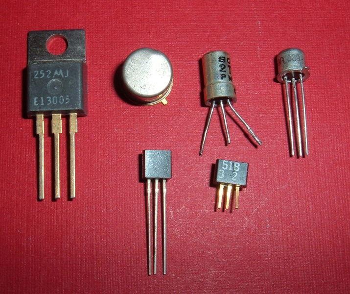
8 MODERN TRANSISTORS
.")
9 TERMINALS OF BJT Three terminals: Base (B) : very thin and lightly doped central region (little recombination). Emitter (E) and collector (C) are two outer regions sandwiching B.
10 TERMINALS AND OPERATONS
11 CIRCUIT SYMBOLS
12 CIRCUIT CONFIGURATION
13 OPERATION MODE CONTINUED Active: Most importance mode, e.g. for amplifier operation. The region where current curves are practically flat. Saturation: Barrier potential of the junctions cancel each other out causing a virtual short. Ideal transistor behaves like a closed switch

14 OPERATION MODE CONTINUED Cutoff: Current reduced to zero Ideal transistor behaves like an open switch.
15 TRANSISTOR PARAMETERS

16 OPERATION MODE
17 OUTPUT CHARACTERISTICS Region of Operation Active Description Small base current controls a large collector current Saturation V CE(sat) ~ 0.2V, V CE increases with I C I C Active Region I B Cutoff Achieved by reducing I B to 0, Ideally, I C will also equal 0. Saturation Region Cutoff Region I B = 0
18 LOAD LINE A line joining the intercept -VCC/RL on y-axis and VCC on x- axis is known as load line. A set of operating points Q1,Q2 etc is obtained at the intersection of load line and the output IC vs VCE characteristics. An operating point is called the quiescent point or Q point of a transistor when no signal is fed to the input circuit. To have the distortion free CE transistor output, Q point is always kept at the middle of the load line.
19 TRANSISTOR BIASING Need for transistor biasing : Need for transistor biasing is to fix the quiescent point at the middle of the load line and to fix it in the active region of output characteristics. The choice of location of Q-point depends upon the following factors : Value of available supply voltages Amplitude of input a.c signal Value of load resistance used Extent of distortion to be allowed in the output signal Despite of fixing of the Q-point in a transistor circuit it gets shifted with the use of circuit. Main reasons for the shifting of Q-point are as follows: Q-point is unstable as transistor parameters are temperature dependent Value of parameter rises with temperature and its value may vary from unit to unit Stability factor : It measures the change in collector current w.r.t. change in leakage current provided changes in and V BE are insignificant S = I C / I CO
20 METHODS OF TRANSISTOR BIASING Most commonly used methods for transistor biasing from one source of supply are the following : Biasing with feedback resistor or Fixed bias Collector to Base bias Biasing with emitter resistor Voltage divider biasing or Self bias
21 HYBRID PARAMETERS A transistor has three terminals, by keeping its one terminal common to input ans output circuit it becomes a two port network. Out of the four variables, V1,V2, i1 and i2 two are considered as independent variables and remaining two are dependent variables V 1 = f 1 (i 1,V 2 ) i 2 = f 2 (i 1,V 2 ) dv 1 = ( V 1 / i 1 ) di 1 + ( V 1 / V 2 ) dv 2 di 2 = ( i 2 / i 1 ) di 1 + ( i 2 / V 2 ) dv 2 h 11 = ( V 1 / i 1 ) h 12 = ( V 1 / V 2 ) Input impedance Reverse Voltage Gain h 21 = ( i 2 / i 1 ) h 22 = ( i 2 / V 2 ) dv 2 forward current ratio Output Admittance
Chapter 3 Bipolar Junction Transistors (BJT)
") Chapter 3 Bipolar Junction Transistors (BJT) Transistors In analog circuits, transistors are used in amplifiers and linear regulated power supplies. In digital circuits they function as electrical switches,
Chapter 3 Bipolar Junction Transistors (BJT) Transistors In analog circuits, transistors are used in amplifiers and linear regulated power supplies. In digital circuits they function as electrical switches,
Bipolar Junction Transistors
 Bipolar Junction Transistors Invented in 1948 at Bell Telephone laboratories Bipolar junction transistor (BJT) - one of the major three terminal devices Three terminal devices more useful than two terminal
An Introduction to Bipolar Junction Transistors. Prepared by Dr Yonas M Gebremichael, 2005
 An Introduction to Bipolar Junction Transistors Transistors Transistors are three port devices used in most integrated circuits such as amplifiers. Non amplifying components we have seen so far, such as
Electronic Circuits - Tutorial 07 BJT transistor 1
 Electronic Circuits - Tutorial 07 BJT transistor 1-1 / 20 - T & F # Question 1 A bipolar junction transistor has three terminals. T 2 For operation in the linear or active region, the base-emitter junction
COE/EE152: Basic Electronics. Lecture 5. Andrew Selasi Agbemenu. Outline
 COE/EE152: Basic Electronics Lecture 5 Andrew Selasi Agbemenu 1 Outline Physical Structure of BJT Two Diode Analogy Modes of Operation Forward Active Mode of BJTs BJT Configurations Early Effect Large
BJT. Bipolar Junction Transistor BJT BJT 11/6/2018. Dr. Satish Chandra, Assistant Professor, P P N College, Kanpur 1
 BJT Bipolar Junction Transistor Satish Chandra Assistant Professor Department of Physics P P N College, Kanpur www.satish0402.weebly.com The Bipolar Junction Transistor is a semiconductor device which
Transistor Characteristics
 Transistor Characteristics Topics covered in this presentation: Transistor Construction Transistor Operation Transistor Characteristics 1 of 15 The Transistor The transistor is a semiconductor device that
Figure1: Basic BJT construction.
 Chapter 4: Bipolar Junction Transistors (BJTs) Bipolar Junction Transistor (BJT) Structure The BJT is constructed with three doped semiconductor regions separated by two pn junctions, as in Figure 1(a).
Lecture 24: Bipolar Junction Transistors (1) Bipolar Junction Structure, Operating Regions, Biasing
 Bipolar Junction Structure, Operating Regions, Biasing") Lecture 24: Bipolar Junction Transistors (1) Bipolar Junction Structure, Operating Regions, Biasing BJT Structure the BJT is formed by doping three semiconductor regions (emitter, base, and collector)
Lecture 24: Bipolar Junction Transistors (1) Bipolar Junction Structure, Operating Regions, Biasing BJT Structure the BJT is formed by doping three semiconductor regions (emitter, base, and collector)
KOM2751 Analog Electronics :: Dr. Muharrem Mercimek :: YTU - Control and Automation Dept. 1 2 (CONT D - II) DIODE APPLICATIONS
 DIODE APPLICATIONS") KOM2751 Analog Electronics :: Dr. Muharrem Mercimek :: YTU - Control and Automation Dept. 1 2 (CONT D - II) DIODE APPLICATIONS Most of the content is from the textbook: Electronic devices and circuit theory,
KOM2751 Analog Electronics :: Dr. Muharrem Mercimek :: YTU - Control and Automation Dept. 1 2 (CONT D - II) DIODE APPLICATIONS Most of the content is from the textbook: Electronic devices and circuit theory,
Basic Electronics Prof. Dr. Chitralekha Mahanta Department of Electronics and Communication Engineering Indian Institute of Technology, Guwahati
 Basic Electronics Prof. Dr. Chitralekha Mahanta Department of Electronics and Communication Engineering Indian Institute of Technology, Guwahati Module: 2 Bipolar Junction Transistors Lecture-1 Transistor
PHY405F 2009 EXPERIMENT 6 SIMPLE TRANSISTOR CIRCUITS
 PHY405F 2009 EXPERIMENT 6 SIMPLE TRANSISTOR CIRCUITS Due Date (NOTE CHANGE): Thursday, Nov 12 th @ 5 pm; Late penalty in effect! Most active electronic devices are based on the transistor as the fundamental
Bipolar Junction Transistor (BJT)
") Bipolar Junction Transistor (BJT) - three terminal device - output port controlled by current flow into input port Structure - three layer sandwich of n-type and p-type material - npn and pnp transistors
Bipolar Junction Transistor (BJT) - three terminal device - output port controlled by current flow into input port Structure - three layer sandwich of n-type and p-type material - npn and pnp transistors
ET215 Devices I Unit 4A
 ITT Technical Institute ET215 Devices I Unit 4A Chapter 3, Section 3.1-3.2 This unit is divided into two parts; Unit 4A and Unit 4B Chapter 3 Section 3.1 Structure of Bipolar Junction Transistors The basic
Physics of Bipolar Transistor
 Physics of Bipolar Transistor Motivations - In many electronic applications, amplifier is the most fundamental building block. Ex Audio amplifier: amplifies electric signal to drive a speaker RF Power
Analog Electronics. Electronic Devices, 9th edition Thomas L. Floyd Pearson Education. Upper Saddle River, NJ, All rights reserved.
 Analog Electronics BJT Structure The BJT has three regions called the emitter, base, and collector. Between the regions are junctions as indicated. The base is a thin lightly doped region compared to the
Lecture 3: Transistors
 Lecture 3: Transistors Now that we know about diodes, let s put two of them together, as follows: collector base emitter n p n moderately doped lightly doped, and very thin heavily doped At first glance,
EXPERIMENT 12: SIMULATION STUDY OF DIFFERENT BIASING CIRCUITS USING NPN BJT
 EXPERIMENT 12: SIMULATION STUDY OF DIFFERENT BIASING CIRCUITS USING NPN BJT AIM: 1) To study different BJT DC biasing circuits 2) To design voltage divider bias circuit using NPN BJT SOFTWARE TOOL: PC
Student Lecture by: Giangiacomo Groppi Joel Cassell Pierre Berthelot September 28 th 2004
 Student Lecture by: Giangiacomo Groppi Joel Cassell Pierre Berthelot September 28 th 2004 Lecture outline Historical introduction Semiconductor devices overview Bipolar Junction Transistor (BJT) Field
Lecture 12. Bipolar Junction Transistor (BJT) BJT 1-1
 BJT 1-1") Lecture 12 Bipolar Junction Transistor (BJT) BJT 1-1 Course Info Lecture hours: 4 Two Lectures weekly (Saturdays and Wednesdays) Location: K2 Time: 1:40 pm Tutorial hours: 2 One tutorial class every week
Lecture 12 Bipolar Junction Transistor (BJT) BJT 1-1 Course Info Lecture hours: 4 Two Lectures weekly (Saturdays and Wednesdays) Location: K2 Time: 1:40 pm Tutorial hours: 2 One tutorial class every week
Transistors and Applications
 Chapter 17 Transistors and Applications DC Operation of Bipolar Junction Transistors (BJTs) The bipolar junction transistor (BJT) is constructed with three doped semiconductor regions separated by two
CHAPTER 3: BIPOLAR JUNCION TRANSISTOR DR. PHẠM NGUYỄN THANH LOAN
 CHAPTER 3: BIPOLAR JUNCION TRANSISTOR DR. PHẠM NGUYỄN THANH LOAN Hanoi, 9/24/2012 Contents 2 Structure and operation of BJT Different configurations of BJT Characteristic curves DC biasing method and analysis
Electronics EECE2412 Spring 2017 Exam #2
 Electronics EECE2412 Spring 2017 Exam #2 Prof. Charles A. DiMarzio Department of Electrical and Computer Engineering Northeastern University 30 March 2017 File:12198/exams/exam2 Name: : General Rules:
5.1 BJT Device Structure and Physical Operation
 11/28/2004 section 5_1 BJT Device Structure and Physical Operation blank 1/2 5.1 BJT Device Structure and Physical Operation Reading Assignment: pp. 377-392 Another kind of transistor is the Bipolar Junction
Bipolar junction transistors.
 Bipolar junction transistors. Third Semester Course code : 15EECC202 Analog electronic circuits (AEC) Team: Dr. Nalini C Iyer, R.V. Hangal, Sujata N, Prashant A, Sneha Meti AEC Team, Faculty, School of
FIELD EFFECT TRANSISTORS MADE BY : GROUP (13)/PM
/PM") FIELD EFFECT TRANSISTORS MADE BY : GROUP (13)/PM THE FIELD EFFECT TRANSISTOR (FET) In 1945, Shockley had an idea for making a solid state device out of semiconductors. He reasoned that a strong electrical
FIELD EFFECT TRANSISTORS MADE BY : GROUP (13)/PM THE FIELD EFFECT TRANSISTOR (FET) In 1945, Shockley had an idea for making a solid state device out of semiconductors. He reasoned that a strong electrical
ECE 310 Microelectronics Circuits
 ECE 310 Microelectronics Circuits Bipolar Transistors Dr. Vishal Saxena (vishalsaxena@boisetstate.edu) Jan 20, 2014 Vishal Saxena 1 Bipolar Transistor n the chapter, we will study the physics of bipolar
Tutorial 2 BJTs, Transistor Bias Circuits, BJT Amplifiers FETs and FETs Amplifiers. Part 1: BJTs, Transistor Bias Circuits and BJT Amplifiers
 Tutorial 2 BJTs, Transistor Bias Circuits, BJT Amplifiers FETs and FETs Amplifiers Part 1: BJTs, Transistor Bias Circuits and BJT Amplifiers 1. Explain the purpose of a thin, lightly doped base region.
UNIT I - TRANSISTOR BIAS STABILITY
 UNIT I - TRANSISTOR BIAS STABILITY OBJECTIVE On the completion of this unit the student will understand NEED OF BIASING CONCEPTS OF LOAD LINE Q-POINT AND ITS STABILIZATION AND COMPENSATION DIFFERENT TYPES
Chapter 3-2 Semiconductor devices Transistors and Amplifiers-BJT Department of Mechanical Engineering
 MEMS1082 Chapter 3-2 Semiconductor devices Transistors and Amplifiers-BJT Bipolar Transistor Construction npn BJT Transistor Structure npn BJT I = I + E C I B V V BE CE = V = V B C V V E E Base-to-emitter
Chapter Two "Bipolar Transistor Circuits"
 Chapter Two "Bipolar Transistor Circuits" 1.TRANSISTOR CONSTRUCTION:- The transistor is a three-layer semiconductor device consisting of either two n- and one p-type layers of material or two p- and one
Chapter 5 Transistor Bias Circuits
 Chapter 5 Transistor Bias Circuits Objectives Discuss the concept of dc biasing of a transistor for linear operation Analyze voltage-divider bias, base bias, and collector-feedback bias circuits. Basic
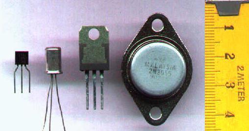
The first transistor. (Courtesy Bell Telephone Laboratories.)
") Fig. 3.1 The first transistor. (Courtesy Bell Telephone Laboratories.) Fig. 3.2 Types of transistors: (a) pnp; (b) npn. : (a) pnp; : (b) npn Fig. 3.3 Forward-biased junction of a pnp transistor. Fig. 3.4
Fig. 3.1 The first transistor. (Courtesy Bell Telephone Laboratories.) Fig. 3.2 Types of transistors: (a) pnp; (b) npn. : (a) pnp; : (b) npn Fig. 3.3 Forward-biased junction of a pnp transistor. Fig. 3.4
10 Semiconductors - Transistors
 10 Semiconductors - Transistors The transistor was invented in the late 1940s. Credit for its invention is given to three Bell Laboratories scientists, John Bardeen, Walter Brattain, and William Shockley.
(a) BJT-OPERATING MODES & CONFIGURATIONS
 BJT-OPERATING MODES & CONFIGURATIONS") (a) BJT-OPERATING MODES & CONFIGURATIONS 1. The leakage current I CBO flows in (a) The emitter, base and collector leads (b) The emitter and base leads. (c) The emitter and collector leads. (d) The base
(a) BJT-OPERATING MODES & CONFIGURATIONS 1. The leakage current I CBO flows in (a) The emitter, base and collector leads (b) The emitter and base leads. (c) The emitter and collector leads. (d) The base
Analog & Digital Electronics Course No: PH-218
 Analog & Digital Electronics Course No: PH-218 Lec-5: Bipolar Junction Transistor (BJT) Course nstructors: Dr. A. P. VAJPEY Department of Physics, ndian nstitute of Technology Guwahati, ndia 1 Bipolar
Electronic Circuits EE359A
 Electronic Circuits EE359A Bruce McNair B206 bmcnair@stevens.edu 201-216-5549 Lecture 4 0 Bipolar Junction Transistors (BJT) Small Signal Analysis Graphical Analysis / Biasing Amplifier, Switch and Logic
ITT Technical Institute. ET215 Devices 1. Unit 6 Chapter 3, Sections
 ITT Technical Institute ET215 Devices 1 Unit 6 Chapter 3, Sections 3.7-3.9 Chapter 3 Section 3.7 The Bipolar Transistor as a Switch Objectives: Explain how a transistor can be used as a switch 1. Compute
EE105 Fall 2014 Microelectronic Devices and Circuits. NPN Bipolar Junction Transistor (BJT)
") EE105 Fall 2014 Microelectronic Devices and Circuits Prof. Ming C. Wu wu@eecs.berkeley.edu 511 utardja Dai Hall (DH) 1 NPN Bipolar Junction Transistor (BJT) Forward Bias Reverse Bias Hole Flow Electron
EE105 Fall 2014 Microelectronic Devices and Circuits Prof. Ming C. Wu wu@eecs.berkeley.edu 511 utardja Dai Hall (DH) 1 NPN Bipolar Junction Transistor (BJT) Forward Bias Reverse Bias Hole Flow Electron
TRANSISTOR TRANSISTOR
 It is made up of semiconductor material such as Si and Ge. Usually, it comprises of three terminals namely, base, emitter and collector for providing connection to the external circuit. Today, some transistors
ME 4447 / 6405 Student Lecture. Transistors. Abiodun Otolorin Michael Abraham Waqas Majeed
 ME 4447 / 6405 Student Lecture Transistors Abiodun Otolorin Michael Abraham Waqas Majeed Lecture Overview Transistor? History Underlying Science Properties Types of transistors Bipolar Junction Transistors
Bipolar Junction Transistors (BJTs)
") C H A P T E R 6 Bipolar Junction Transistors (BJTs) Figure 6.1 A simplified structure of the npn transistor and pnp transistor. Table 6.1: BJT modes of Operation Mode Cutoff Active Saturation EBJ Reverse
C H A P T E R 6 Bipolar Junction Transistors (BJTs) Figure 6.1 A simplified structure of the npn transistor and pnp transistor. Table 6.1: BJT modes of Operation Mode Cutoff Active Saturation EBJ Reverse
FET, BJT, OpAmp Guide
 FET, BJT, OpAmp Guide Alexandr Newberry UCSD PHYS 120 June 2018 1 FETs 1.1 What is a Field Effect Transistor? Figure 1: FET with all relevant values labelled. FET stands for Field Effect Transistor, it
Transistor fundamentals Nafees Ahamad
 Transistor fundamentals Nafees Ahamad Asstt. Prof., EECE Deptt, DIT University, Dehradun Website: www.eedofdit.weebly.com Transistor A transistor consists of two PN junctions formed by sandwiching either
Emitter base bias. Collector base bias Active Forward Reverse Saturation forward Forward Cut off Reverse Reverse Inverse Reverse Forward
 SEMICONDUCTOR PHYSICS-2 [Transistor, constructional characteristics, biasing of transistors, transistor configuration, transistor as an amplifier, transistor as a switch, transistor as an oscillator] Transistor
Review Energy Bands Carrier Density & Mobility Carrier Transport Generation and Recombination
 Review Energy Bands Carrier Density & Mobility Carrier Transport Generation and Recombination Current Transport: Diffusion, Thermionic Emission & Tunneling For Diffusion current, the depletion layer is
THE JFET. Script. Discuss the JFET and how it differs from the BJT. Describe the basic structure of n-channel and p -channel JFETs
 Course: B.Sc. Applied Physical Science (Computer Science) Year & Sem.: Ist Year, Sem - IInd Subject: Electronics Paper No.: V Paper Title: Analog Circuits Lecture No.: 12 Lecture Title: Analog Circuits
Structure of Actual Transistors
 4.1.3. Structure of Actual Transistors Figure 4.7 shows a more realistic BJT cross-section Collector virtually surrounds entire emitter region This makes it difficult for electrons injected into base to
7. Bipolar Junction Transistor
 41 7. Bipolar Junction Transistor 7.1. Objectives - To experimentally examine the principles of operation of bipolar junction transistor (BJT); - To measure basic characteristics of n-p-n silicon transistor
Bipolar Junction Transistors (BJTs) Overview
 Overview") 1 Bipolar Junction Transistors (BJTs) Asst. Prof. MONTREE SIRIPRUCHYANUN, D. Eng. Dept. of Teacher Training in Electrical Engineering, Faculty of Technical Education King Mongkut s Institute of Technology
1 Bipolar Junction Transistors (BJTs) Asst. Prof. MONTREE SIRIPRUCHYANUN, D. Eng. Dept. of Teacher Training in Electrical Engineering, Faculty of Technical Education King Mongkut s Institute of Technology
ECE 440 Lecture 29 : Introduction to the BJT-I Class Outline:
 ECE 440 Lecture 29 : Introduction to the BJT-I Class Outline: Narrow-Base Diode BJT Fundamentals BJT Amplification Things you should know when you leave Key Questions How does the narrow-base diode multiply
ELECTRONICS LAB. PART 3
 ELECTRONICS LAB. PART 3 Yrd. Doç. Dr. Taha İMECİ Arş. Gör. Ezgi YAMAÇ Arş. Gör. Ufuk ŞANVER İSTANBUL COMMERCE UNIVERSITY Contents TRANSISTORS... 2 5.1 INTRODUCTION... 2 5.2 OPERATION OF TRANSISTORS...
The shape of the waveform will be the same, but its level is shifted either upward or downward. The values of the resistor R and capacitor C affect
 Diode as Clamper A clamping circuit is used to place either the positive or negative peak of a signal at a desired level. The dc component is simply added or subtracted to/from the input signal. The clamper
Electronic Troubleshooting
 Electronic Troubleshooting Chapter 3 Bipolar Transistors Most devices still require some individual (discrete) transistors Used to customize operations Interface to external devices Understanding their
Shankersinh Vaghela Bapu Institute of Technology INDEX
 Shankersinh Vaghela Bapu Institute of Technology Diploma EE Semester III 3330905: ELECTRONIC COMPONENTS AND CIRCUITS INDEX Sr. No. Title Page Date Sign Grade 1 Obtain I-V characteristic of Diode. 2 To
ECE 334: Electronic Circuits Lecture 2: BJT Large Signal Model
 Faculty of Engineering ECE 334: Electronic Circuits Lecture 2: BJT Large Signal Model Agenda I & V Notations BJT Devices & Symbols BJT Large Signal Model 2 I, V Notations (1) It is critical to understand
Electronics I Circuit Drawings. Robert R. Krchnavek Rowan University Spring, 2018
 Electronics I Circuit Drawings Robert R. Krchnavek Rowan University Spring, 2018 Ideal Diode Piecewise Linear Models of a Diode Piecewise Linear Models of a Diode 1 r d Piecewise Linear Models of a Diode
BJT Amplifier. Superposition principle (linear amplifier)
") BJT Amplifier Two types analysis DC analysis Applied DC voltage source AC analysis Time varying signal source Superposition principle (linear amplifier) The response of a linear amplifier circuit excited
BJT Amplifier Two types analysis DC analysis Applied DC voltage source AC analysis Time varying signal source Superposition principle (linear amplifier) The response of a linear amplifier circuit excited
Chapter 8. Field Effect Transistor
 Chapter 8. Field Effect Transistor Field Effect Transistor: The field effect transistor is a semiconductor device, which depends for its operation on the control of current by an electric field. There
The Common Source JFET Amplifier
 The Common Source JFET Amplifier Small signal amplifiers can also be made using Field Effect Transistors or FET's for short. These devices have the advantage over bipolar transistors of having an extremely
FIELD EFFECT TRANSISTOR (FET) 1. JUNCTION FIELD EFFECT TRANSISTOR (JFET)
 1. JUNCTION FIELD EFFECT TRANSISTOR (JFET)") FIELD EFFECT TRANSISTOR (FET) The field-effect transistor (FET) is a three-terminal device used for a variety of applications that match, to a large extent, those of the BJT transistor. Although there
FIELD EFFECT TRANSISTOR (FET) The field-effect transistor (FET) is a three-terminal device used for a variety of applications that match, to a large extent, those of the BJT transistor. Although there
EE301 Electronics I , Fall
 EE301 Electronics I 2018-2019, Fall 1. Introduction to Microelectronics (1 Week/3 Hrs.) Introduction, Historical Background, Basic Consepts 2. Rewiev of Semiconductors (1 Week/3 Hrs.) Semiconductor materials
EXPERIMENT 5 CURRENT AND VOLTAGE CHARACTERISTICS OF BJT
 EXPERIMENT 5 CURRENT AND VOLTAGE CHARACTERISTICS OF BJT 1. OBJECTIVES 1.1 To practice how to test NPN and PNP transistors using multimeter. 1.2 To demonstrate the relationship between collector current
C H A P T E R 6 Bipolar Junction Transistors (BJTs)
") C H A P T E R 6 Bipolar Junction Transistors (BJTs) Figure 6.1 A simplified structure of the npn transistor and pnp transistor. Table 6.1: BJT modes of Operation Mode EBJ CBJ Cutoff Reverse Reverse Active
C H A P T E R 6 Bipolar Junction Transistors (BJTs) Figure 6.1 A simplified structure of the npn transistor and pnp transistor. Table 6.1: BJT modes of Operation Mode EBJ CBJ Cutoff Reverse Reverse Active
Chapter 3. Bipolar Junction Transistors
 Chapter 3. Bipolar Junction Transistors Outline: Fundamental of Transistor Common-Base Configuration Common-Emitter Configuration Common-Collector Configuration Introduction The transistor is a three-layer
EEE118: Electronic Devices and Circuits
 EEE118: Electronic Devices and Circuits Lecture XI James E Green Department of Electronic Engineering University of Sheffield j.e.green@sheffield.ac.uk Review Review Introduced the idea of a dynamic resistance
Lecture (09) Bipolar Junction Transistor 3
 Bipolar Junction Transistor 3") Lecture (09) Bipolar Junction Transistor 3 By: Dr. Ahmed ElShafee ١ I THE BJT AS AN AMPLIFIER Amplification is the process of linearly increasing the amplitude of an electrical signal and is one of the
Lecture (09) Bipolar Junction Transistor 3 By: Dr. Ahmed ElShafee ١ I THE BJT AS AN AMPLIFIER Amplification is the process of linearly increasing the amplitude of an electrical signal and is one of the
Current Mirrors. Basic BJT Current Mirror. Current mirrors are basic building blocks of analog design. Figure shows the basic NPN current mirror.
 Current Mirrors Basic BJT Current Mirror Current mirrors are basic building blocks of analog design. Figure shows the basic NPN current mirror. For its analysis, we assume identical transistors and neglect
Field Effect Transistors (npn)
") Field Effect Transistors (npn) gate drain source FET 3 terminal device channel e - current from source to drain controlled by the electric field generated by the gate base collector emitter BJT 3 terminal
Field Effect Transistors (npn) gate drain source FET 3 terminal device channel e - current from source to drain controlled by the electric field generated by the gate base collector emitter BJT 3 terminal
UNIT 3 Transistors JFET
 UNIT 3 Transistors JFET Mosfet Definition of BJT A bipolar junction transistor is a three terminal semiconductor device consisting of two p-n junctions which is able to amplify or magnify a signal. It
Transistors CHAPTER 3.1 INTRODUCTION
 CHAPTER 3 Bipolar Junction Transistors 3. INTRODUCTION During the period 904 947, the vacuum tube was undoubtedly the electronic device of interest and development. In 904, the vacuum-tube diode was introduced
Module 2. B.Sc. I Electronics. Developed by: Mrs. Neha S. Joshi Asst. Professor Department of Electronics Willingdon College, Sangli
 Module 2 B.Sc. I Electronics Developed by: Mrs. Neha S. Joshi Asst. Professor Department of Electronics Willingdon College, Sangli BIPOLAR JUNCTION TRANSISTOR SCOPE OF THE CHAPTER- This chapter introduces
SEMICONDUCTOR ELECTRONICS: MATERIALS, DEVICES AND SIMPLE CIRCUITS. Class XII : PHYSICS WORKSHEET
 SEMICONDUCT ELECTRONICS: MATERIALS, DEVICES AND SIMPLE CIRCUITS Class XII : PHYSICS WKSHEET 1. How is a n-p-n transistor represented symbolically? (1) 2. How does conductivity of a semiconductor change
EIE209 Basic Electronics. Transistor Devices. Contents BJT and FET Characteristics Operations. Prof. C.K. Tse: T ransistor devices
 EIE209 Basic Electronics Transistor Devices Contents BJT and FET Characteristics Operations 1 What is a transistor? Three-terminal device whose voltage-current relationship is controlled by a third voltage
Chapter 4 DC Biasing BJTs. BJTs
 hapter 4 D Biasing BJTs BJTs Biasing Biasing: The D voltages applied to a transistor in order to turn it on so that it can amplify the A signal. Operating Point The D input establishes an operating or
Mechatronics and Measurement. Lecturer:Dung-An Wang Lecture 2
 Mechatronics and Measurement Lecturer:Dung-An Wang Lecture 2 Lecture outline Reading:Ch3 of text Today s lecture Semiconductor 2 Diode 3 4 Zener diode Voltage-regulator diodes. This family of diodes exhibits
When you have completed this exercise, you will be able to determine the ac operating characteristics of
 When you have completed this exercise, you will be able to determine the ac operating characteristics of multimeter and an oscilloscope. A sine wave generator connected between the transistor and ground
DEPARTMENT OF ELECTRONICS AND COMMUNICATION ENGINEERING III SEMESTER EC 6304 ELECTRONIC CIRCUITS I. (Regulations 2013)
") DEPARTMENT OF ELECTRONICS AND COMMUNICATION ENGINEERING III SEMESTER EC 6304 ELECTRONIC CIRCUITS I (Regulations 2013 UNIT-1 Part A 1. What is a Q-point? [N/D 16] The operating point also known as quiescent
DEPARTMENT OF ELECTRONICS AND COMMUNICATION ENGINEERING III SEMESTER EC 6304 ELECTRONIC CIRCUITS I (Regulations 2013 UNIT-1 Part A 1. What is a Q-point? [N/D 16] The operating point also known as quiescent
Chapter 2. Bipolar Junction Transistor
 Chapter 2 ipolar Junction Transistor 2.0 History The name bipolar is used because both types of carriers namely hole and electron are used in the transistor, as opposed to field effect transistor, which
Lecture 9 Transistors
 Lecture 9 Transistors Physics Transistor/transistor logic CMOS logic CA 1947 http://www.extremetech.com/extreme/164301-graphenetransistors-based-on-negative-resistance-could-spell-theend-of-silicon-and-semiconductors
SUMMER 13 EXAMINATION Subject Code: Model Answer Page No: / N
 Important Instructions to examiners: 1) The answers should be examined by key words and not as word-to-word as given in the model answer scheme. 2) The model answer and the answer written by candidate
I C I E =I B = I C 1 V BE 0.7 V
 Guide to NPN Amplifier Analysis Jason Woytowich 1. Transistor characteristics A BJT has three operating modes cutoff, active, and saturation. For applications, like amplifiers, where linear characteristics
SRM INSTITUTE OF SCIENCE AND TECHNOLOGY (DEEMED UNIVERSITY)
") SRM INSTITUTE OF SCIENCE AND TECHNOLOGY (DEEMED UNIVERSITY) QUESTION BANK I YEAR B.Tech (II Semester) ELECTRONIC DEVICES (COMMON FOR EC102, EE104, IC108, BM106) UNIT-I PART-A 1. What are intrinsic and
SRM INSTITUTE OF SCIENCE AND TECHNOLOGY (DEEMED UNIVERSITY) QUESTION BANK I YEAR B.Tech (II Semester) ELECTRONIC DEVICES (COMMON FOR EC102, EE104, IC108, BM106) UNIT-I PART-A 1. What are intrinsic and
Concepts to be Covered
 Introductory Medical Device Prototyping Analog Circuits Part 2 Semiconductors, http://saliterman.umn.edu/ Department of Biomedical Engineering, University of Minnesota Concepts to be Covered Semiconductors
Physics 364, Fall 2012, reading due your answers to by 11pm on Thursday
 Physics 364, Fall 2012, reading due 2012-10-25. Email your answers to ashmansk@hep.upenn.edu by 11pm on Thursday Course materials and schedule are at http://positron.hep.upenn.edu/p364 Assignment: (a)
Bipolar Junction Transistor (BJT)
") Bipolar Junction Transistor (BJT) 1 Objectives To understand the structure of BJT. To explain and analyze the basic transistor circuits. To use transistors as an amplifier and electronic switch. To design
Bipolar Junction Transistor (BJT) 1 Objectives To understand the structure of BJT. To explain and analyze the basic transistor circuits. To use transistors as an amplifier and electronic switch. To design
UNIT 4 BIASING AND STABILIZATION
 UNIT 4 BIASING AND STABILIZATION TRANSISTOR BIASING: To operate the transistor in the desired region, we have to apply external dec voltages of correct polarity and magnitude to the two junctions of the
PHYS 3050 Electronics I
 PHYS 3050 Electronics I Chapter 4. Semiconductor Diodes and Transistors Earth, Moon, Mars, and Beyond Dr. Jinjun Shan, Associate Professor of Space Engineering Department of Earth and Space Science and
I E I C since I B is very small
 Figure 2: Symbols and nomenclature of a (a) npn and (b) pnp transistor. The BJT consists of three regions, emitter, base, and collector. The emitter and collector are usually of one type of doping, while
Field - Effect Transistor
 Page 1 of 6 Field - Effect Transistor Aim :- To draw and study the out put and transfer characteristics of the given FET and to determine its parameters. Apparatus :- FET, two variable power supplies,
Communication Microelectronics (W17)
") Communication Microelectronics (W17) Lecture 4: Bipolar Junction Transistor Assistant Professor Office: C3.315 E-mail: eman.azab@guc.edu.eg 1 Bipolar Junction Transistor (BJT) Physical Structure and I-V
Communication Microelectronics (W17) Lecture 4: Bipolar Junction Transistor Assistant Professor Office: C3.315 E-mail: eman.azab@guc.edu.eg 1 Bipolar Junction Transistor (BJT) Physical Structure and I-V
DISCUSSION The best way to test a transistor is to connect it in a circuit that uses the transistor.
 Exercise 1: EXERCISE OBJECTIVE When you have completed this exercise, you will be able to test a transistor by forward biasing and reverse biasing the junctions. You will verify your results with an ohmmeter.
EXPERIMENT #3 TRANSISTOR BIASING
 EXPERIMENT #3 TRANSISTOR BIASING Bias (operating point) for a transistor is established by specifying the quiescent (D.C., no signal) values of collector-emitter voltage V CEQ and collector current I CQ.
55:041 Electronic Circuits
 55:041 Electronic Circuits Output Stages and Power Amplifiers Sections of Chapter 8 A. Kruger Power + Output Stages1 Power Amplifiers, Power FETS & BJTs Audio (stereo) MP3 Players Motor controllers Servo
EDC UNIT IV- Transistor and FET Characteristics EDC Lesson 9- ", Raj Kamal, 1
 EDC UNIT IV- Transistor and FET Characteristics Lesson-9: JFET and Construction of JFET 2008 EDC Lesson 9- ", Raj Kamal, 1 1. Transistor 2008 EDC Lesson 9- ", Raj Kamal, 2 Transistor Definition The transferred-resistance
Transistor Biasing. DC Biasing of BJT. Transistor Biasing. Transistor Biasing 11/23/2018
 Transistor Biasing DC Biasing of BJT Satish Chandra Assistant Professor Department of Physics P P N College, Kanpur www.satish0402.weebly.com A transistors steady state of operation depends a great deal
Laboratory #5 BJT Basics and MOSFET Basics
 Laboratory #5 BJT Basics and MOSFET Basics I. Objectives 1. Understand the physical structure of BJTs and MOSFETs. 2. Learn to measure I-V characteristics of BJTs and MOSFETs. II. Components and Instruments
Transistor Biasing Nafees Ahamad
 Transistor Biasing Nafees Ahamad Asstt. Prof., EECE Deptt, DIT University, Dehradun Website: www.eedofdit.weebly.com Introduction The basic function of transistor is to do amplification. (CE connection)
CO2005: Electronics I. Transistor (BJT) Electronics I, Neamen 3th Ed. 1
 Electronics I, Neamen 3th Ed. 1") O2005: Electronics The Bipolar Junction Transistor (BJT) Electronics, Neamen 3th Ed. 1 Bipolar Transistor Structures N P 17 10 N D 19 10 N D 15 10 Electronics, Neamen 3th Ed. 2 Forward-Active Mode in the
O2005: Electronics The Bipolar Junction Transistor (BJT) Electronics, Neamen 3th Ed. 1 Bipolar Transistor Structures N P 17 10 N D 19 10 N D 15 10 Electronics, Neamen 3th Ed. 2 Forward-Active Mode in the
Sonoma State University Department of Engineering Science Fall 2017
 ES-110 Laboratory Introduction to Engineering & Laboratory Experience Saeid Rahimi, Ph.D. Lab 7 Introduction to Transistors Introduction As we mentioned before, diodes have many applications which are