Passive Device Characterization for 60-GHz CMOS Power Amplifiers
|
|
|
- Jason Norris
- 5 years ago
- Views:
Transcription

1 Passive Device Characterization for 60-GHz CMOS Power Amplifiers Kenichi Okada, Kota Matsushita, Naoki Takayama, Shogo Ito, Ning Li, and Akira Tokyo Institute of Technology, Japan 2009/4/20
2 Motivation 1 60GHz unlicensed band Australia America, Canada Europe Australia America, Canada Japan Europe Japan Frequency [GHz] Frequency [GHz] [1] 9GHz-BW around 60GHz Several-Gbps wireless communication Use of CMOS process Fab. cost is very important to generalize it. RF&BB mixed chip can be realized.

3 Our target 2 8b DAC 8b DAC DAC LNA LPF LPF Buff Buff VGA VGA ADC ADC DAC 60GHz Tripler with I/Q ch 20GHz PLL PLL 36MHz TCXO ch 3456MHz PLL PLL DAC Digital Base Band PA DAC 8b+6b DAC 8b+3b LPF LPF DAC DAC DAC 8b DAC 8b Reg. bank addr/data 60GHz 2.16GHz-full 4ch direct-conversion by CMOS Tr QPSK 3Gbps & 16QAM 6Gbps & 64QAM 9Gbps IEEE c conformance Dynamic power management: <300mW for RF front-end

4 Circuit blocks of 60GHz transceiver 3 60GHz LNA Down-Mixer 20GHz PLL 60GHz PA Up-Mixer 60GHz Tripler with quadrature output
 The wave length is very short, (2) Tr s gain is very small, and (3) Loss of TL is")

5 mmw CMOS circuit design 4 Matching is very important for mmw circuit design, because (1) The wave length is very short, (2) Tr s gain is very small, and (3) Loss of TL is very large. Matching blocks Inductor@ Transmission line@60 At 60GHz, every interconnects should be dealt with as a distributed component. The accurate characterization is required.
 Transmission line (various length & Z0) Branch &")

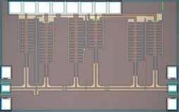
6 Overview of device characterization 5 Initial T.O. Second T.O. Initial T.O. for Modeling Transistors (CS, CG with various layouts) Transmission line (various length & Z0) Branch & bend line Spiral inductor Balun Series capacitor Decoupling capacitor De-embedding patterns 1-stage amplifier for the model evaluation DC probe Second T.O. Circuit building blocks Whole system
7 Overview of characterization 6 Transmission line Branch & bend line Decoupling capacitor De-embedding patterns 1-stage amplifier DC probe 4-stage power amplifier


8 Dummy metal 7 To avoid random production of dummy metal, it is manually placed to keep good reproducibility. Metal dummy 40um Metal dummy


9 Tile-base layout 8 Each component is previously measured and modeled. The same layout is utilized to maintain modeling accuracy. 5µm pitch T-Junction Tr TL C L-Bend MIM TL RF PAD GND-Tile
 (2S ) 1 21 2 2 (2S 11 ) 2 1")

10 Transmission line in CMOS chip 9 Guided microstrip line GND Signal GND e γl K S11 + S 21 = ± K 2S21 ( S = S ) (2S ) (2S 11 ) Z 2 = Z 2 0 (1 + S (1 S γ = α + j β Slow-wave coplanar-waveguide is also utilized depending on a required characteristic impedance. ) ) 2 2 S S
11 Cross-sectional structure Ω/mm G S G Top metal 1.2um 8.0um 15um 10um 15um 40um Metal 1(shield/slit) Substrate 320um 0.2um 0.3um
12 Modeling of transmission line 11 ADS s CPW model To meet measured α, β, Q and Z 0, substrate model is individually extracted for each structure.
13 Transmission line (200µm) Measurement Model Measurement Model Q 20 Z 0 [Ω] Frequency [GHz] Frequency [GHz] Improved Mangan s method is utilized with 200µm and 400µm transmission lines. [2] A.M. Mangan, et al., IEEE Trans. on Electron Devices, vol. 53, no. 2, pp , Feb. 2006
14 Transmission line (400µm) Measurement Model Measurement Model Q 20 Z 0 [Ω] Frequency [GHz] Frequency [GHz] 400µm of transmission line has almost the same characteristics with that of 200µm, which is a good proof of accurate modeling.
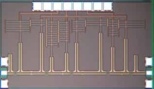
15 Overview of characterization 14 Transmission line Branch & bend line Decoupling capacitor De-embedding patterns 1-stage amplifier DC probe 4-stage power amplifier


16 Branch & bend modeling 15 with 4 bending parts with 200µm shunt TL with 300µm shunt TL Each red-box part is characterized as a combination of optimized transmission lines.


17 T-junction modeling 16 Straightforward modeling Lower Z0 TLs are utilized, and Z0 is adjusted for the measurement results. Dummy metal causes unexpected response.
18 Experimental results for T-junction 17 0 No model ADS model S(2,1) [db] Our model Measurement Without T model With T model Modeling Frequency [GHz] T-junction with 200µm shunt TL S(2,1) [db] Our model extracted from 200µm TEG Measurement Modeling Frequency [GHz] T-junction with 300µm shunt TL
19 Overview of characterization 18 Transmission line Branch & bend line Decoupling capacitor De-embedding patterns 1-stage amplifier DC probe 4-stage power amplifier

20 MIM capacitor for de-coupling 19 Area efficiency is large, but the self-resonance freq. is low. The regular layout of MIM cap. cannot be used at 60GHz.


21 Interdigital MIM capacitor 20 Interdigital structure with the optimized finger length is utilized. to DC-Pad MIM cap. is modeled as a lowimpedance transmission line. to Matching block


22 Distributed modeling of MIM cap. Modeled as a transmission line 21 reflection 1-67GHz
23 Overview of characterization 22 Transmission line Branch & bend line Decoupling capacitor De-embedding patterns 1-stage amplifier DC probe 4-stage power amplifier
 Comparison between model and")
24 An evaluation using a 1-stage amplifier 23 Transmission line De-coupling cap. :CS Transistor (De-embedded S-parameter) Comparison between model and measurement.
25 Model evaluation in input&output reflection 24 S11(gate-side reflection) S22(drain-side reflection) 60GHz Measurement with de-coupling model without de-coupling model De-coupling MIM model is required for reliable design. 90nm CMOS is used.
26 Other modeling issues 25 De-embedding Transistor layout optimization Spiral inductor Balun RF Pad DC probe / bonding wire / bump / filler / PCB

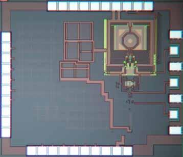
27 In-house PDK 26 PVT C MIM TL TL with L/T NMOS PMOS R RF PAD DC probe Varactor MIM MOS cap Each component is implemented as an in-house PDK for Agilent ADS.
28 Overview of characterization 27 Transmission line Branch & bend line Decoupling capacitor De-embedding patterns 1-stage amplifier DC probe 4-stage power amplifier
29 4-stage class-a Power Amplifier CMOS 65nm process Short stub 28 Vds4 370 m Vds3 5.75pF 290 m Vgs4 5.75pF 310 m 7.25pF 75fF RFout 70 m 140 m 20 m 100fF 50 m W=80 m 150 m W=80 m
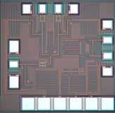
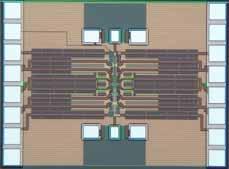
30 Chip micrograph 60GHz CMOS PA mm IN OUT surface ground plane 1.5mm CMOS 65nm process
31 Measurement results S21: 16.4dB S11: <-8dB S22: <-10dB
32 Measurement results 31 Power gain: 16.4dB P1dB: 4.6dBm PDC: 122mW
33 Measurement summary 32 Reference Technology Freq. [GHz] Gain [db] P1dB [dbm] 1dB [%] PDC [mw] VDD [V] [4] JSSCC nm CMOS [5] RFIC nm CMOS [6] ISSCC nm CMOS [7] ISSCC nm CMOS [8] ISSCC nm CMOS [9] ISSCC nm CMOS [10] ISSCC nm CMOS [11] MWCL nm CMOS This work 65nm CMOS [4] T.Yao, et al., JSSC 2007(Tronto Univ.) [5] T.L.Rocca, et al., RFIC 2008 (UCLA) [6] T.Suzuki, et al., ISSCC 2008 (Fujitsu) [7] D. Chowdhury, et al., ISSCC 2008 (UCB) [8] M. Tanomura, et al., ISSCC 2008 (NEC) [9] W.L. Chan, et al., ISSCC 2009 (Delft Univ.) [10] K. Raczkowski, et al., ISSCC 2009 (KU Leuven&IMEC) [11] J.-L.Kuo, et al., MWCL 2009 (NTU)
34 Summary & Conclusion 33 In this presentation, I presented a modeling approach to design a 60GHz CMOS amplifiers. 1. Design issue of TL on CMOS chips is different from that of compound semiconductors. e.g., dummy metal, lossy substrate, large conductive loss, etc 2. Branch modeling 3. Distributed modeling of de-couple MIM cap. 4. Evaluation using a 1-stage amplifier By the proposed modeling method, 60GHz power amplifier can be successfully realized.
35 Acknowledgement 34 This work is partially supported by MIC, STARC, and VDEC in collaboration with Cadence Design Systems, Inc., and Agilent Technologies Japan, Ltd. Special thanks to Dr. Joshin, Dr. Hirose, Dr. Suzuki, Dr. Sato, and Dr. Kawano of FUJITSU Lab., Ltd. for their fruitful discussion.
Test Structures for Millimeter- Wave CMOS Circuit Design
 Test Structures for Millimeter- Wave CMOS Circuit Design Kenichi Okada Tokyo Institute of Technology, Japan 2010/03/22 Outline 1 Motivation Issues for mmw CMOS Circuits Device Characterization De-embedding
A 60GHz CMOS Power Amplifier Using Varactor Cross-Coupling Neutralization with Adaptive Bias
 A 6GHz CMOS Power Amplifier Using Varactor Cross-Coupling Neutralization with Adaptive Bias Ryo Minami,Kota Matsushita, Hiroki Asada, Kenichi Okada,and Akira Tokyo Institute of Technology, Japan Outline
A Dual-Step-Mixing ILFD using a Direct Injection Technique for High- Order Division Ratios in 60GHz Applications
 A Dual-Step-Mixing ILFD using a Direct Injection Technique for High- Order Division Ratios in 60GHz Applications Teerachot Siriburanon, Wei Deng, Ahmed Musa, Kenichi Okada, and Akira Matsuzawa Tokyo Institute
Technology Trend of Ultra-High Data Rate Wireless CMOS Transceivers
 2017.07.03 Technology Trend of Ultra-High Data Rate Wireless CMOS Transceivers Akira Matsuzawa and Kenichi Okada Tokyo Institute of Technology Contents 1 Demand for high speed data transfer Developed high
A Digitally-Calibrated 20-Gb/s 60-GHz Direct-Conversion Transceiver in 65-nm CMOS
 A Digitally-Calibrated 20-Gb/s 60-GHz Direct-Conversion Transceiver in 65-nm CMOS Seitaro Kawai, Ryo Minami, Yuki Tsukui, Yasuaki Takeuchi, Hiroki Asada, Ahmed Musa, Rui Murakami, Takahiro Sato, Qinghong
Design of low-loss 60 GHz integrated antenna switch in 65 nm CMOS
 LETTER IEICE Electronics Express, Vol.15, No.7, 1 10 Design of low-loss 60 GHz integrated antenna switch in 65 nm CMOS Korkut Kaan Tokgoz a), Seitaro Kawai, Kenichi Okada, and Akira Matsuzawa Department
A 64-QAM 60GHz CMOS Transceiver with 4-Channel Bonding
 A 64-QAM 6GHz CMOS Transceiver with 4-Channel Bonding Kenichi Okada, Ryo Minami, Yuuki Tsukui, Seitaro Kawai, Yuuki Seo, Shinji Sato, Satoshi Kondo, Tomohiro Ueno, Yasuaki Takeuchi, Tatsuya Yamaguchi,
An HCI-Healing 60GHz CMOS Transceiver
 An HCI-Healing 60GHz CMOS Transceiver Rui Wu, Seitaro Kawai, Yuuki Seo, Kento Kimura, Shinji Sato, Satoshi Kondo, Tomohiro Ueno, Nurul Fajri, Shoutarou Maki, Noriaki Nagashima, Yasuaki Takeuchi, Tatsuya
A Three-Stage 60GHz CMOS LNA Using Dual Noise-Matching Technique for 5dB NF
 A Three-Stage 60GHz CMOS LNA Using Dual Noise-Matching Technique for 5dB NF Ning Li 1, Kenichi Okada 1, Toshihide Suzuki 2, Tatsuya Hirose 2 and Akira 1 1. Tokyo Institute of Technology, Japan 2. Advanced
A 20GHz Class-C VCO Using Noise Sensitivity Mitigation Technique
 Matsuzawa Lab. Matsuzawa & Okada Lab. Tokyo Institute of Technology A 20GHz Class-C VCO Using Noise Sensitivity Mitigation Technique Kento Kimura, Kenichi Okada and Akira Matsuzawa (WE2C-2) Matsuzawa &
65-GHz Receiver in SiGe BiCMOS Using Monolithic Inductors and Transformers
 65-GHz Receiver in SiGe BiCMOS Using Monolithic Inductors and Transformers Michael Gordon, Terry Yao, Sorin P. Voinigescu University of Toronto March 10 2006, UBC, Vancouver Outline Motivation mm-wave
High Data Rate 60 GHz CMOS Transceiver Design
 High Data Rate 6 GHz CMOS Transceiver Design Akira Matsuzawa Department of Physical Electronics Graduate School of Science and Electronics Tokyo Institute of Technology, O-okayama, Meguro-ku, Tokyo, 152-8552,
Hot Topics and Cool Ideas in Scaled CMOS Analog Design
 Engineering Insights 2006 Hot Topics and Cool Ideas in Scaled CMOS Analog Design C. Patrick Yue ECE, UCSB October 27, 2006 Slide 1 Our Research Focus High-speed analog and RF circuits Device modeling,
A 60-GHz Digitally-Controlled Phase Modulator with Phase Error Calibration
 IEICE Society Conference A 60-GHz Digitally-Controlled Phase Modulator with Phase Error Calibration Rui WU, Ning Li, Kenichi Okada, and Akira Tokyo Institute of Technology Background 1 9-GHz unlicensed
A 0.7 V-to-1.0 V 10.1 dbm-to-13.2 dbm 60-GHz Power Amplifier Using Digitally- Assisted LDO Considering HCI Issues
 A 0.7 V-to-1.0 V 10.1 dbm-to-13.2 dbm 60-GHz Power Amplifier Using Digitally- Assisted LDO Considering HCI Issues Rui Wu, Yuuki Tsukui, Ryo Minami, Kenichi Okada, and Akira Matsuzawa Tokyo Institute of
Insights Into Circuits for Frequency Synthesis at mm-waves Andrea Mazzanti Università di Pavia, Italy
 RFIC2014, Tampa Bay June 1-3, 2014 Insights Into Circuits for Frequency Synthesis at mm-waves Andrea Mazzanti Università di Pavia, Italy High data rate wireless networks MAN / LAN PAN ~7GHz of unlicensed
Research Overview. Payam Heydari Nanoscale Communication IC Lab University of California, Irvine, CA
 Research Overview Payam Heydari Nanoscale Communication IC Lab University of California, Irvine, CA NCIC Lab (Sub)-MMW measurement facility for frequencies up to 120GHz Students 11 Ph.D. students and 2
Updates on THz Amplifiers and Transceiver Architecture
 Updates on THz Amplifiers and Transceiver Architecture Sanggeun Jeon, Young-Chai Ko, Moonil Kim, Jae-Sung Rieh, Jun Heo, Sangheon Pack, and Chulhee Kang School of Electrical Engineering Korea University
Design of Power Amplifier with On-Chip Matching Circuits using CPW Line Impedance (K) Inverters
 Inverters") Proceedings of the 11th WSEAS International Conference on CIRCUITS, Agios Nikolaos, Crete Island, Greece, July 23-25, 27 66 Design of Power Amplifier with On-Chip Matching Circuits using CPW ine Impedance
Proceedings of the 11th WSEAS International Conference on CIRCUITS, Agios Nikolaos, Crete Island, Greece, July 23-25, 27 66 Design of Power Amplifier with On-Chip Matching Circuits using CPW ine Impedance
A 2.4GHz Fully Integrated CMOS Power Amplifier Using Capacitive Cross-Coupling
 A 2.4GHz Fully Integrated CMOS Power Amplifier Using Capacitive Cross-Coupling JeeYoung Hong, Daisuke Imanishi, Kenichi Okada, and Akira Tokyo Institute of Technology, Japan Contents 1 Introduction PA
RMO1C-1. Indoor and Outdoor Millimeter Wave Systems and RF/BB SoCs
 RMO1C-1 1 Indoor and Outdoor Millimeter Wave Systems and RF/BB SoCs Akira Matsuzawa and Kenich Okada Tokyo Institute of Technology O-Okayama, Meguro-ku, Tokyo 152-8552, Japan Matsuzawa & Okada Lab. Outline
mm-wave Transceiver Challenges for the 5G and 60GHz Standards Prof. Emanuel Cohen Technion
 mm-wave Transceiver Challenges for the 5G and 60GHz Standards Prof. Emanuel Cohen Technion November 11, 11, 2015 2015 1 mm-wave advantage Why is mm-wave interesting now? Available Spectrum 7 GHz of virtually
ISSCC 2006 / SESSION 11 / RF BUILDING BLOCKS AND PLLS / 11.9
 ISSCC 2006 / SESSION 11 / RF BUILDING BLOCKS AND PLLS / 11.9 11.9 A Single-Chip Linear CMOS Power Amplifier for 2.4 GHz WLAN Jongchan Kang 1, Ali Hajimiri 2, Bumman Kim 1 1 Pohang University of Science
RF Integrated Circuits
 Introduction and Motivation RF Integrated Circuits The recent explosion in the radio frequency (RF) and wireless market has caught the semiconductor industry by surprise. The increasing demand for affordable
High temperature superconducting slot array antenna connected with low noise amplifier
 78 High temperature superconducting slot array antenna connected with low noise amplifier H. Kanaya, G. Urakawa, Y. Tsutsumi, T. Nakamura and K. Yoshida Department of Electronics, Graduate School of Information
Chapter 6. Case Study: 2.4-GHz Direct Conversion Receiver. 6.1 Receiver Front-End Design
 Chapter 6 Case Study: 2.4-GHz Direct Conversion Receiver The chapter presents a 0.25-µm CMOS receiver front-end designed for 2.4-GHz direct conversion RF transceiver and demonstrates the necessity and
Measurement and Modeling of CMOS Devices in Short Millimeter Wave. Minoru Fujishima
 Measurement and Modeling of CMOS Devices in Short Millimeter Wave Minoru Fujishima Our position We are circuit designers. Our final target is not device modeling, but chip demonstration. Provided device
30% PAE W-band InP Power Amplifiers using Sub-quarter-wavelength Baluns for Series-connected Power-combining
 2013 IEEE Compound Semiconductor IC Symposium, October 13-15, Monterey, C 30% PAE W-band InP Power Amplifiers using Sub-quarter-wavelength Baluns for Series-connected Power-combining 1 H.C. Park, 1 S.
A GSM Band Low-Power LNA 1. LNA Schematic
 A GSM Band Low-Power LNA 1. LNA Schematic Fig1.1 Schematic of the Designed LNA 2. Design Summary Specification Required Simulation Results Peak S21 (Gain) > 10dB >11 db 3dB Bandwidth > 200MHz (
Signal Integrity Design of TSV-Based 3D IC
 Signal Integrity Design of TSV-Based 3D IC October 24, 21 Joungho Kim at KAIST joungho@ee.kaist.ac.kr http://tera.kaist.ac.kr 1 Contents 1) Driving Forces of TSV based 3D IC 2) Signal Integrity Issues
DESIGN OF 3 TO 5 GHz CMOS LOW NOISE AMPLIFIER FOR ULTRA-WIDEBAND (UWB) SYSTEM
 SYSTEM") Progress In Electromagnetics Research C, Vol. 9, 25 34, 2009 DESIGN OF 3 TO 5 GHz CMOS LOW NOISE AMPLIFIER FOR ULTRA-WIDEBAND (UWB) SYSTEM S.-K. Wong and F. Kung Faculty of Engineering Multimedia University
Progress In Electromagnetics Research C, Vol. 9, 25 34, 2009 DESIGN OF 3 TO 5 GHz CMOS LOW NOISE AMPLIFIER FOR ULTRA-WIDEBAND (UWB) SYSTEM S.-K. Wong and F. Kung Faculty of Engineering Multimedia University
57-65GHz CMOS Power Amplifier Using Transformer-Coupling and Artificial Dielectric for Compact Design
 57-65GHz CMOS Power Amplifier Using Transformer-Coupling and Artificial Dielectric for Compact Design Tim LaRocca, and Frank Chang PA Symposium 1/20/09 Overview Introduction Design Overview Differential
Product Datasheet Revision: April Applications
 Applications Wide Bandwidth Millimeter-wave Imaging RX Chains Sensors Radar Short Haul / High capacity Links X=34 mm Y=16 mm Product Features RF Frequency: 8 to 1 GHz effective bandwidth: Linear Gain (average
Dual-Frequency GNSS Front-End ASIC Design
 Dual-Frequency GNSS Front-End ASIC Design Ed. 01 15/06/11 In the last years Acorde has been involved in the design of ASIC prototypes for several EU-funded projects in the fields of FM-UWB communications
Design and Implementation of Power Efficient RF-Frontends for Short Range Radio Systems
 Design and Implementation of Power Efficient RF-Frontends for Short Range Radio Systems Dr.-Ing. Lei Liao Infineon Technologies AG Outline Introduction Challenges of Low Power Hardware Design The LPRF
An Inductor-Based 52-GHz 0.18 µm SiGe HBT Cascode LNA with 22 db Gain
 An Inductor-Based 52-GHz 0.18 µm SiGe HBT Cascode LNA with 22 db Gain Michael Gordon, Sorin P. Voinigescu University of Toronto Toronto, Ontario, Canada ESSCIRC 2004, Leuven, Belgium Outline Motivation
DESIGN ANALYSIS AND COMPARATIVE STUDY OF RF RECEIVER FRONT-ENDS IN 0.18-µM CMOS
 International Journal of Electrical and Electronics Engineering Research Vol.1, Issue 1 (2011) 41-56 TJPRC Pvt. Ltd., DESIGN ANALYSIS AND COMPARATIVE STUDY OF RF RECEIVER FRONT-ENDS IN 0.18-µM CMOS M.
A 44.5 GHz differntially tuned VCO in 65nm bulk CMOS with 8% tuning range Cheema, H.M.; Mahmoudi, R.; Sanduleanu, M.A.T.; van Roermund, A.H.M.
 A 44.5 GHz differntially tuned VCO in 65nm bulk with 8% tuning range Cheema, H.M.; Mahmoudi, R.; Sanduleanu, M.A.T.; van Roermund, A.H.M. Published in: Proceedings of the EEE Radio Frequency Integrated
Research and Development Activities in RF and Analog IC Design. RFIC Building Blocks. Single-Chip Transceiver Systems (I) Howard Luong
 Howard Luong") Research and Development Activities in RF and Analog IC Design Howard Luong Analog Research Laboratory Department of Electrical and Electronic Engineering Hong Kong University of Science and Technology
Research and Development Activities in RF and Analog IC Design Howard Luong Analog Research Laboratory Department of Electrical and Electronic Engineering Hong Kong University of Science and Technology
A 2.4-GHz 24-dBm SOI CMOS Power Amplifier with Fully Integrated Output Balun and Switched Capacitors for Load Line Adaptation
 A 2.4-GHz 24-dBm SOI CMOS Power Amplifier with Fully Integrated Output Balun and Switched Capacitors for Load Line Adaptation Francesco Carrara 1, Calogero D. Presti 2,1, Fausto Pappalardo 1, and Giuseppe
95GHz Receiver with Fundamental Frequency VCO and Static Frequency Divider in 65nm Digital CMOS
 95GHz Receiver with Fundamental Frequency VCO and Static Frequency Divider in 65nm Digital CMOS Ekaterina Laskin, Mehdi Khanpour, Ricardo Aroca, Keith W. Tang, Patrice Garcia 1, Sorin P. Voinigescu University
A 60GHz Transceiver RF Front-End
 TAMU ECEN625 FINAL PROJECT REPORT 1 A 60GHz Transceiver RF Front-End Xiangyong Zhou, UIN 421002457, Qiaochu Yang, UIN 221007758, Abstract This final report presents a 60GHz two-step conversion heterodyne
ISSCC 2006 / SESSION 33 / MOBILE TV / 33.4
 33.4 A Dual-Channel Direct-Conversion CMOS Receiver for Mobile Multimedia Broadcasting Vincenzo Peluso, Yang Xu, Peter Gazzerro, Yiwu Tang, Li Liu, Zhenbiao Li, Wei Xiong, Charles Persico Qualcomm, San
A 24-GHz Quadrature Receiver Front-end in 90-nm CMOS
 A 24GHz Quadrature Receiver Frontend in 90nm CMOS Törmänen, Markus; Sjöland, Henrik Published in: Proc. 2009 IEEE Asia Pacific Microwave Conference Published: 20090101 Link to publication Citation for
77 GHz VCO for Car Radar Systems T625_VCO2_W Preliminary Data Sheet
 77 GHz VCO for Car Radar Systems Preliminary Data Sheet Operating Frequency: 76-77 GHz Tuning Range > 1 GHz Output matched to 50 Ω Application in Car Radar Systems ESD: Electrostatic discharge sensitive
A 1.7-to-2.2GHz Full-Duplex Transceiver System with >50dB Self-Interference Cancellation over 42MHz Bandwidth
 A 1.7-to-2.2GHz Full-Duplex Transceiver System with >50dB Self-Interference Cancellation Tong Zhang, Ali Najafi, Chenxin Su, Jacques C. Rudell University of Washington, Seattle Feb. 8, 2017 International
An Energy Efficient 1 Gb/s, 6-to-10 GHz CMOS IR-UWB Transmitter and Receiver With Embedded On-Chip Antenna
 An Energy Efficient 1 Gb/s, 6-to-10 GHz CMOS IR-UWB Transmitter and Receiver With Embedded On-Chip Antenna Zeshan Ahmad, Khaled Al-Ashmouny, Kuo-Ken Huang EECS 522 Analog Integrated Circuits (Winter 09)
Research Article A Tunable Wideband Frequency Synthesizer Using LC-VCO and Mixer for Reconfigurable Radio Transceivers
 Electrical and Computer Engineering Volume 2011, Article ID 361910, 7 pages doi:10.1155/2011/361910 Research Article A Tunable Wideband Frequency Synthesizer Using LC-VCO and Mixer for Reconfigurable Radio
EECS 290C: Advanced circuit design for wireless Class Final Project Due: Thu May/02/2019
 EECS 290C: Advanced circuit design for wireless Class Final Project Due: Thu May/02/2019 Project: A fully integrated 2.4-2.5GHz Bluetooth receiver. The receiver has LNA, RF mixer, baseband complex filter,
ITRS: RF and Analog/Mixed- Signal Technologies for Wireless Communications. Nick Krajewski CMPE /16/2005
 ITRS: RF and Analog/Mixed- Signal Technologies for Wireless Communications Nick Krajewski CMPE 640 11/16/2005 Introduction 4 Working Groups within Wireless Analog and Mixed Signal (0.8 10 GHz) (Covered
A 400 MHz 4.5 nw 63.8 dbm Sensitivity Wake-up Receiver Employing an Active Pseudo-Balun Envelope Detector
 A 400 MHz 4.5 nw 63.8 dbm Sensitivity Wake-up Receiver Employing an Active Pseudo-Balun Envelope Detector Po-Han Peter Wang, Haowei Jiang, Li Gao, Pinar Sen, Young-Han Kim, Gabriel M. Rebeiz, Patrick P.
Synthesis of Optimal On-Chip Baluns
 Synthesis of Optimal On-Chip Baluns Sharad Kapur, David E. Long and Robert C. Frye Integrand Software, Inc. Berkeley Heights, New Jersey Yu-Chia Chen, Ming-Hsiang Cho, Huai-Wen Chang, Jun-Hong Ou and Bigchoug
Signal Integrity Modeling and Measurement of TSV in 3D IC
 Signal Integrity Modeling and Measurement of TSV in 3D IC Joungho Kim KAIST joungho@ee.kaist.ac.kr 1 Contents 1) Introduction 2) 2.5D/3D Architectures with TSV and Interposer 3) Signal integrity, Channel
A 12-bit Interpolated Pipeline ADC using Body Voltage Controlled Amplifier
 A 12-bit Interpolated Pipeline ADC using Body Voltage Controlled Amplifier Hyunui Lee, Masaya Miyahara, and Akira Matsuzawa Tokyo Institute of Technology, Japan Outline Background Body voltage controlled
Project: IEEE P Working Group for Wireless Personal Area Networks N
 Project: IEEE P802.15 Working Group for Wireless Personal Area Networks N (WPANs( WPANs) Title: [60GHz-band Gigabit Transceivers and Their Applications ] Date Submitted: [12 January 2004] Source: [Kenichi
A Bandgap Voltage Reference Circuit Design In 0.18um Cmos Process
 A Bandgap Voltage Reference Circuit Design In 0.18um Cmos Process It consists of a threshold voltage extractor circuit and a proportional to The behavior of the circuit is analytically described, a design
A 60GHz Sub-Sampling PLL Using A Dual-Step-Mixing ILFD
 A 60GHz Sub-Sampling PLL Using A Dual-Step-Mixing ILFD Teerachot Siriburanon, Tomohiro Ueno, Kento Kimura, Satoshi Kondo, Wei Deng, Kenichi Okada, and Akira Matsuzawa Tokyo Institute of Technology, Japan
Published in: 2008 IEEE Asia Pacific Conference on Circuits and Systems (APCCAS 2008), Vols 1-4
, Vols 1-4") 6 GHz 13-nm CMOS Second Harmonic Power Amplifiers Wernehag, Johan; Sjöland, Henrik Published in: 8 IEEE Asia Pacific Conference on Circuits and Systems (APCCAS 8), Vols 1-4 8 Link to publication Citation
6 GHz 13-nm CMOS Second Harmonic Power Amplifiers Wernehag, Johan; Sjöland, Henrik Published in: 8 IEEE Asia Pacific Conference on Circuits and Systems (APCCAS 8), Vols 1-4 8 Link to publication Citation
Quadrature GPS Receiver Front-End in 0.13μm CMOS: The QLMV cell
 1 Quadrature GPS Receiver Front-End in 0.13μm CMOS: The QLMV cell Yee-Huan Ng, Po-Chia Lai, and Jia Ruan Abstract This paper presents a GPS receiver front end design that is based on the single-stage quadrature
A 484µm 2, 21GHz LC-VCO Beneath a Stacked-Spiral Inductor
 A 484µm, GHz LC-VCO Beneath a Stacked-Spiral Inductor Rui Murakami, Kenichi Okada, and Akira Tokyo Institute of Technology, Japan 00/09/8 Contents Background Downsizing of LC-VCO Circuit Stacking Beneath
Low-Power RF Integrated Circuit Design Techniques for Short-Range Wireless Connectivity
 Low-Power RF Integrated Circuit Design Techniques for Short-Range Wireless Connectivity Marvin Onabajo Assistant Professor Analog and Mixed-Signal Integrated Circuits (AMSIC) Research Laboratory Dept.
A GHz 32nm CMOS VCO with 177.5dBc/Hz minimum noise FoM using inductor splitting for tuning extension
 A 33.6-46.2GHz 32nm CMOS VCO with 177.5dBc/Hz minimum noise FoM using inductor splitting for tuning extension E. Mammei, E. Monaco*, A. Mazzanti, F. Svelto Università degli Studi di Pavia, Pavia, Italy
A 1.1V 150GHz Amplifier with 8dB Gain and +6dBm Saturated Output Power in Standard Digital 65nm CMOS Using Dummy-Prefilled Microstrip Lines
 A 1.1V 150GHz Amplifier with 8dB Gain and +6dBm Saturated Output Power in Standard Digital 65nm CMOS Using Dummy-Prefilled Microstrip Lines M. Seo 1, B. Jagannathan 2, C. Carta 1, J. Pekarik 3, L. Chen
ISSCC 2006 / SESSION 10 / mm-wave AND BEYOND / 10.1
 10.1 A 77GHz 4-Element Phased Array Receiver with On-Chip Dipole Antennas in Silicon A. Babakhani, X. Guan, A. Komijani, A. Natarajan, A. Hajimiri California Institute of Technology, Pasadena, CA Achieving
Digital-Centric RF-CMOS technology
 1 Digital-Centric RF-CMOS technology Akira Department of Physical Electronics Tokyo Institute of Technology Contents 2 Digital-centric CMOS tuner technology Conventional AM/FM tuner Analog-centric CMOS
ISSCC 2006 / SESSION 17 / RFID AND RF DIRECTIONS / 17.4
 17.4 A 6GHz CMOS VCO Using On-Chip Resonator with Embedded Artificial Dielectric for Size, Loss and Noise Reduction Daquan Huang, William Hant, Ning-Yi Wang, Tai W. Ku, Qun Gu, Raymond Wong, Mau-Chung
Publication P European Microwave Association (EuMA) Reprinted by permission of European Microwave Association.
 Reprinted by permission of European Microwave Association.") Publication P2 Mikko Kärkkäinen, Mikko Varonen, Dan Sandström, Tero Tikka, Saska Lindfors, and Kari A. I. Halonen. 2008. Design aspects of 6 nm CMOS MMICs. In: Proceedings of the 3rd European Microwave
Publication P2 Mikko Kärkkäinen, Mikko Varonen, Dan Sandström, Tero Tikka, Saska Lindfors, and Kari A. I. Halonen. 2008. Design aspects of 6 nm CMOS MMICs. In: Proceedings of the 3rd European Microwave
A 1.6-to-3.2/4.8 GHz Dual Modulus Injection-Locked Frequency Multiplier in
 RTU1D-2 LAICS A 1.6-to-3.2/4.8 GHz Dual Modulus Injection-Locked Frequency Multiplier in 0.18µm CMOS L. Zhang, D. Karasiewicz, B. Ciftcioglu and H. Wu Laboratory for Advanced Integrated Circuits and Systems
MMIC/RFIC Packaging Challenges Webcast (July 28, AM PST 12PM EST)
") MMIC/RFIC Packaging Challenges Webcast ( 9AM PST 12PM EST) Board Package Chip HEESOO LEE Agilent EEsof 3DEM Technical Lead 1 Agenda 1. MMIC/RFIC packaging challenges 2. Design techniques and solutions
MMIC/RFIC Packaging Challenges Webcast ( 9AM PST 12PM EST) Board Package Chip HEESOO LEE Agilent EEsof 3DEM Technical Lead 1 Agenda 1. MMIC/RFIC packaging challenges 2. Design techniques and solutions
FD-SOI FOR RF IC DESIGN. SITRI LETI Workshop Mercier Eric 08 september 2016
 FD-SOI FOR RF IC DESIGN SITRI LETI Workshop Mercier Eric 08 september 2016 UTBB 28 nm FD-SOI : RF DIRECT BENEFITS (1/2) 3 back-end options available Routing possible on the AluCap level no restriction
A77 GHz radar application is suitable for measuring distance
 928 IEEE JOURNAL OF SOLID-STATE CIRCUITS, VOL. 45, NO. 4, APRIL 2010 A 77 GHz 90 nm CMOS Transceiver for FMCW Radar Applications Toshiya Mitomo, Member, IEEE, Naoko Ono, Hiroaki Hoshino, Yoshiaki Yoshihara,
A 2.4 GHZ RECEIVER IN SILICON-ON-SAPPHIRE MICHAEL PETERS. B.S., Kansas State University, 2009 A REPORT
 A 2.4 GHZ RECEIVER IN SILICON-ON-SAPPHIRE by MICHAEL PETERS B.S., Kansas State University, 2009 A REPORT submitted in partial fulfillment of the requirements for the degree MASTER OF SCIENCE Department
Proposing. An Interpolated Pipeline ADC
 Proposing An Interpolated Pipeline ADC Akira Matsuzawa Tokyo Institute of Technology, Japan Matsuzawa & Okada Lab. Background 38GHz long range mm-wave system Role of long range mm-wave Current Optical
techniques, and gold metalization in the fabrication of this device.
 Up to 6 GHz Medium Power Silicon Bipolar Transistor Chip Technical Data AT-42 Features High Output Power: 21. dbm Typical P 1 db at 2. GHz 2.5 dbm Typical P 1 db at 4. GHz High Gain at 1 db Compression:
Aspemyr, Lars; Jacobsson, Harald; Bao, Mingquan; Sjöland, Henrik; Ferndal, Mattias; Carchon, G
 A 15 GHz and a 2 GHz low noise amplifier in 9 nm RF CMOS Aspemyr, Lars; Jacobsson, Harald; Bao, Mingquan; Sjöland, Henrik; Ferndal, Mattias; Carchon, G Published in: Topical Meeting on Silicon Monolithic
Up to 6 GHz Low Noise Silicon Bipolar Transistor Chip. Technical Data AT-41400
 Up to 6 GHz Low Noise Silicon Bipolar Transistor Chip Technical Data AT-1 Features Low Noise Figure: 1.6 db Typical at 3. db Typical at. GHz High Associated Gain: 1.5 db Typical at 1.5 db Typical at. GHz
TU3B-1. An 81 GHz, 470 mw, 1.1 mm 2 InP HBT Power Amplifier with 4:1 Series Power Combining using Sub-quarter-wavelength Baluns
 TU3B-1 Student Paper Finalist An 81 GHz, 470 mw, 1.1 mm 2 InP HBT Power Amplifier with 4:1 Series Power Combining using Sub-quarter-wavelength Baluns H. Park 1, S. Daneshgar 1, J. C. Rode 1, Z. Griffith
Preliminary Datasheet Revision: July 2014
 Applications FCC E-band Communication Systems @ Frequency Band Short Haul / High Capacity Links Enterprise Wireless LAN Wireless Fiber Replacement X=3790 mm Y=2920 mm Product Features RF Frequency: 81
Low Noise Amplifier Design
 THE UNIVERSITY OF TEXAS AT DALLAS DEPARTMENT OF ELECTRICAL ENGINEERING EERF 6330 RF Integrated Circuit Design (Spring 2016) Final Project Report on Low Noise Amplifier Design Submitted To: Dr. Kenneth
High Data Rate 60 GHz CMOS Transceiver Design
 High Data Rate 60 GHz CMOS Transceiver Design Akira Matsuzawa Tokyo Institute of Technology Contents 1 Background and Motivation Development of High Data Rate 60 GHz CMOS Transceivers High Data Rate Circuits
Data Sheet. VMMK GHz Positive Gain Slope Low Noise Amplifier in SMT Package. Features. Description
 VMMK-3603 1-6 GHz Positive Gain Slope Low Noise Amplifier in SMT Package Data Sheet Description The VMMK-3603 is a small and easy-to-use, broadband, positive gain slope low noise amplifier operating in
An All CMOS, 2.4 GHz, Fully Adaptive, Scalable, Frequency Hopped Transceiver
 An All CMOS, 2.4 GHz, Fully Adaptive, Scalable, Frequency Hopped Transceiver Farbod Behbahani John Leete Alexandre Kral Shahrzad Tadjpour Karapet Khanoyan Paul J. Chang Hooman Darabi Maryam Rofougaran
5.4: A 5GHz CMOS Transceiver for IEEE a Wireless LAN
 5.4: A 5GHz CMOS Transceiver for IEEE 802.11a Wireless LAN David Su, Masoud Zargari, Patrick Yue, Shahriar Rabii, David Weber, Brian Kaczynski, Srenik Mehta, Kalwant Singh, Sunetra Mendis, and Bruce Wooley
A 60 GHz Digitally Controlled Phase Shifter in CMOS
 A 6 GHz Digitally Controlled Phase Shifter in Yu, Y.; Baltus, P.G.M.; van Roermund, A.H.M.; Jeurissen, D.; Grauw, de, A.; Heijden, van der, E.; Pijper, Ralf Published in: European Solid State Circuits
Extraction of Transmission Line Parameters and Effect of Conductive Substrates on their Characteristics
 ROMANIAN JOURNAL OF INFORMATION SCIENCE AND TECHNOLOGY Volume 19, Number 3, 2016, 199 212 Extraction of Transmission Line Parameters and Effect of Conductive Substrates on their Characteristics Saurabh
PART MAX2605EUT-T MAX2606EUT-T MAX2607EUT-T MAX2608EUT-T MAX2609EUT-T TOP VIEW IND GND. Maxim Integrated Products 1
 19-1673; Rev 0a; 4/02 EVALUATION KIT MANUAL AVAILABLE 45MHz to 650MHz, Integrated IF General Description The are compact, high-performance intermediate-frequency (IF) voltage-controlled oscillators (VCOs)
CMOS Switched-Capacitor Circuits: Recent Advances in Bio-Medical and RF Applications
 CMOS Switched-Capacitor Circuits: Recent Advances in Bio-Medical and RF Applications David J. Allstot Univ. of Washington Dept. of Electrical Engineering Seattle, WA 98195-2500 PA Motivation 2010: 4.6
POSTECH Activities on CMOS based Linear Power Amplifiers
 1 POSTECH Activities on CMOS based Linear Power Amplifiers Jan. 16. 2006 Bumman Kim, & Jongchan Kang MMIC Laboratory Department of EE, POSTECH Presentation Outline 2 Motivation Basic Design Approach CMOS
Designing Bipolar Transistor Radio Frequency Integrated Circuits
 Designing Bipolar Transistor Radio Frequency Integrated Circuits Allen A. Sweet ARTECH H O U S E BOSTON LONDON artechhouse.com Acknowledgments CHAPTER 1 Introduction CHAPTER 2 Applications 2.1 Cellular/PCS
MP 4.3 Monolithic CMOS Distributed Amplifier and Oscillator
 MP 4.3 Monolithic CMOS Distributed Amplifier and Oscillator Bendik Kleveland, Carlos H. Diaz 1 *, Dieter Vook 1, Liam Madden 2, Thomas H. Lee, S. Simon Wong Stanford University, Stanford, CA 1 Hewlett-Packard
Project: IEEE P Working Group for Wireless Personal Area Networks N
 Slide 1 Project: IEEE P802.15 Working Group for Wireless Personal Area Networks N (WPANs( WPANs) Title: [RF Devices for Millimeter-Wave Applications ] Date Submitted: [10 November 2003] Source: [Kenichi
RF/Microwave Circuits I. Introduction Fall 2003
 Introduction Fall 03 Outline Trends for Microwave Designers The Role of Passive Circuits in RF/Microwave Design Examples of Some Passive Circuits Software Laboratory Assignments Grading Trends for Microwave
Frequency Synthesizers for RF Transceivers. Domine Leenaerts Philips Research Labs.
 Frequency Synthesizers for RF Transceivers Domine Leenaerts Philips Research Labs. Purpose Overview of synthesizer architectures for RF transceivers Discuss the most challenging RF building blocks Technology
An 8mA, 3.8dB NF, 40dB Gain CMOS Front-End for GPS Applications
 An 8mA, 3.8dB NF, 40dB Gain CMOS Front-End for GPS Applications F. Svelto S. Deantoni, G. Montagna R. Castello Dipartimento di Ingegneria Studio di Microelettronica Dipartimento di Elettronica Università
A Wide-Tunable LC-Based Voltage-Controlled Oscillator Using a Divide-by-N Injection-Locked Frequency Divider
 IEICE TRANS. ELECTRON., VOL.E93 C, NO.6 JUNE 2010 763 PAPER Special Section on Analog Circuits and Related SoC Integration Technologies A Wide-Tunable LC-Based Voltage-Controlled Oscillator Using a Divide-by-N
Quiz2: Mixer and VCO Design
 Quiz2: Mixer and VCO Design Fei Sun and Hao Zhong 1 Question1 - Mixer Design 1.1 Design Criteria According to the specifications described in the problem, we can get the design criteria for mixer design:
Application Note 5525
 Using the Wafer Scale Packaged Detector in 2 to 6 GHz Applications Application Note 5525 Introduction The is a broadband directional coupler with integrated temperature compensated detector designed for
Analog and RF circuit techniques in nanometer CMOS
 Analog and RF circuit techniques in nanometer CMOS Bram Nauta University of Twente The Netherlands http://icd.ewi.utwente.nl b.nauta@utwente.nl UNIVERSITY OF TWENTE. Outline Introduction Balun-LNA-Mixer
Flip-Chip for MM-Wave and Broadband Packaging
 1 Flip-Chip for MM-Wave and Broadband Packaging Wolfgang Heinrich Ferdinand-Braun-Institut für Höchstfrequenztechnik (FBH) Berlin / Germany with contributions by F. J. Schmückle Motivation Growing markets
Up to 6 GHz Medium Power Silicon Bipolar Transistor. Technical Data AT Plastic Package
 Up to 6 GHz Medium Power Silicon Bipolar Transistor Technical Data AT-286 Features High Output Power: 2.5 dbm Typical P 1 db at 2. GHz High Gain at 1 db Compression: 13.5 db Typical G 1 db at 2. GHz Low