PMOS Testing at. Rochester Institute of Technology. Dr. Lynn Fuller
|
|
|
- Emery Kerry Griffith
- 6 years ago
- Views:
Transcription
1 ROCHESER INSIUE OF ECHNOLOGY MICROELECRONIC ENGINEERING PMOS esting at Dr. Lynn Fuller webpage: 82 Lomb Memorial Drive Rochester, NY el (585) Fax (585) MicroE webpage: Revised pmostest.ppt Page 1

2 OULINE est Chip est Equipment Resistive Structures ransistors Integrated Circuits Ring Oscillator Digital Circuits Shortcourse: Chip Size = 7mm x 7mm 20 rows and 21 columns Page 2

3 Alignment Marks CD Linewidth, Overlay Van Der Pauw, p+ DS, Metal MOSFE s, Inverters Ring Oscillator CBKR Digital Circuits HE ES CHIP Page 3

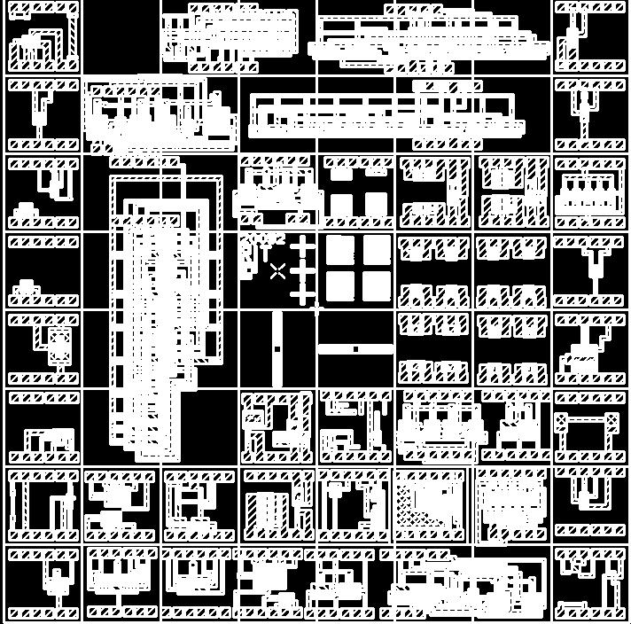
4 PMOS ES CHIP Page 4

5 ES FACILIY HP4145 Semiconductor Paramater Analyzer Keithley 7001 Switch Matrix Computer ICS Software Camera Ultracision Semi-Automatic Wafer Prober est Fixture and Manual Probe Station Page 5

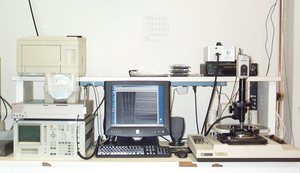
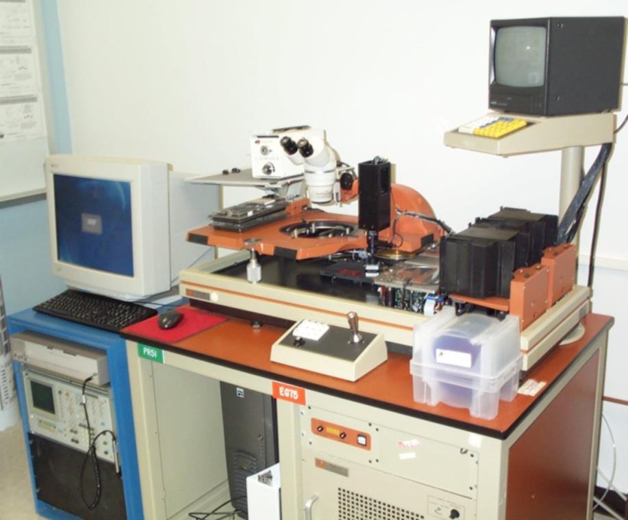
6 ES EQUIPMEN Semi-automatic Prober Automatic Prober Page 6

7 ES EQUIPMEN Manual Prober Page 7

8 RESISOR ES RESULS R = Rhos L/W L/W = 400/60 R = V/I = 1/slope = 647 W Page 8
9 VAN DER PAUW ES SRUCURES FOR SHEE RESISANCE I I Rs V1-V2 V1 V2 I I I Rs = (V1-V2) I ln 2 V1 V2 Page 9
10 VAN DER PAUW ES RESULS 26.4 Ohms Page 10

11 CBKR AND INVERERS Page 11
12 CROSS BRIDGE KELVIN RESISANCE ES SRUCURES FOR CONAC RESISANCES Gc V1-V2 V1 I W1 W2 V2 I I Rc = (V1-V2) I ohms Gc = I 1 (V1-V2) W1 x W2 mhos/µm 2 Page 12
 = (# defective x 1612) / (# tested) Page")
13 500 µm PMOS esting at RI MEAL AND DIFFUSION SERPENINE 100 µm Line width = 15 µm Line Space = 30 µm L/W = 269 Area Covered by metal = µm 2 R = Rhos L/W Defect density ( in #/cm 2 ) = (# defective x 1612) / (# tested) Page 13

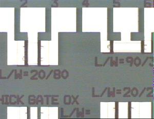
14 PMOS RANSISORS Layout Photograph Page 14

15 PMOS RANSISOR ES RESULS Vds + G Vgs - D S Id Page 15
16 RANSISOR LINEAR REGION V, GM + Vgs - -Id G gm S D Vto Id Vsub Vd = -0.1 Volt Vsub = 0 Body Effect Vsub volts -Vg gm = DId/DVg -Ids Non Saturation Region S p G Vsub pmosfe with Vt=-1, since the Drain is at -0.1 volts and the source is at zero. Both drain and source will be on at gate voltages greater than -1.1 volt. the transistor will be in the non saturation region. D p n Vgs -Vds Page 16

17 LINEAR REGION ES RESULS Page 17
18 RANSISOR SAURAION REGION V, GM -Id G S D gm Id Vto + Vgs=Vds - Vsub Vsub = volts -Vg gm = DId/DVg Body Effect PMOS -Ids S p Saturation Region -5-4 Vgs -3-2 G Vsub -Vds pmosfe with Vt=-1, Drain end is never on because Voltage Gate to Drain is Zero. herefore this transistor is always in Saturation Region if the gate voltage is above the threshold voltage. D p n Page 18
19 RANSISOR SUB HRESHOLD ID-VGS G S D Id + Vgs=Vds Id (Amps) Lights On Sub Vt Slope (mv/dec) Vgs Vt he subthreshold characteristics are important in VLSI circuits because when the transistors are off they should not carry much current since there are so many transistors. (typical value about 100 mv/decade) Page 19


20 INVERERS L = 40µm W = 20µm L = 20µm W = 50µm Page 20
21 INVERERS VIN Inverter Gain = VOU Wd/Ld Wu/Lu -V Voh VOU Slope = Gain -V VIN VOU VoL 0 0 ViL Vih -V VIN PMOS Inverter with Enhancement Load D 0 noise margin = ViL - Voh D 1 noise margin = Voh - Vih Page 21

22 INVERER ES RESULS Gain = Page 22
23 RING OSCILLAOR, td Seven stage ring oscillator with two output buffers td = / 2 N td = gate delay N = number of stages = period of oscillation Vout Vout = period of oscillation Page 23


24 9 SAGE RING OSCILLAOR Vcc Gnd Out Page 24

25 RING OSCILLAOR OUPU 500ns td = / 2n = 500 ns / 2 / 9 = 28 ns Page 25
26 DIGIAL CIRCUI ESING Page 26

27 LAB VIEW SOFWARE Page 27


28 HARDWARE FOR OUPU 6 Analog Outputs Ribbon Cable erminal Board Page 28


29 HARDWARE FOR INPU 16 Analog Inputs Ribbon Cable erminal Board Page 29

30 FINAL SYSEM Page 30

31 CUSOM SOFWARE INERFACE Click on digital testing icon to invoke the lab view software and this main menu. Click to select the type of test you wish to run. MAIN MENU Page 31


32 NOR GAE AND NOR FLIP FLOP PMOS 2 INPU NOR PMOS NOR RS Flip Flop Page 32

33 ESING WO INPU ONE OUPU LOGIC GAES Page 33
34 FOUR CHOICES FOR SUPPLY VOLAGES CLICK O SELEC ONE CMOS/L Vcc = +5 Volts Page 34


35 PROBE CARD/WIRE CONNECIONS Page 35

36 SWICH MARIX (MANUAL) Wire #17 Supply Outputs Vcc -V Gnd a b c d e f Inputs a b c d e f Wire #8 Page 36

37 RUN ES Click to Select When Output is High or Low Click to Start est Stop est est Results For Xor Gate Page 37


38 PMOS INVERER GAIN=4 Page 38


39 PMOS 2-INPU NOR est for PMOS wo Input NOR, Gain = 4 or 8 Page 39


40 PMOS 2-INPU XOR Page 40
41 WAFER MAPS FOR MESA nmos Vt target Row 1 Row 15 Col 1 Col 15 row 1 is the first row in which a full die is located column 1 is the first column in which a full die is locatedd Page 41
42 WAFER MAPS FOR MESA Code 0 no die 1 value<(arget-40%) 2 (arget-40%)<value<(arget-30%) 3 (arget-30%)<value<(arget-20%) 4 (arget-20%)<value<(arget-10%) 5 (arget-10%)<value<(arget+10%) 6 (arget+10%)<value<(arget+20%) 7 (arget+20%)<value<(arget+30%) 8 (arget+30%)<value<(arget+40%) 9 (arget+40%)<value Page 42

43 WAFER MAP Example: Given a wafer with test chips located as shown and nmos threshold voltage data encoded and stored in MESA as shown. Reconstruct a wafer map using EXCELL spreadsheet. Page 43
44 FUURE WORK More Automation Improved Wafer Mapping More Complete esting Page 44
45 CONCLUSION A test specification has been developed A history data base has been developed esting is very time consuming. It takes us 9 hours to do all the specified tests and even then we only test a few devices on a wafer. Currently we test about 1% of the devices Page 45
46 REFERENCES 1. LabView Software, National Instruments, Page 46
47 REVIEW QUESIONS - PMOS ES SPECIFICAION 1. How is Vt and gm found from the transistor family of curves. 2. Is the Vt and gm the same in the non-saturation region as in the saturation region? 3. What is the significance of the sub-threshold slope. What is the difference between sub-threshold slope and subthreshold swing? 4. What is the significance of the noise margin. 5. What is the purpose of the ring oscillator test structure. Page 47

48 MUX LAYOU AND GAE LEVEL SCHEMAIC 25 ransistors I 0 A A A B I 0 I 1 A BI 1 Q I 2 I 3 B B AB I 2 ABI 3 Page 48

49 PMOS 4-INPU MULIPLEXER Page 49


50 MUX ES RESULS A B I3 I2 I1 I0 A B I3 I2 I1 I0 In PMOS logic low is 0 volts, logic high is -Vcc A B I3 I2 I1 I0 A B I3 I2 I1 I0 Page 50


51 MUX ES RESULS A B I3 I2 I1 I0 A B I3 I2 I1 I0 In PMOS logic low is 0 volts, logic high is -Vcc A B I3 I2 I1 I0 A B I3 I2 I1 I0 Page 51

52 PMOS FULL ADDER Page 52

53 PMOS CLOCKED DAA LACH Page 53

54 PMOS ANALOG MUX Page 54
PMOS Digital Testing at Rochester Institute of Technology
 1 PMOS Digital Testing at Rochester Institute of Technology Dr. Lynn Fuller, Adam Wardas webpage: http://www.rit.edu/lffeee Microelectronic Engineering Rochester Institute of Technology 82 Lomb Memorial
Introduction to the Long Channel MOSFET. Dr. Lynn Fuller
 ROCHESTER INSTITUTE OF TECHNOLOGY MICROELECTRONIC ENGINEERING Introduction to the Long Channel MOSFET Dr. Lynn Fuller Webpage: http://people.rit.edu/lffeee Electrical and 82 Lomb Memorial Drive Rochester,
MOS Inverters Dr. Lynn Fuller Webpage:
 ROCHESTER INSTITUTE OF TECHNOLOGY MICROELECTRONIC ENGINEERING MOS Inverters Webpage: http://people.rit.edu/lffeee 82 Lomb Memorial Drive Rochester, NY 14623-5604 Tel (585) 475-2035 Email: Lynn.Fuller@rit.edu
DIGITAL VLSI LAB ASSIGNMENT 1
 DIGITAL VLSI LAB ASSIGNMENT 1 Problem 1: NMOS and PMOS plots using Cadence. In this exercise, you are required to generate both NMOS and PMOS I-V device characteristics (I/P and O/P) using Cadence (Use
BJT Characterization Laboratory Dr. Lynn Fuller
 ROCHESTER INSTITUTE OF TECHNOLOGY MICROELECTRONIC ENGINEERING BJT Characterization Laboratory Dr. Lynn Fuller 82 Lomb Memorial Drive Rochester, NY 14623-5604 Tel (585) 475-2035 Fax (585) 475-5041 Email:
Advanced MOSFET Basics. Dr. Lynn Fuller
 ROCHESTER INSTITUTE OF TECHNOLOGY MICROELECTRONIC ENGINEERING Advanced MOSFET Basics Dr. Lynn Fuller Webpage: http://people.rit.edu/lffeee 82 Lomb Memorial Drive Rochester, NY 14623-5604 Tel (585) 475-2035
NMOS Inverter Lab ROCHESTER INSTITUTE OF TECHNOLOGY MICROELECTRONIC ENGINEERING. NMOS Inverter Lab
 ROCHESTER INSTITUTE OF TECHNOLOGY MICROELECTRONIC ENGINEERING NMOS Inverter Lab Dr. Lynn Fuller Webpage: http://people.rit.edu/lffeee/ 82 Lomb Memorial Drive Rochester, NY 14623-5604 Tel (585) 475-2035
Embedded Systems. Oscillator and I/O Hardware. Eng. Anis Nazer First Semester
 Embedded Systems Oscillator and I/O Hardware Eng. Anis Nazer First Semester 2016-2017 Oscillator configurations Three possible configurations for Oscillator (a) using a crystal oscillator (b) using an
Static Random Access Memory - SRAM Dr. Lynn Fuller Webpage:
 ROCHESTER INSTITUTE OF TECHNOLOGY MICROELECTRONIC ENGINEERING Static Random Access Memory - SRAM Dr. Lynn Fuller Webpage: http://people.rit.edu/lffeee 82 Lomb Memorial Drive Rochester, NY 14623-5604 Email:
Differential Amplifier with Current Source Bias and Active Load
 Technical Memo: Differential Amplifier with Current Source Bias and Active Load Introduction: From: Dr. Lynn Fuller, Professor, Electrical and Microelectronic Engineering, Rochester Institute of Technology
Logic Controlled, High-Side Power Switches ADP190/ADP191
 Logic Controlled, High-Side Power Switches FEAURES Low RDSON of 5 mω at.8 V Internal output discharge resistor (ADP9) urn-on slew rate limiting (ADP9) Low input voltage range:. V to 3.6 V 5 ma continuous
ECE2274 Pre-Lab for MOSFET logic LTspice NAND Gate, NOR Gate, and CMOS Inverter
 ECE2274 Pre-Lab for MOFET logic LTspice NAN ate, NOR ate, and CMO Inverter 1. NMO NAN ate Use Vdd = 9.. For the NMO NAN gate shown below gate, using the 2N7000 MOFET LTspice model such that Vto = 2.0.
ELEC 2210 EXPERIMENT 12 NMOS Logic
 ELEC 2210 EXPERIMENT 12 NMOS Logic Objectives: The experiments in this laboratory exercise will provide an introduction to NMOS logic. You will use the Bit Bucket breadboarding system to build and test
ENEE307 Lab 7 MOS Transistors 2: Small Signal Amplifiers and Digital Circuits
 ENEE307 Lab 7 MOS Transistors 2: Small Signal Amplifiers and Digital Circuits In this lab, we will be looking at ac signals with MOSFET circuits and digital electronics. The experiments will be performed
4-bit counter circa bit counter circa 1990
 Digital Logic 4-bit counter circa 1960 8-bit counter circa 1990 Logic gates Operates on logical values (TRUE = 1, FALSE = 0) NOT AND OR XOR 0-1 1-0 0 0 0 1 0 0 0 1 0 1 1 1 0 0 0 1 0 1 0 1 1 1 1 1 0 0 0
EE 230 Lab Lab 9. Prior to Lab
 MOS transistor characteristics This week we look at some MOS transistor characteristics and circuits. Most of the measurements will be done with our usual lab equipment, but we will also use the parameter
Advanced MOSFET Basics. Dr. Lynn Fuller
 ROCHESTER INSTITUTE OF TECHNOLOGY MICROELECTRONIC ENGINEERING Advanced MOSFET Basics Dr. Lynn Fuller Webpage: http://people.rit.edu/lffeee 82 Lomb Memorial Drive Rochester, NY 14623-5604 Tel (585) 475-2035
Introduction to VLSI ASIC Design and Technology
 Introduction to VLSI ASIC Design and Technology Paulo Moreira CERN - Geneva, Switzerland Paulo Moreira Introduction 1 Outline Introduction Is there a limit? Transistors CMOS building blocks Parasitics
ECSE 6300 IC Fabrication Laboratory Lecture 10 Device Characterization. Die Image
 ECSE 6300 IC Fabrication Laboratory Lecture 10 Device Characterization Prof. Bldg. CII, Rooms 6229 Rensselaer Polytechnic Institute Troy, NY 12180 Tel. (518)276-2909 e-mails: luj@rpi.edu http://www.ecse.rpi.edu/courses/s18/ecse
Design cycle for MEMS
 Design cycle for MEMS Design cycle for ICs IC Process Selection nmos CMOS BiCMOS ECL for logic for I/O and driver circuit for critical high speed parts of the system The Real Estate of a Wafer MOS Transistor
Introduction to Electronics. Dr. Lynn Fuller
 ROCHESTER INSTITUTE OF TECHNOLOGY MICROELECTRONIC ENGINEERING Introduction to Electronics Dr. Lynn Fuller Webpage: http://www.rit.edu/~lffeee 82 Lomb Memorial Drive Rochester, NY 14623-5604 Tel (585) 475-2035
3. COMPARING STRUCTURE OF SINGLE GATE AND DOUBLE GATE MOSFET WITH DESIGN AND CURVE
 P a g e 80 Available online at http://arjournal.org APPLIED RESEARCH JOURNAL RESEARCH ARTICLE ISSN: 2423-4796 Applied Research Journal Vol. 3, Issue, 2, pp.80-86, February, 2017 COMPARATIVE STUDY ON SINGLE
Place answers on the supplied BUBBLE SHEET only nothing written here will be graded.
 ECE 270 Learning Outcome 1-1 - Practice Exam B OUTCOME #1: an ability to analyze and design CMOS logic gates. Multiple Choice select the single most appropriate response for each question. Note that none
MOS TRANSISTOR THEORY
 MOS TRANSISTOR THEORY Introduction A MOS transistor is a majority-carrier device, in which the current in a conducting channel between the source and the drain is modulated by a voltage applied to the
Transistor was first invented by William.B.Shockley, Walter Brattain and John Bardeen of Bell Labratories. In 1961, first IC was introduced.
 Unit 1 Basic MOS Technology Transistor was first invented by William.B.Shockley, Walter Brattain and John Bardeen of Bell Labratories. In 1961, first IC was introduced. Levels of Integration:- i) SSI:-
4-bit counter circa bit counter circa 1990
 Digital Logic 4-bit counter circa 1960 8-bit counter circa 1990 Logic gates Operates on logical values (TRUE = 1, FALSE = 0) NOT AND OR XOR 0-1 1-0 0 0 0 1 0 0 0 1 0 1 1 1 0 0 0 1 0 1 0 1 1 1 1 1 0 0 0
TECHNO INDIA BATANAGAR (DEPARTMENT OF ELECTRONICS & COMMUNICATION ENGINEERING) QUESTION BANK- 2018
 QUESTION BANK- 2018") TECHNO INDIA BATANAGAR (DEPARTMENT OF ELECTRONICS & COMMUNICATION ENGINEERING) QUESTION BANK- 2018 Paper Setter Detail Name Designation Mobile No. E-mail ID Raina Modak Assistant Professor 6290025725 raina.modak@tib.edu.in
TECHNO INDIA BATANAGAR (DEPARTMENT OF ELECTRONICS & COMMUNICATION ENGINEERING) QUESTION BANK- 2018 Paper Setter Detail Name Designation Mobile No. E-mail ID Raina Modak Assistant Professor 6290025725 raina.modak@tib.edu.in
Synchronization of single-channel stepper motor drivers reduces noise and interference
 hronizaion of single-channel sepper moor drivers reduces noise and inerference n mos applicaions, a non-synchronized operaion causes no problems. However, in some cases he swiching of he wo channels inerfere,
Reading. Lecture 17: MOS transistors digital. Context. Digital techniques:
 Reading Lecture 17: MOS transistors digital Today we are going to look at the analog characteristics of simple digital devices, 5. 5.4 And following the midterm, we will cover PN diodes again in forward
Lecture 13. Biasing and Loading Single Stage FET Amplifiers. The Building Blocks of Analog Circuits - III
 Lecture 3 Biasing and Loading Single Stage FET Amplifiers The Building Blocks of Analog Circuits III In this lecture you will learn: Current biasing of circuits Current sources and sinks for CS, CG, and
COLLECTOR DRAIN BASE GATE EMITTER. Applying a voltage to the Gate connection allows current to flow between the Drain and Source connections.
 MOSFETS Although the base current in a transistor is usually small (< 0.1 ma), some input devices (e.g. a crystal microphone) may be limited in their output. In order to overcome this, a Field Effect Transistor
ESE370: Circuit-Level Modeling, Design, and Optimization for Digital Systems. Today. Two Problems. Outline. Output not go to Rail
 ESE370: Circuit-Level Modeling, Design, and Optimization for Digital Systems Day 6: September 19, 2011 Restoration Today How do we make sure logic is robust Can assemble into any (feed forward) graph Can
Unit III FET and its Applications. 2 Marks Questions and Answers
 Unit III FET and its Applications 2 Marks Questions and Answers 1. Why do you call FET as field effect transistor? The name field effect is derived from the fact that the current is controlled by an electric
ESE370: Circuit-Level Modeling, Design, and Optimization for Digital Systems. Today. Two Problems. Outline. Output not go to Rail
 ESE370: Circuit-Level Modeling, Design, and Optimization for Digital Systems Day 6: September 17, 2012 Restoration Today How do we make sure logic is robust Can assemble into any (feed forward) graph Can
High Voltage and MEMS Process Integration
 ROCHESTER INSTITUTE OF TECHNOLOGY MICROELECTRONIC ENGINEERING High Voltage and MEMS Process Integration Dr. Lynn Fuller and Dr. Ivan Puchades webpage: http://people.rit.edu/lffeee Electrical and Microelectronic
CD40174BMS. CMOS Hex D -Type Flip-Flop. Features. Pinout. Applications. Functional Diagram. Description. December 1992
 SEMICONDUCTOR CD17BMS December 199 CMOS Hex D -Type Flip-Flop Features Pinout High Voltage Type (V Rating) 5V, and 15V Parametric Ratings CD17BMS TOP VIEW Standardized, Symmetrical Output Characteristics
Curve Tracer Laboratory Assistant Using the Analog Discovery Module as A Curve Tracer
 Curve Tracer Laboratory Assistant Using the Analog Discovery Module as A Curve Tracer The objective of this lab is to become familiar with methods to measure the dc current-voltage (IV) behavior of diodes
EECS150 - Digital Design Lecture 19 CMOS Implementation Technologies. Recap and Outline
 EECS150 - Digital Design Lecture 19 CMOS Implementation Technologies Oct. 31, 2013 Prof. Ronald Fearing Electrical Engineering and Computer Sciences University of California, Berkeley (slides courtesy
EXPERIMENT # 1: REVERSE ENGINEERING OF INTEGRATED CIRCUITS Week of 1/17/05
 EXPERIMENT # 1: REVERSE ENGINEERING OF INTEGRATED CIRCUITS Week of 1/17/5 Experiment #1: Reading: Reverse engineering of integrated circuits Jaeger 9.2: MOS transistor layout and design rules HP4145 basics:
Lab 2 Revisited Exercise
 Lab 2 Revisited Exercise +15V 100k 1K 2N2222 Wire up led display Note the ground leads LED orientation 6.091 IAP 2008 Lecture 3 1 Comparator, Oscillator +5 +15 1k 2 V- 7 6 Vin 3 V+ 4 V o Notice that power
EE584 Introduction to VLSI Design Final Project Document Group 9 Ring Oscillator with Frequency selector
 EE584 Introduction to VLSI Design Final Project Document Group 9 Ring Oscillator with Frequency selector Group Members Uttam Kumar Boda Rajesh Tenukuntla Mohammad M Iftakhar Srikanth Yanamanagandla 1 Table
DATASHEET CD4069UBMS. Features. Pinout. Applications. Functional Diagram. Description. Schematic Diagram. CMOS Hex Inverter
 DATASHEET CD9UBMS CMOS Hex Inverter FN331 Rev. December 199 Features Pinout High Voltage Types (V Rating) Standardized Symmetrical Output Characteristics CD9UBMS TOP VIEW Medium Speed Operation: tphl,
NXP. P5CC052 Secure Contact PKI Smart Card Controller. Analog Circuit Analysis
 NXP P5CC052 Secure Contact PKI Smart Card Controller Analog Circuit Analysis 3685 Richmond Road, Suite 500, Ottawa, ON K2H 5B7 Canada Tel: 613.829.0414 Fax: 613.829.0515 www.chipworks.com Some of the information
Solution HW4 Dr. Parker EE477
 Solution HW4 Dr. Parker EE477 Assume for the problems below that V dd = 1.8 v, V tp0 is -.7 v. and V tn0 is.7 V. V tpbodyeffect is -.9 v. and V tnbodyeffect is.9 V. Assume ß n (k n )= 219.4 W/L µ A(microamps)/V
ECEN3250 Lab 9 CMOS Logic Inverter
 Lab 9 CMOS Logic Inverter ECE Department University of Colorado, Boulder 1 Prelab Read Section 4.10 (4th edition Section 5.8), and the Lab procedure Do and turn in Exercise 4.41 (page 342) Do PSpice (.dc)
ECE 5745 Complex Digital ASIC Design Topic 2: CMOS Devices
 ECE 5745 Complex Digital ASIC Design Topic 2: CMOS Devices Christopher Batten School of Electrical and Computer Engineering Cornell University http://www.csl.cornell.edu/courses/ece5950 Simple Transistor
ENGR 210 Lab 12: Analog to Digital Conversion
 ENGR 210 Lab 12: Analog to Digital Conversion In this lab you will investigate the operation and quantization effects of an A/D and D/A converter. A. BACKGROUND 1. LED Displays We have been using LEDs
55:041 Electronic Circuits
 55:041 Electronic Circuits MOSFETs Sections of Chapter 3 &4 A. Kruger MOSFETs, Page-1 Basic Structure of MOS Capacitor Sect. 3.1 Width = 1 10-6 m or less Thickness = 50 10-9 m or less ` MOS Metal-Oxide-Semiconductor
DATASHEET CD4060BMS. Pinout. Features. Functional Diagram. Oscillator Features. Applications. Description
 DATASHEET CDBMS CMOS 1 Stage Ripple-Carry Binary Counter/Divider and Oscillator FN3317 Rev. Features Pinout High Voltage Type (V Rating) Common Reset 1MHz Clock Rate at 15V Fully Static Operation Q1 Q13
Introduction. Digital Integrated Circuits A Design Perspective. Jan M. Rabaey Anantha Chandrakasan Borivoje Nikolic. July 30, 2002
 Digital Integrated Circuits A Design Perspective Jan M. Rabaey Anantha Chandrakasan Borivoje Nikolic Introduction July 30, 2002 1 What is this book all about? Introduction to digital integrated circuits.
Digital Design and System Implementation. Overview of Physical Implementations
 Digital Design and System Implementation Overview of Physical Implementations CMOS devices CMOS transistor circuit functional behavior Basic logic gates Transmission gates Tri-state buffers Flip-flops
Diode Sensor Lab. Dr. Lynn Fuller
 ROCHESTER INSTITUTE OF TECHNOLOGY MICROELECTRONIC ENGINEERING Diode Sensor Lab Dr. Lynn Fuller Webpage: http://people.rit.edu/lffeee 82 Lomb Memorial Drive Rochester, NY 14623-5604 Tel (585) 475-2035 Fax
PC accounts for 353 Cory will be created early next week (when the class list is completed) Discussions & Labs start in Week 3
 Discussions & Labs start in Week 3") EE141 Fall 2005 Lecture 2 Design Metrics Admin Page Everyone should have a UNIX account on Cory! This will allow you to run HSPICE! If you do not have an account, check: http://www-inst.eecs.berkeley.edu/usr/
EE141 Fall 2005 Lecture 2 Design Metrics Admin Page Everyone should have a UNIX account on Cory! This will allow you to run HSPICE! If you do not have an account, check: http://www-inst.eecs.berkeley.edu/usr/
ENEE 307 Laboratory#2 (n-mosfet, p-mosfet, and a single n-mosfet amplifier in the common source configuration)
") Revised 2/16/2007 ENEE 307 Laboratory#2 (n-mosfet, p-mosfet, and a single n-mosfet amplifier in the common source configuration) *NOTE: The text mentioned below refers to the Sedra/Smith, 5th edition.
Revised 2/16/2007 ENEE 307 Laboratory#2 (n-mosfet, p-mosfet, and a single n-mosfet amplifier in the common source configuration) *NOTE: The text mentioned below refers to the Sedra/Smith, 5th edition.
Lecture Integrated circuits era
 Lecture 1 1.1 Integrated circuits era Transistor was first invented by William.B.Shockley, Walter Brattain and John Bardeen of Bell laboratories. In 1961, first IC was introduced. Levels of Integration:-
EEC 216 Lecture #10: Ultra Low Voltage and Subthreshold Circuit Design. Rajeevan Amirtharajah University of California, Davis
 EEC 216 Lecture #1: Ultra Low Voltage and Subthreshold Circuit Design Rajeevan Amirtharajah University of California, Davis Opportunities for Ultra Low Voltage Battery Operated and Mobile Systems Wireless
Introduction to LTSPICE Dr. Lynn Fuller Electrical and Microelectronic Engineering
 ROCHESTER INSTITUTE OF TECHNOLOGY MICROELECTRONIC ENGINEERING Introduction to LTSPICE Dr. Lynn Fuller Electrical and 82 Lomb Memorial Drive Rochester, NY 14623-5604 Tel (585) 475-2035 Fax (585) 475-5041
EE 330 Laboratory 7 MOSFET Device Experimental Characterization and Basic Applications Spring 2017
 EE 330 Laboratory 7 MOSFET Device Experimental Characterization and Basic Applications Spring 2017 Objective: The objective of this laboratory experiment is to become more familiar with the operation of
ECE 2274 MOSFET Voltmeter. Richard Cooper
 ECE 2274 MOSFET Voltmeter Richard Cooper Pre-Lab for MOSFET Voltmeter Voltmeter design: Build a MOSFET (2N7000) voltmeter in LTspice. The MOSFETs in the voltmeter act as switches. To turn on the MOSFET.
ENSC 495/851 Lab Electrical and Device Measurements V1.0 Mar Glenn Chapman
 ENSC 495/851 Lab Electrical and Device Measurements V1.0 Mar. 25 2015 Glenn Chapman Testing the devices is done after level 4 has been completed and wafers ENSC 495 students will do at least parts 1 to
0.85V. 2. vs. I W / L
 EE501 Lab3 Exploring Transistor Characteristics and Design Common-Source Amplifiers Lab report due on September 22, 2016 Objectives: 1. Be familiar with characteristics of MOSFET such as gain, speed, power,
To design/build monostable multivibrators using 555 IC and verify their operation using measurements by observing waveforms.
 AIM: SUBJECT: ANALOG ELECTRONICS (2130902) EXPERIMENT NO. 09 DATE : TITLE: TO DESIGN/BUILD MONOSTABLE MULTIVIBRATORS USING 555 IC AND VERIFY THEIR OPERATION USING MEASUREMENTS BY OBSERVING WAVEFORMS. DOC.
1. Short answer questions. (30) a. What impact does increasing the length of a transistor have on power and delay? Why? (6)
 a. What impact does increasing the length of a transistor have on power and delay? Why? (6)") CSE 493/593 Test 2 Fall 2011 Solution 1. Short answer questions. (30) a. What impact does increasing the length of a transistor have on power and delay? Why? (6) Decreasing of W to make the gate slower,
CSE 493/593 Test 2 Fall 2011 Solution 1. Short answer questions. (30) a. What impact does increasing the length of a transistor have on power and delay? Why? (6) Decreasing of W to make the gate slower,
Power Conditioning Electronics Dr. Lynn Fuller Webpage:
 ROCHESTER INSTITUTE OF TECHNOLOGY MICROELECTRONIC ENGINEERING Power Conditioning Electronics Dr. Lynn Fuller Webpage: http://people.rit.edu/lffeee 82 Lomb Memorial Drive Rochester, NY 14623-5604 Email:
Field Effect Transistors
 Field Effect Transistors LECTURE NO. - 41 Field Effect Transistors www.mycsvtunotes.in JFET MOSFET CMOS Field Effect transistors - FETs First, why are we using still another transistor? BJTs had a small
Digital Microelectronic Circuits ( ) Pass Transistor Logic. Lecture 9: Presented by: Adam Teman
 Pass Transistor Logic. Lecture 9: Presented by: Adam Teman") Digital Microelectronic Circuits (361-1-3021 ) Presented by: Adam Teman Lecture 9: Pass Transistor Logic 1 Motivation In the previous lectures, we learned about Standard CMOS Digital Logic design. CMOS
Digital Microelectronic Circuits (361-1-3021 ) Presented by: Adam Teman Lecture 9: Pass Transistor Logic 1 Motivation In the previous lectures, we learned about Standard CMOS Digital Logic design. CMOS
LSI/CSI LS7560N LS7561N BRUSHLESS DC MOTOR CONTROLLER
 LSI/CSI LS7560N LS7561N LSI Computer Systems, Inc. 15 Walt Whitman Road, Melville, NY 747 (631) 71-0400 FAX (631) 71-0405 UL A3800 BRUSHLESS DC MOTOR CONTROLLER April 01 FEATURES Open loop motor control
Lecture 4. The CMOS Inverter. DC Transfer Curve: Load line. DC Operation: Voltage Transfer Characteristic. Noise in Digital Integrated Circuits
 Noise in Digital Integrated Circuits Lecture 4 The CMOS Inverter i(t) v(t) V DD Peter Cheung Department of Electrical & Electronic Engineering Imperial College London URL: www.ee.ic.ac.uk/pcheung/ E-mail:
VLSI Design I; A. Milenkovic 1
 CPE/EE 427, CPE 527 VLSI Design I L02: Design Metrics Department of Electrical and Computer Engineering University of Alabama in Huntsville Aleksandar Milenkovic ( www.ece.uah.edu/~milenka ) www.ece.uah.edu/~milenka/cpe527-03f
The Design and Realization of Basic nmos Digital Devices
 Proceedings of The National Conference On Undergraduate Research (NCUR) 2004 Indiana University Purdue University Indianapolis, Indiana April 15-17, 2004 The Design and Realization of Basic nmos Digital
Intelligent Systems Group Department of Electronics. An Evolvable, Field-Programmable Full Custom Analogue Transistor Array (FPTA)
") Department of Electronics n Evolvable, Field-Programmable Full Custom nalogue Transistor rray (FPT) Outline What`s Behind nalog? Evolution Substrate custom made configurable transistor array (FPT) Ways
Department of Electronics n Evolvable, Field-Programmable Full Custom nalogue Transistor rray (FPT) Outline What`s Behind nalog? Evolution Substrate custom made configurable transistor array (FPT) Ways
Note that none of the above MAY be a VALID ANSWER.
 ECE 270 Learning Outcome 1-1 - Practice Exam / Solution LEARNING OUTCOME #1: an ability to analyze and design CMOS logic gates. Multiple Choice select the single most appropriate response for each question.
Potato IC. Contact Potato Semiconductor for IP or detail. PotatoSemi High frequency noise cancellation technology.
 How oes PoaoSemi Kill inside Of I? Volage mode differenial Logic. New Paen IP. d MOS logic by using high frequency noise cancellaion echnology Poao I Normal I 2 1 20 19 Inpu1 Inpu2 Inpu3 ie Oupu1 Oupu2
PMOS OPERATIONAL AMPLIFIER. Khanh-Biflh Ta 5th Year Microelectronic Engineering Student Rochester Institute of TechnolOgy ABSTRACT
 PMOS OPERATIONAL AMPLIFIER Khanh-Biflh Ta 5th Year Microelectronic Engineering Student Rochester Institute of TechnolOgy ABSTRACT This project was characteristics. an Due evaluation of to nonworking a
Obsolete Product(s) - Obsolete Product(s)
 - Obsolete Product(s)") DUAL SWITCH-MODE SOLENOID DRIER HIGH CURRENT CAPABILITY (up o.5a per channel) HIGH OLTAGE OPERATI (up o 46 for power sage) HIGH EFFICIENCY SWITCHMODE OPERATI REGULATED OUTPUT CURRENT (adjusable) FEW EXTERNAL
DUAL SWITCH-MODE SOLENOID DRIER HIGH CURRENT CAPABILITY (up o.5a per channel) HIGH OLTAGE OPERATI (up o 46 for power sage) HIGH EFFICIENCY SWITCHMODE OPERATI REGULATED OUTPUT CURRENT (adjusable) FEW EXTERNAL
DESIGN OF A 4-BiT PMOS PARALLEL COMPARATOR AID CONVERTER. Amel Gaddo 5th year Microelectronic Engineering Student Rochester Institute of TechnologY
 DESIGN OF A 4-BiT PMOS PARALLEL COMPARATOR AID CONVERTER Amel Gaddo 5th year Microelectronic Engineering Student Rochester Institute of TechnologY ABSTRACT INTRODUCTION This project dealt with the design
A Low Power Array Multiplier Design using Modified Gate Diffusion Input (GDI)
") A Low Power Array Multiplier Design using Modified Gate Diffusion Input (GDI) Mahendra Kumar Lariya 1, D. K. Mishra 2 1 M.Tech, Electronics and instrumentation Engineering, Shri G. S. Institute of Technology
A Low Power Array Multiplier Design using Modified Gate Diffusion Input (GDI) Mahendra Kumar Lariya 1, D. K. Mishra 2 1 M.Tech, Electronics and instrumentation Engineering, Shri G. S. Institute of Technology
UNIVERSITY OF NORTH CAROLINA AT CHARLOTTE Department of Electrical and Computer Engineering
 UNIVERSITY OF NORTH CAROLINA AT CHARLOTTE Department of Electrical and Computer Engineering EXPERIMENT 8 MOSFET AMPLIFIER CONFIGURATIONS AND INPUT/OUTPUT IMPEDANCE OBJECTIVES The purpose of this experiment
Combinational Logic. Prof. MacDonald
 Combinational Logic Prof. MacDonald 2 Input NOR depletion NFET load l Pull Down Network can pull OUT down if either or both inputs are above Vih consequently the NOR function. l Depletion NFET could really
Module-3: Metal Oxide Semiconductor (MOS) & Emitter coupled logic (ECL) families
 & Emitter coupled logic (ECL) families") 1 Module-3: Metal Oxide Semiconductor (MOS) & Emitter coupled logic (ECL) families 1. Introduction 2. Metal Oxide Semiconductor (MOS) logic 2.1. Enhancement and depletion mode 2.2. NMOS and PMOS inverter
1 Module-3: Metal Oxide Semiconductor (MOS) & Emitter coupled logic (ECL) families 1. Introduction 2. Metal Oxide Semiconductor (MOS) logic 2.1. Enhancement and depletion mode 2.2. NMOS and PMOS inverter
Why Scaling? CPU speed Chip size R, C CPU can increase speed by reducing occupying area.
 Why Scaling? Higher density : Integration of more transistors onto a smaller chip : reducing the occupying area and production cost Higher Performance : Higher current drive : smaller metal to metal capacitance
Combinational Logic Gates in CMOS
 Combinational Logic Gates in CMOS References: dapted from: Digital Integrated Circuits: Design Perspective, J. Rabaey UC Principles of CMOS VLSI Design: Systems Perspective, 2nd Ed., N. H. E. Weste and
GUJARAT TECHNOLOGICAL UNIVERSITY. Semester II. Type of course: ME-Electronics & Communication Engineering (VLSI & Embedded Systems Design)
") GUJARAT TECHNOLOGICAL UNIVERSITY Subject Name: Analog and Mixed Signal IC Design (Elective) Subject Code: 3725206 Semester II Type of course: ME-Electronics & Communication Engineering (VLSI & Embedded
GUJARAT TECHNOLOGICAL UNIVERSITY Subject Name: Analog and Mixed Signal IC Design (Elective) Subject Code: 3725206 Semester II Type of course: ME-Electronics & Communication Engineering (VLSI & Embedded
Shorthand Notation for NMOS and PMOS Transistors
 Shorthand Notation for NMOS and PMOS Transistors Terminal Voltages Mode of operation depends on V g, V d, V s V gs = V g V s V gd = V g V d V ds = V d V s = V gs - V gd Source and drain are symmetric diffusion
EECS150 - Digital Design Lecture 15 - CMOS Implementation Technologies. Overview of Physical Implementations
 EECS150 - Digital Design Lecture 15 - CMOS Implementation Technologies Mar 12, 2013 John Wawrzynek Spring 2013 EECS150 - Lec15-CMOS Page 1 Overview of Physical Implementations Integrated Circuits (ICs)
EECS150 - Digital Design Lecture 9 - CMOS Implementation Technologies
 EECS150 - Digital Design Lecture 9 - CMOS Implementation Technologies Feb 14, 2012 John Wawrzynek Spring 2012 EECS150 - Lec09-CMOS Page 1 Overview of Physical Implementations Integrated Circuits (ICs)
This Week s Subject. DRAM & Flexible RRAM. p-channel MOSFET (PMOS) CMOS: Complementary Metal Oxide Semiconductor
 CMOS: Complementary Metal Oxide Semiconductor") DRAM & Flexible RRAM This Week s Subject p-channel MOSFET (PMOS) CMOS: Complementary Metal Oxide Semiconductor CMOS Logic Inverter NAND gate NOR gate CMOS Integration & Layout GaAs MESFET (JFET) 1 Flexible
DRAM & Flexible RRAM This Week s Subject p-channel MOSFET (PMOS) CMOS: Complementary Metal Oxide Semiconductor CMOS Logic Inverter NAND gate NOR gate CMOS Integration & Layout GaAs MESFET (JFET) 1 Flexible
Design of Low-Power High-Performance 2-4 and 4-16 Mixed-Logic Line Decoders
 Design of Low-Power High-Performance 2-4 and 4-16 Mixed-Logic Line Decoders B. Madhuri Dr.R. Prabhakar, M.Tech, Ph.D. bmadhusingh16@gmail.com rpr612@gmail.com M.Tech (VLSI&Embedded System Design) Vice
2009 Spring CS211 Digital Systems & Lab 1 CHAPTER 3: TECHNOLOGY (PART 2)
") 1 CHAPTER 3: IMPLEMENTATION TECHNOLOGY (PART 2) Whatwillwelearninthischapter? we learn in this 2 How transistors operate and form simple switches CMOS logic gates IC technology FPGAs and other PLDs Basic
1 CHAPTER 3: IMPLEMENTATION TECHNOLOGY (PART 2) Whatwillwelearninthischapter? we learn in this 2 How transistors operate and form simple switches CMOS logic gates IC technology FPGAs and other PLDs Basic
EE 40 Final Project Basic Circuit
 EE 0 Spring 2006 Final Projec EE 0 Final Projec Basic Circui Par I: General insrucion 1. The final projec will coun 0% of he lab grading, since i s going o ake lab sessions. All oher individual labs will
Logic Families. Describes Process used to implement devices Input and output structure of the device. Four general categories.
 Logic Families Characterizing Digital ICs Digital ICs characterized several ways Circuit Complexity Gives measure of number of transistors or gates Within single package Four general categories SSI - Small
A COMPARATIVE ANALYSIS OF 180 NM PROCESS CMOS INVERTER
 A COMPARATIVE ANALYSIS OF 180 NM PROCESS CMOS INVERTER Amresh Kumar Lenka Department of Electronics and Communication Engineering Centre for Advance Post Graduate Studies, Rourkela Ananya Dastidar Biju
Lecture 11 Circuits numériques (I) L'inverseur
 L'inverseur") Lecture 11 Circuits numériques (I) L'inverseur Outline Introduction to digital circuits The inverter NMOS inverter with resistor pull-up 6.12 Spring 24 Lecture 11 1 1. Introduction to digital circuits:
Lecture 11 Circuits numériques (I) L'inverseur Outline Introduction to digital circuits The inverter NMOS inverter with resistor pull-up 6.12 Spring 24 Lecture 11 1 1. Introduction to digital circuits:
Lecture 12 - Digital Circuits (I) The inverter. October 20, 2005
 The inverter. October 20, 2005") 6.12 - Microelectronic Devices and Circuits - Fall 25 Lecture 12-1 Lecture 12 - Digital Circuits (I) The inverter October 2, 25 Contents: 1. Introduction to digital electronics: the inverter 2. NMOS inverter
6.12 - Microelectronic Devices and Circuits - Fall 25 Lecture 12-1 Lecture 12 - Digital Circuits (I) The inverter October 2, 25 Contents: 1. Introduction to digital electronics: the inverter 2. NMOS inverter
12-nm Novel Topologies of LPHP: Low-Power High- Performance 2 4 and 4 16 Mixed-Logic Line Decoders
 12-nm Novel Topologies of LPHP: Low-Power High- Performance 2 4 and 4 16 Mixed-Logic Line Decoders Mr.Devanaboina Ramu, M.tech Dept. of Electronics and Communication Engineering Sri Vasavi Institute of
DATASHEET CD4027BMS. Features. Pinout. Functional Diagram. Applications. Description. CMOS Dual J-KMaster-Slave Flip-Flop. FN3302 Rev 0.
 DATASHEET CD7BMS CMOS Dual J-KMaster-Slave Flip-Flop FN33 Rev. Features Pinout High Voltage Type (V Rating) Set - Reset Capability CD7BMS TOP VIEW Static Flip-Flop Operation - Retains State Indefinitely
Field Effect Transistors (FET s) University of Connecticut 136
 University of Connecticut 136") Field Effect Transistors (FET s) University of Connecticut 136 Field Effect Transistors (FET s) FET s are classified three ways: by conduction type n-channel - conduction by electrons p-channel - conduction
Field Effect Transistors (FET s) University of Connecticut 136 Field Effect Transistors (FET s) FET s are classified three ways: by conduction type n-channel - conduction by electrons p-channel - conduction
Microelectronics, BSc course
 Microelectronics, BSc course MOS circuits: CMOS circuits, construction http://www.eet.bme.hu/~poppe/miel/en/14-cmos.pptx http://www.eet.bme.hu The abstraction level of our study: SYSTEM + MODULE GATE CIRCUIT
DATASHEET CD4013BMS. Pinout. Features. Functional Diagram. Applications. Description. CMOS Dual D -Type Flip-Flop. FN3080 Rev 0.
 DATASHEET CD013BMS CMOS Dual D -Type Flip-Flop FN300 Rev 0.00 Features High-Voltage Type (0V Rating) Set-Reset Capability Static Flip-Flop Operation - Retains State Indefinitely With Clock Level Either
55:041 Electronic Circuits
 55:041 Electronic Circuits Mosfet Review Sections of Chapter 3 &4 A. Kruger Mosfet Review, Page-1 Basic Structure of MOS Capacitor Sect. 3.1 Width 1 10-6 m or less Thickness 50 10-9 m or less ` MOS Metal-Oxide-Semiconductor