The Future of Packaging and Cu Wire Bonding Advances. Ivy Qin
|
|
|
- Rachel Stafford
- 6 years ago
- Views:
Transcription

1 The Future of Packaging and Cu Wire Bonding Advances Ivy Qin
2 Introduction Semiconductors have been around for over 70 years Packaging is playing a more and more important role, providing low cost high performance solutions. Wire bonding technology will continue to be the most popular interconnect method in the foreseeable future. Most recently, advances in Cu Wire Bonding enabled wire bonding for advanced nodes devices including 28 and 20 nm, and extended capability to low cost packages such as QFN. We are also developing technologies such as thermocompression flip chip to provide cost effective solution for high performance packages. 2

3 Semiconductor Industry: Cost is King 3

4 Slow-down of Moore s Law Drives Advanced Packaging Performance and efficiency improvements at lower cost through packaging innovation 4
5 Packaging Trend Source : Prismark 84% is wire bonded Faster growth in Flip Chip 5 5

6 Focus Mobility/Internet APU/DRAM Bandwidth Memory Cost / Size Logic Cost / Performance MEMs, CIS, Support ICs Cost / Size 6


7 Advanced Packages for Bandwidth DRAM Wire Bond C4 FC Wire Bond Adv FC TSV Stack TCB Cu Pillar APU POP Advanced POP or Hybrid 3D TSV Today 2015/16 Future 7

8 K&S Advanced Packaging Solution 8
9 Package Cost US Cents COMPARISON OF 500 CSP PACKAGING COST (Assumes High Volume) 86 Wire 28 Wire bonding 20 Other Package Costs 8 70 Wire 7 Wire bonding 24 Other Package Costs 8 80 Bumping 15 Underfill 10 Other Package Costs 20 Add additional cost of creating TSVs and Thermo compression bonding For 3D package Layer Substrate 30 Gold Wire CSP Source : Prismark 2-Layer Substrate 30 Copper Wire CSP 2-Layer Substrate 35 Flip Chip CSP 2-Layer Kc bp-comparison500 9

")
10 Wire Bonding Evolution 1 st wire bond 70 years later Replica of the first transistor (1947) Source: Bell Labs Cu Wire Bonded Device >1000 wires (2014) Source: K&S 10

11 Ball Bonder Evolution 11
12 Automatic Ball Bonder Market Share Trend Forecast C1 C2 12
13 Bonding Wire Comparison 14.5 BL(g) EL(%) PdCu 2N Au Lo-Ag Hi-Ag Breaking Load & Elongation Rate PdCu 2N Au Lo-Ag Hi-Ag Resistivity (µωcm) FAB Wire PdCu 2N Au Lo-Ag Hi-Ag Hardness (Hv) Au Ag PdCu Bare Cu Wire Cost 13
14 Advantages of Cu Wire Bonding The main advantage of Cu wire bonding is the lower cost. It also has higher thermal and electrical conductivity. It has higher mechanical strength for better wire bond looping performance which is the key for high I/O count devices. Cu IMC growth rate is much slower than Au and Ag. It has improved intermetallic reliability in high temperature application. Cu wire bonding is easily adaptable to existing assembly infrastructure. 14
 RSYS=1 PowerGraphics")


 is often an issue.")
15 Cu Wire Bonding Challenges Cu Au Total Radial Strain 1 ANSYS 10.0 NODAL SOLUTION STEP=9 SUB =46 TIME=9 EPTOX (AVG) RSYS=1 PowerGraphics EFACET=1 AVRES=Mat DMX =.219E-03 SMN = SMX = E ANSYS 10.0 NODAL SOLUTION STEP=9 SUB =46 TIME=9 EPTOX (AVG) RSYS=1 PowerGraphics EFACET=1 AVRES=Mat DMX =.192E-03 SMN = SMX = E Cu oxidizes: it is hard to bond to, high energy is often required to bond Cu. Pad damage (peeling, crack, Al splash) is often an issue. Cu is also harder, which aggravates the above issues. 15


16 Traditional Cu Wire Bonding Process Traditional Cu process window is small comparing to Au. Low end is limited by poor bondability (low IMC%, NSOP). High end is limited by pad damage (Splash, peeling, crack). Au Cu Process Window IMC Too Low Acceptable Al Splash Acceptable Too High Crack No Crack Crack Pull test failure Ball Lift OK Pad Peeling Bonding Energy (e.g. USG level) 16
 Initial Bond F, P, t Scrub F, P, t, scrub Form Weld F, P, t In reality,")

17 Complexity in Optimizing Cu Processes Au 3 3 = 27 cell matrix: 9 Cell DOE Cu: (3 segments) Initial Bond F, P, t Scrub F, P, t, scrub Form Weld F, P, t In reality, there are 10 parameters in each phase. If phases independent =118 cell matrix: = 34 cell DOE if dependent 10 3 = 1000 point matrix: 10 2 = 100 cell DOE 17
18 Copper Wire Optimized Bonder A robust Cu process is more complicated than Au ProCu Processes were developed to address this challenge with a Response Based Parameters concept Auto calculate Power/Force/Time based on Target Ball Diameter to deliver optimal Cu process Reduce the total number of parameters, with ProCu5 process, we only need to fine tune 2-3 adjustments for most applications ProCu Processes are running in production. Proven to be easier to achieve robust process with higher IMC, less Al splash, eliminating crack and peeling We have reached our objectives for Cu wire bonding as easy and as robust as Au 18


19 Classical Process Parameters To ProCu Response Based Parameters > 100 Classic 1st Bond Parameters Target Ball Dia is the main input + Fine tuning adjustments 19
 Contact Dia (um) Splash X (um)")
 Avg Min Pad Crack % Traditional Process on")


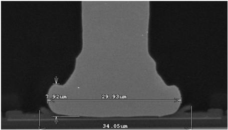
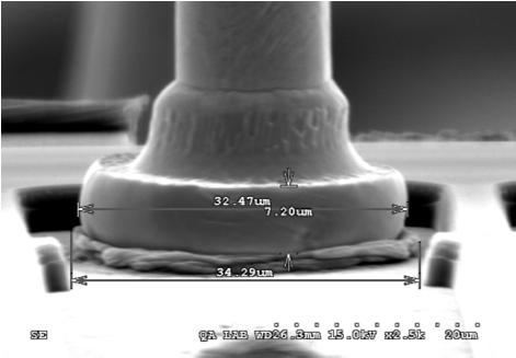
20 Resolving Pad Crack For Cu Wire Bonding Process Ball Dia (um) Contact Dia (um) Splash X (um) Splash Y (um) Ball IMC% Height Avg Max Avg Max (um) Avg Min Pad Crack % Traditional Process on ProCu BSA=85 Traditional Process on ProCu Plus BSA=85 ProCu5 on ProCu Plus BSA 85 ProCu5 on ProCu Plus BSA % 90% 27% % 91% 9% % 89% % 90% 0 Traditional Process on ProCu Traditional Process On ProCu Plus ProCu5 on ProCu Plus 20


21 Improving Al Splash and IMC Y Splash (µm) Process Comparison Difference in splash ProBond ProCu4 - Better ProCu5 - Best % 65% 70% 75% 80% 85% 90% 95% 100% IMC% IMC Probond ProCu4 ProCu5 ProBond on ProCu ProCu4 on ProCu ProCu5 on ProCu Plus 21
22 Fine Pitch Advances 40um Pitch Process 15um wire/40um pitch process is tested as part of our latest equipment verification test. Portable results are achieved across all machines meeting all wire bonding specifications. We are fully capable to support 28nm and 20nm wire bonding in high volume production. Shear/ Area Ball Dia (um) Ball Height (um) Splash (µm) IMC (%) Dage Pull (gr) MC # Lift X Avg X Max Y Avg Y Max XY Avg Avg Min Avg Min (gr/mil 2 ) Peel Spec >7 27 ± ± 1.5 <34um <34um >85% >80% >2.5 0% MC % 88% % MC % 86% % MC % 84% % MC % 90% % MC % 86% % Avg % 87% Min % 84% Max % 90%
23 Reliability Study of Fine Pitch Cu Process Cell Wire Dia. [um] Ball Dia. [um] Y- Splash. [um] Shear [g] Cont. Dia. [um] IMC [%] Al remain [%] HAST 96hr Failure HAST 168hr Failure HAST 96hr Failure HAST 336hr Failure % 16% 0% 0% % 9% 0% 0% % 0% 0% 0% % 0% 0% 0% % 0% 0% 0% % 0% Did not test Smaller bonded ball diameter negatively affects reliability outcome. Med Grade EMC Low Cl, Low Cl + Ion Trapper EMCs Better molding compounds with low Cl and Ion Trapper can easily pass 336 hour bias HAST reliability test for all cells. 30um bonded ball is targeted for 40um pitch application. This shows that reliable 40 um pitch Cu wire bond process is achievable. 23


24 28nm ELK Wafer Status Major foundries wafer qualified Multiple customer s device qualification pass Multiple customer s device already production MP Avg. yield performance 99.88% since May 1 st bond X-section Source: ASE 24

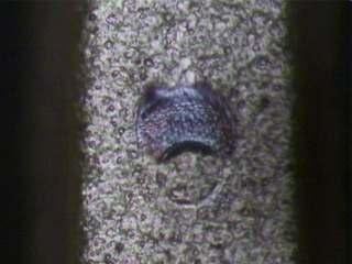
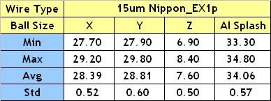
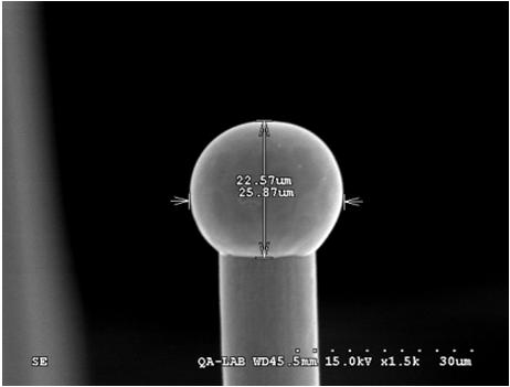
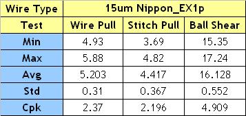


25 15um Cu Wire Development 28nm ELK, 35um Bond Pad Opening After ball shear After stitch pull Source ASE 25


26 20nm ELK Wafer Development Device information Package type : PBGA Package size: 31 x 31mm Lead count: 899L Die size : 7.9 x 7.9mm Bond pad pitch: 45um Bond pad opening: 40um Al layer thickness: 1.4um Pad structure : DS W/B control Machine : K&S ProCu Bonder Wire diameter: 18um Cu coating wire Status Under Reliability test Source: ASE 26
 Ball Height (um) Shear (g) X Splash (µm) Y Splash")
 Average 24.1 6.1 6.9 27.8 28.7 96% 19.9 3.8 2.7 Stdev 0.")


27 Cu Wire Fine Pitch Capability 13µm wire / 35um Pitch Ball Dia (um) Ball Height (um) Shear (g) X Splash (µm) Y Splash (µm) IMC (%) Contact Dia (µm) 1st bond Pull (g) 2nd Bond Pull (g) Average % Stdev % Max % Min % Range % Achieved Good Free Air Ball, 1 st bond, 2 nd bond and Looping performance 27
 Shear Avg (g) X Splash Avg (um) Y Splash Avg (um) Y Splash Max")
 65 24.3 6.2 6.3 27.8 27.7 29.")

28 Cu Wire Fine Pitch Process Window BSA (USG) Ball Dia (um) Ball Height (um) Shear Avg (g) X Splash Avg (um) Y Splash Avg (um) Y Splash Max (um) IMC Avg (%) IMC Min (%) Contact Dia (um) Pull Avg (g) BSA = 65 BSA = 70 BSA = 75 Pull Min (g) % 89% % 0% % 91% % 0% % 96% % 0% Lift Peels 28

29 Copper Wire Bond Looping Challenges PdCu wire is stronger than Au, it has better looping capability for fine pitch, multi-tier devices The Challenge is Complexity! Applications have increasing wire counts We provided new loop profiles & with advanced trajectory control to achieve good results Many wires with many loop profiles is a teaching and optimization challenge We are working to make this task easier Advanced node Application: > 500 wires mil PdCu wire Up to 8 layers of loops wire length up to 200 mils loop heights up to 400um 29


30 K&S AutoOLP AutoOLP is a system which convert device drawings into wire bonding program (recipes) in minimal time. We are adding new capability of 3D loop clearance check. Setup CAD Drawing Set Loop Parameters 3D Display & Clearance Checking Satisfied Program Generation Bonder Not Satisfied One By One Group Load Bonder Recipe back to AutoOLP in 3D View 30
31 QFN (Quad-Flat pack No-Lead)- the fastest growing wire bond package Source : Prismark 31 31


32 QFN Device Samples 32


33 QFN Overview The benefits of QFN include low cost, reduced lead inductance, a small "near chip scale" footprint, thin profile and low weight. First bond processes are generally not an issue on QFNs Second bond can be difficult for several reasons Effective leadfinger clamping is impossible for most QFN designs Silicone adhesive backing tape provides no anchoring of leadfingers QFN Lead-beams are highly prone to resonate under ultrasonic energy New plating types (PPF, µppf) and roughened surfaces are less bondable compared to traditional Ag plating 33


34 Advances in QFN 2 nd Bond ProStitch Plus Process Uses response based parameters Provide similarity in the look & feel of interface to ProCu. Stitch parameters initialized for processes based on material set information wire diameter, cap geometry, etc. Fine adjustment parameters will optimize the process to account for difference in applications. 34


35 Process Improvement Example 0.8mil Bare Cu and AuPdCu Wire on PPF QFN ProStitch process Maxsoft Bare Cu: 100% NSOL. EX1p AuPdCu: 0% Cu remain and low stitch strength. ProStitch Plus process Bare Cu and AuPdCu wire both have good results. Process type Traditional Process ProStitch Plus Wire type Maxsoft EX1p Maxsoft EX1p NSOL/SHTL 100%NSOL OK OK OK Peel OK OK OK Cu remain Most 0% 100% 100% Stitch strength avg Stitch strength min Stitch strength std Cpk(lsl=2.5)
36 Conclusion Wire bonding has improved significantly over its technology life Advanced in Cu wire bonding pushed envelope for bonding advanced packages and also enables the packaging to be cheaper K&S will continue improving our wire bonding technology As well as working on other advanced packaging technology to support the future interconnect requirement 36
37 This PowerPoint presentation and all of its contents are protected under International and United States Copyright laws. Any reproduction or use of all or any part of this presentation without the express written consent of K&S is prohibited. 37
Interconnection Challenge in Wire Bonding Ag alloy wire. Jensen Tsai / 蔡瀛洲, SPIL, Taiwan
 1 Interconnection Challenge in Wire Bonding Ag alloy wire Jensen Tsai / 蔡瀛洲, SPIL, Taiwan 2 Content Ag Alloy Wire Type Market Ag Alloy Wire Benefits Workability and Reliability Performance IMC behavior
Wirebond challenges in QFN. Engineering Team - Wire bond section SPEL Semiconductor Limited
 Introduction: Wirebond challenges in QFN by Engineering Team - Wire bond section SPEL Semiconductor Limited The market for the portable & handheld consumer electronic goods is growing rapidly and technological
The Future of Packaging ~ Advanced System Integration
 The Future of Packaging ~ Advanced System Integration Enabling a Microelectronic World R. Huemoeller SVP, Adv. Product / Platform Develop June 2013 Product Segments End Market % Share Summary 2 New Product
سمینار درس تئوری و تکنولوژی ساخت
 نام خدا به 1 سمینار درس تئوری و تکنولوژی ساخت Wire Bonding استاد : جناب آقای محمدنژاد دکتر اردیبهشت 93 2 3 Content IC interconnection technologies Whats wirebonding Wire Bonding Processes Thermosonic Wirebond
EFFECTS OF USG CURRENT AND BONDING LOAD ON BONDING FORMATION IN QFN STACKED DIE PACKAGE. A. Jalar, S.A. Radzi and M.A.A. Hamid
 Solid State Science and Technology, Vol. 16, No 2 (2008) 65-71 EFFECTS OF USG CURRENT AND BONDING LOAD ON BONDING FORMATION IN QFN STACKED DIE PACKAGE A. Jalar, S.A. Radzi and M.A.A. Hamid School of Applied
POSSUM TM Die Design as a Low Cost 3D Packaging Alternative
 POSSUM TM Die Design as a Low Cost 3D Packaging Alternative The trend toward 3D system integration in a small form factor has accelerated even more with the introduction of smartphones and tablets. Integration
Comparative Analyses between Bare Cu Wire and Palladium Coated Cu Wire Performance in IC Packaging Assembly
 Comparative Analyses between Bare Cu Wire and Palladium Coated Cu Wire Performance in IC Packaging Assembly Dr. Jerome Palaganas NANOTECH Solutions, Inc. jerome@satech8.com ABSTRACT Cu wirebonding has
MEPTEC Luncheon Presentation. Introduction of Ag Alloy Bonding Wire William (Bud) Crockett Jr.
 Crockett Jr.") MEPTEC Luncheon Presentation Introduction of Ag Alloy Bonding Wire William (Bud) Crockett Jr. w-crockett@ml.tanaka.co.jp April 10, 2013 2012 Semiconductor Market Tracking Forbes 2012 Monthly rolling forecast
MEPTEC Luncheon Presentation Introduction of Ag Alloy Bonding Wire William (Bud) Crockett Jr. w-crockett@ml.tanaka.co.jp April 10, 2013 2012 Semiconductor Market Tracking Forbes 2012 Monthly rolling forecast
ENGINEERING PRACTICE STUDY FINAL REPORT STUDY PROJECT September 20, 2017
 ENGINEERING PRACTICE STUDY TITLE: Copper (Cu) wire bond test methodology development for microcircuit, hybrid and semiconductor devices FINAL REPORT STUDY PROJECT 5962-2017-002 September 20, 2017 Study
B. Flip-Chip Technology
 B. Flip-Chip Technology B1. Level 1. Introduction to Flip-Chip techniques B1.1 Why flip-chip? In the development of packaging of electronics the aim is to lower cost, increase the packaging density, improve
SESUB - Its Leadership In Embedded Die Packaging Technology
 SESUB - Its Leadership In Embedded Die Packaging Technology Sip Conference China 2018 TDK Corporation ECBC, PAF, SESUB BU Kofu, Japan October 17, 2018 Contents SESUB Introduction SESUB Process SESUB Quality
Brief Introduction of Sigurd IC package Assembly
 Brief Introduction of Sigurd IC package Assembly Content Package Development Trend Product Brief Sawing type QFN Representative MEMS Product LGA Light Sensor Proximity Sensor High Yield Capability Low
Stack Die CSP Interconnect Challenges Flynn Carson, Glenn Narvaez, HC Choi, and DW Son ChipPAC, Inc.
 Stack Die CSP Interconnect Challenges Flynn Carson, Glenn Narvaez, HC Choi, and DW Son ChipPAC, Inc. IEEE/CPMT Seminar Overview 4 Stacked die Chip Scale Packages (CSPs) enable more device functionality
Packaging Roadmap: The impact of miniaturization. Bob Pfahl, inemi Celestica-iNEMI Technology Forum May 15, 2007
 Packaging Roadmap: The impact of miniaturization Bob Pfahl, inemi Celestica-iNEMI Technology Forum May 15, 2007 The Challenges for the Next Decade Addressing the consumer experience using the converged
Challenges of Ultimate Ultra-Fine Pitch Process with Gold Wire & Copper Wire in QFN Packages
 Challenges of Ultimate Ultra-Fine Pitch Process with Gold Wire & Copper Wire in QFN Packages C.E.Tan, J.Y.Liong, Jeramie Dimatira, Jason Tan* & Lee Wee Kok** ON Semiconductor Lot 122, Senawang Industrial
MICROELECTRONICS ASSSEMBLY TECHNOLOGIES. The QFN Platform as a Chip Packaging Foundation
 West Coast Luncheon January 15, 2014. PROMEX PROMEX INDUSTRIES INC. MICROELECTRONICS ASSSEMBLY TECHNOLOGIES The QFN Platform as a Chip Packaging Foundation 3075 Oakmead Village Drive Santa Clara CA Ɩ 95051
Compression Molding. Solutions for 3D TSV and other advanced packages as well as cost savings for standard package applications
 Compression Molding Solutions for 3D TSV and other advanced packages as well as cost savings for standard package applications 1. Company Introduction 2. Package Development Trend 3. Compression FFT Molding
23. Packaging of Electronic Equipments (2)
") 23. Packaging of Electronic Equipments (2) 23.1 Packaging and Interconnection Techniques Introduction Electronic packaging, which for many years was only an afterthought in the design and manufacture of
23. Packaging of Electronic Equipments (2) 23.1 Packaging and Interconnection Techniques Introduction Electronic packaging, which for many years was only an afterthought in the design and manufacture of
Innovations Push Package-on-Package Into New Markets. Flynn Carson. STATS ChipPAC Inc Kato Rd Fremont, CA 94538
 Innovations Push Package-on-Package Into New Markets by Flynn Carson STATS ChipPAC Inc. 47400 Kato Rd Fremont, CA 94538 Copyright 2010. Reprinted from Semiconductor International, April 2010. By choosing
Abstract. Key words: Interconnections, wire bonding, Ball Grid Arrays, metallization
 Integrated Solutions to Bonding BGA Packages: Capillary, Wire, and Machine Considerations by Leroy Christie, Director Front Line Process Engineering AMKOR Electronics 1900 South Price Road, Chandler, Az
Hermetic Packaging Solutions using Borosilicate Glass Thin Films. Lithoglas Hermetic Packaging Solutions using Borosilicate Glass Thin Films
 Hermetic Packaging Solutions using Borosilicate Glass Thin Films 1 Company Profile Company founded in 2006 ISO 9001:2008 qualified since 2011 Headquarters and Production in Dresden, Germany Production
Tips for Increasing Yields when Wire Bonding Small MESA Chips TECH BRIEF
 Tips for Increasing Yields when Wire Bonding Small MESA Chips TECH BRIEF Abstract: lorem ipsum dolor sit amet Small MESA devices have posed a number of wire-bonding challenges, which have required advancements
Wire Bond Technology The Great Debate: Ball vs. Wedge
 Wire Bond Technology The Great Debate: Ball vs. Wedge Donald J. Beck, Applications Manager Alberto C. Perez, Hardware and Applications Engineer Palomar Technologies, Inc. 2728 Loker Avenue West Carlsbad,
Stitch Bond Enhancement for X-Wire Insulated Bonding Wire
 Stitch Bond Enhancement for X-Wire Insulated Bonding Wire A Technical Collaboration Published by: Small Precision Tools www.smallprecisiontools.com and Microbonds Inc. www.microbonds.com 2007 Microbonds
Introduction to Wire-Bonding
 Introduction to Wire-Bonding Wire bonding is a kind of friction welding Material are connected via friction welding Advantage: Different materials can be connected to each other widely used, e.g. in automobile
3D TSV Micro Cu Column Chip-to-Substrate/Chip Assmbly/Packaging Technology
 3D TSV Micro Cu Column Chip-to-Substrate/Chip Assmbly/Packaging Technology by Seung Wook Yoon, *K. T. Kang, W. K. Choi, * H. T. Lee, Andy C. B. Yong and Pandi C. Marimuthu STATS ChipPAC LTD, 5 Yishun Street
MIL-STD-883E METHOD BOND STRENGTH (DESTRUCTIVE BOND PULL TEST)
") BOND STRENGTH (DESTRUCTIVE BOND PULL TEST) 1. PURPOSE. The purpose of this test is to measure bond strengths, evaluate bond strength distributions, or determine compliance with specified bond strength
BOND STRENGTH (DESTRUCTIVE BOND PULL TEST) 1. PURPOSE. The purpose of this test is to measure bond strengths, evaluate bond strength distributions, or determine compliance with specified bond strength
450mm and Moore s Law Advanced Packaging Challenges and the Impact of 3D
 450mm and Moore s Law Advanced Packaging Challenges and the Impact of 3D Doug Anberg VP, Technical Marketing Ultratech SOKUDO Lithography Breakfast Forum July 10, 2013 Agenda Next Generation Technology
Silicon Interposers enable high performance capacitors
 Interposers between ICs and package substrates that contain thin film capacitors have been used previously in order to improve circuit performance. However, with the interconnect inductance due to wire
Enabling concepts: Packaging Technologies
 Enabling concepts: Packaging Technologies Ana Collado / Liam Murphy ESA / TEC-EDC 01/10/2018 ESA UNCLASSIFIED - For Official Use Enabling concepts: Packaging Technologies Drivers for the future: Higher
SWTW 2000, June Assessing Pad Damage and Bond Integrity for Fine Pitch Probing
 SWTW 2000, June 11-14 Assessing Pad Damage and Bond Integrity for Fine Pitch Probing Dean Gahagan, Pyramid Probe Division, Cascade Microtech & Lee Levine, Kulicke & Soffa Industries Challenges of die shrinks
2.5D Platform (Examples of products produced to date are shown here to demonstrate Amkor's production capabilities)
") Wafer Finishing & Flip Chip Stacking interconnects have emerged to serve a wide range of 2.5D- & 3D- packaging applications and architectures that demand very high performance and functionality at the
Wafer Finishing & Flip Chip Stacking interconnects have emerged to serve a wide range of 2.5D- & 3D- packaging applications and architectures that demand very high performance and functionality at the
SiP packaging technology of intelligent sensor module. Tony li
 SiP packaging technology of intelligent sensor module Tony li 2016.9 Contents What we can do with sensors Sensor market trend Challenges of sensor packaging SiP technology to overcome challenges Overview
Chapter 2. Literature Review
 Chapter 2 Literature Review 2.1 Development of Electronic Packaging Electronic Packaging is to assemble an integrated circuit device with specific function and to connect with other electronic devices.
Flip-Chip for MM-Wave and Broadband Packaging
 1 Flip-Chip for MM-Wave and Broadband Packaging Wolfgang Heinrich Ferdinand-Braun-Institut für Höchstfrequenztechnik (FBH) Berlin / Germany with contributions by F. J. Schmückle Motivation Growing markets
Chapter 7 Introduction to 3D Integration Technology using TSV
 Chapter 7 Introduction to 3D Integration Technology using TSV Jin-Fu Li Department of Electrical Engineering National Central University Jungli, Taiwan Outline Why 3D Integration An Exemplary TSV Process
Advances in stacked-die packaging
 pg.10-15-carson-art 16/6/03 4:12 pm Page 1 The stacking of die within IC packages, primarily Chip Scale Packages (CSP) Ball Grid Arrays (BGAs) has evolved rapidly over the last few years. The now standard
23 rd ASEMEP National Technical Symposium
 V3V3D VSS GPIO0_SA GPIO1_SA AF E_ S CLK_SA AFE_ RST_SA VSS GPI O1 _A GPI O0 _AAF E_ FR _RDYAFE_ RST AFE_SCS AFE_SCLKAFE_SDA0A F E_ S D A1 V3V3D V3V3D VSS GPI O3 MS DA MS CL GPI O2 GPI O1 GPI O0 TSDA TSCL
UMS User guide for bare dies GaAs MMIC. storage, pick & place, die attach and wire bonding
 UMS User guide for bare dies GaAs MMIC storage, pick & place, die attach and wire bonding Ref. : AN00014097-07 Apr 14 1/10 Specifications subject to change without notice United Monolithic Semiconductors
INCREASING PACKAGE ROBUSTNESS WITH PALLADIUM COATED COPPER WIRE
 INCREASING PACKAGE ROBUSTNESS WITH PALLADIUM COATED COPPER WIRE Rodan A. Melanio Regine B. Cervantes Sonny E. Dipasupil New Package Development ON Semiconductor Philippines Incorporated Golden Mile Business
Data Sheet _ R&D. Rev Date: 8/17
 Data Sheet _ R&D Rev Date: 8/17 Micro Bump In coming years the interconnect density for several applications such as micro display, imaging devices will approach the pitch 10um and below. Many research
Flexline - A Flexible Manufacturing Method for Wafer Level Packages (Extended Abstract)
") Flexline - A Flexible Manufacturing Method for Wafer Level Packages (Extended Abstract) by Tom Strothmann, *Damien Pricolo, **Seung Wook Yoon, **Yaojian Lin STATS ChipPAC Inc.1711 W Greentree Drive Tempe,
Flexline - A Flexible Manufacturing Method for Wafer Level Packages (Extended Abstract) by Tom Strothmann, *Damien Pricolo, **Seung Wook Yoon, **Yaojian Lin STATS ChipPAC Inc.1711 W Greentree Drive Tempe,
ARCHIVE Brandon Prior Senior Consultant Prismark Partners ABSTRACT
 ARCHIVE 2010 LOW COST, SMALL FORM FACTOR PACKAGING by Brandon Prior Senior Consultant Prismark Partners W ABSTRACT hile size reduction and performance improvement are often the drivers of new package and
The Role of Flip Chip Bonding in Advanced Packaging David Pedder
 The Role of Flip Chip Bonding in Advanced Packaging David Pedder David Pedder Associates Stanford in the Vale Faringdon Oxfordshire The Role of Flip Chip Bonding in Advanced Packaging Outline Flip Chip
New Approaches to Develop a Scalable 3D IC Assembly Method
 New Approaches to Develop a Scalable 3D IC Assembly Method Charles G. Woychik Ph.D. Sangil Lee, Ph.D., Scott McGrath, Eric Tosaya and Sitaram Arkalgud Ph.D. Invensas Corporation 3025 Orchard Parkway San
Abstract. Key words: Insulated bonding wire, Advanced Packaging, Wire bonding
 Robust Wirebonding of X-Wire Insulated Bonding Wire Technology Christopher Carr, Juan Munar, William Crockett, Robert Lyn Microbonds Inc. 151 Amber St. Unit 12 Markham, Ontario, Canada L3R 3B3 Tel: 905-305-0980,
Substrates Lost in Translation
 2004 IEEE PRESENTATION Components, Packaging & Manufacturing Technology (CPMT) Society, Santa Clara Valley Chapter www.cpmt.org/scv/ Substrates Lost in Translation R. Huemoeller Vice President, Substrate
Tape Automated Bonding
 Tape Automated Bonding Introduction TAB evolved from the minimod project begun at General Electric in 1965, and the term Tape Automated Bonding was coined by Gerard Dehaine of Honeywell Bull in 1971. The
General Rules for Bonding and Packaging
 General Rules for Bonding and Packaging at the Else Kooi Laboratory 3 CONTENT Rules for assembly at EKL 4 Introduction to assembly 5 Rules for Saw Lane 7 Rules for Chip Size 8 Rules for Bondpads 9 Rules
Image Sensor Advanced Package Solution. Prepared by : JL Huang & KingPak RD division
 Image Sensor Advanced Package Solution Prepared by : JL Huang & KingPak RD division Contents CMOS image sensor marketing overview Comparison between different type of CMOS image sensor package Overview
Impact of Young Modulus of Epoxy Glue to Copper Wire Bonding
 Impact of Young Modulus of Epoxy Glue to Copper Wire Bonding Tan KG 1, Chung EL 1, Wai CM 1, Ge Dandong 2 1 Infineon Technologies (Malaysia) Sdn Bhd, Malaysia 2 Infineon Technologies Asia Pacific Pte Ltd,
TAIPRO Engineering. Speaker: M. Saint-Mard Managing director. TAIlored microsystem improving your PROduct
 TAIPRO Engineering MEMS packaging is crucial for system performance and reliability Speaker: M. Saint-Mard Managing director TAIPRO ENGINEERING SA Michel Saint-Mard Administrateur délégué m.saintmard@taipro.be
Min Tao, Ph. D, Ashok Prabhu, Akash Agrawal, Ilyas Mohammed, Ph. D, Bel Haba, Ph. D Oct , IWLPC
 PACKAGE-ON-PACKAGE INTERCONNECT FOR FAN-OUT WAFER LEVEL PACKAGES Min Tao, Ph. D, Ashok Prabhu, Akash Agrawal, Ilyas Mohammed, Ph. D, Bel Haba, Ph. D Oct 18-20 2016, IWLPC 1 Outline Laminate to Fan-Out
Challenges and More Challenges SW Test Workshop June 9, 2004
 Innovating Test Technologies Challenges and More Challenges SW Test Workshop June 9, 2004 Cascade Microtech Pyramid Probe Division Ken Smith Dean Gahagan Challenges and More Challenges Probe card requirements
Specifications subject to change Packaging
 VCSEL Standard Product Packaging Options All standard products are represented in the table below. The Part Number for a standard product is determined by replacing the x in the column Generic Part Number
Two major features of this text
 Two major features of this text Since explanatory materials are systematically made based on subject examination questions, preparation
High Efficient Heat Dissipation on Printed Circuit Boards. Markus Wille, R&D Manager, Schoeller Electronics Systems GmbH
 High Efficient Heat Dissipation on Printed Circuit Boards Markus Wille, R&D Manager, Schoeller Electronics Systems GmbH m.wille@se-pcb.de Introduction 2 Heat Flux: Q x y Q z The substrate (insulation)
10nm CPI Study for Fine Pitch Flip Chip Attach Process and Substrate
 10nm CPI Study for Fine Pitch Flip Chip Attach Process and Substrate Ming-Che Hsieh, Chi-Yuan Chen*, Ian Hsu*, Stanley Lin* and KeonTaek Kang** Product and Technology Marketing / STATS ChipPAC Pte. Ltd.
Fabricating 2.5D, 3D, 5.5D Devices
 Fabricating 2.5D, 3D, 5.5D Devices Bob Patti, CTO rpatti@tezzaron.com Tezzar on Semiconduct or 04/15/2013 1 Gen4 Dis-Integrated 3D Memory DRAM layers 42nm node 2 million vertical connections per lay per
Fraunhofer IZM - ASSID
 FRAUNHOFER-INSTITUT FÜR Zuverlässigkeit und Mikrointegration IZM Fraunhofer IZM - ASSID All Silicon System Integration Dresden Heterogeneous 3D Wafer Level System Integration 3D system integration is one
An Introduction to Electronics Systems Packaging. Prof. G. V. Mahesh. Department of Electronic Systems Engineering
 An Introduction to Electronics Systems Packaging Prof. G. V. Mahesh Department of Electronic Systems Engineering India Institute of Science, Bangalore Module No. # 02 Lecture No. # 08 Wafer Packaging Packaging
Process Certification and Defect Recognition: Hybrids, Microcircuits and RF/MMIC Modules (3 DAYS)
") Process Certification and Defect Recognition: Hybrids, Microcircuits and RF/MMIC Modules (3 DAYS) Course Description: Most companies struggle to introduce new lines and waste countless manhours and resources
Process Certification and Defect Recognition: Hybrids, Microcircuits and RF/MMIC Modules (3 DAYS) Course Description: Most companies struggle to introduce new lines and waste countless manhours and resources
3D ICs: Recent Advances in the Industry
 3D ICs: Recent Advances in the Industry Suresh Ramalingam Senior Director, Advanced Packaging Outline 3D IC Background 3D IC Technology Development Summary Acknowledgements Stacked Silicon Interconnect
TSV MEOL (Mid-End-Of-Line) and its Assembly/Packaging Technology for 3D/2.5D Solutions
 and its Assembly/Packaging Technology for 3D/2.5D Solutions") TSV MEOL (Mid-End-Of-Line) and its Assembly/Packaging Technology for 3D/2.5D Solutions Seung Wook YOON, D.J. Na, *K. T. Kang, W. K. Choi, C.B. Yong, *Y.C. Kim and Pandi C. Marimuthu STATS ChipPAC Ltd.
TSV MEOL (Mid-End-Of-Line) and its Assembly/Packaging Technology for 3D/2.5D Solutions Seung Wook YOON, D.J. Na, *K. T. Kang, W. K. Choi, C.B. Yong, *Y.C. Kim and Pandi C. Marimuthu STATS ChipPAC Ltd.
Two capillary solutions for ultra-fine-pitch wire bonding and insulated wire bonding
 Microelectronic Engineering 84 (2007) 362 367 www.elsevier.com/locate/mee Two capillary solutions for ultra-fine-pitch wire bonding and insulated wire bonding K.S. Goh a, Z.W. Zhong b, * a SPT Asia Pte
Intel's 65 nm Logic Technology Demonstrated on 0.57 µm 2 SRAM Cells
 Intel's 65 nm Logic Technology Demonstrated on 0.57 µm 2 SRAM Cells Mark Bohr Intel Senior Fellow Director of Process Architecture & Integration Intel 1 What are We Announcing? Intel has fabricated fully-functional
Chapter 11 Testing, Assembly, and Packaging
 Chapter 11 Testing, Assembly, and Packaging Professor Paul K. Chu Testing The finished wafer is put on a holder and aligned for testing under a microscope Each chip on the wafer is inspected by a multiple-point
Challenges of Ultra-thin LGA Package for Fingerprint Sensors
 Challenges of Ultra-thin LGA Package for Fingerprint Sensors Jensen Tsai Deputy Director, SPIL Outline Background Package Features & Challenges Challenges & Solutions Mold Clearance Low Wire Loop Height
Market and technology trends in advanced packaging
 Close Market and technology trends in advanced packaging Executive OVERVIEW Recent advances in device miniaturization trends have placed stringent requirements for all aspects of product manufacturing.
22 nd ASEMEP National Technical Symposium
 QUAD FLAT NO-LEAD (QFN) FINE PITCH PACKAGING DESIGN AND MANUFACTURING CHALLENGES Michael B. Tabiera Ricky B. Calustre Jefferson S. Talledo Corporate Packaging & Automation STMicroelectronics, Inc., Calamba
Laminate Based Fan-Out Embedded Die Technologies: The Other Option
 Laminate Based Fan-Out Embedded Die Technologies: The Other Option Theodore (Ted) G. Tessier, Tanja Karila*, Tuomas Waris*, Mark Dhaenens and David Clark FlipChip International, LLC 3701 E University Drive
Product Catalog. Semiconductor Intellectual Property & Technology Licensing Program
 Product Catalog Semiconductor Intellectual Property & Technology Licensing Program MANUFACTURING PROCESS TECHNOLOGY OVERVIEW 90 nm 130 nm 0.18 µm 0.25 µm 0.35 µm >0.40 µm Logic CMOS SOI CMOS SOI CMOS SOI
High Reliability and High Temperature Application Solution Solder Joint Encapsulant Paste
 High Reliability and High Temperature Application Solution Solder Joint Encapsulant Paste YINCAE Advanced Materials, LLC WHITE PAPER October 2017 2017 YINCAE Advanced Materials, LLC - All Rights Reserved.
QUALIFICATION PLAN PCN #: IIRA-05BPMD768. Date: Dec 18, Qualification of 132L DQFN package at ANAC assembly site. A.
 QUALIFICATION PLAN PCN #: IIRA-05BPMD768 Date: Dec 18, 2013 Qualification of 132L DQFN package at ANAC assembly site. Distribution Surasit P. Rangsun K A. Navarro Irina K Wichai K. Fernando C Chaweng W.
SOLDERABLE ANISOTROPIC CONDUCTIVE ADHESIVES FOR 3D PACKAGE APPLICATIONS
 SOLDERABLE ANISOTROPIC CONDUCTIVE ADHESIVES FOR 3D PACKAGE APPLICATIONS ABSTRACT: Dr. Mary Liu and Dr. Wusheng Yin YINCAE Advanced Materials, LLC Albany, NY 3D packaging has recently become very attractive
Pull Force and Tail Breaking Force Optimization of the Crescent Bonding Process with Insulated Au Wire. Experimental
 Pull Force and Tail Breaking Force Optimization of the Crescent Bonding Process with Insulated Au 1 J. Lee, 1 M. Mayer, 1 Y. Zhou and 2 J. Persic 1 Microjoining Lab, Centre of Advanced Materials Joining,
ACOUSTIC MICRO IMAGING ANALYSIS METHODS FOR 3D PACKAGES
 ACOUSTIC MICRO IMAGING ANALYSIS METHODS FOR 3D PACKAGES Janet E. Semmens Sonoscan, Inc. Elk Grove Village, IL, USA Jsemmens@sonoscan.com ABSTRACT Earlier studies concerning evaluation of stacked die packages
Through-Silicon-Via Inductor: Is it Real or Just A Fantasy?
 Through-Silicon-Via Inductor: Is it Real or Just A Fantasy? Umamaheswara Rao Tida 1 Cheng Zhuo 2 Yiyu Shi 1 1 ECE Department, Missouri University of Science and Technology 2 Intel Research, Hillsboro Outline
Design and Development of True-CSP
 Design and Development of True-CSP *Kolan Ravi Kanth, Francis K.S. Poh, B.K. Lim, Desmond Y.R. Chong, Anthony Sun, H.B. Tan United Test & Assembly Center Ltd (UTAC) 5 Serangoon North Ave 5, Singapore 554916
West Bond Model 7476E-79 Wedge Wire Bonder STANDAR OPERATING PROCEDURE Version: 1.0 March 2014
 West Bond Model 7476E-79 Wedge Wire Bonder STANDAR OPERATING PROCEDURE Version: 1.0 March 2014 UNIVERSITY OF TEXAS AT ARLINGTON Nanotechnology Research Center (NRC) TABLE OF CONTENTS 1. Introduction....3
77 GHz VCO for Car Radar Systems T625_VCO2_W Preliminary Data Sheet
 77 GHz VCO for Car Radar Systems Preliminary Data Sheet Operating Frequency: 76-77 GHz Tuning Range > 1 GHz Output matched to 50 Ω Application in Car Radar Systems ESD: Electrostatic discharge sensitive
TSI, or through-silicon insulation, is the
 Vertical through-wafer insulation: Enabling integration and innovation PETER HIMES, Silex Microsystems AB, Järfälla SWEDEN Through-wafer insulation has been used to develop technologies such as Sil-Via
1. Exceeding these limits may cause permanent damage.
 Silicon PIN Diode s Features Switch & Attenuator Die Extensive Selection of I-Region Lengths Hermetic Glass Passivated CERMACHIP Oxide Passivated Planar s Voltage Ratings to 3000V Faster Switching Speed
IMAGE SENSOR EVOLUTION AND ENABLING 3D TECHNOLOGIES
 Fig. 5: Scanning Electron Microscopy images (TOP view, 3D view, Zoome including all metal levels of the BSI imager structure. (dashed line shows bonding IMAGE SENSOR EVOLUTION AND ENABLING 3D TECHNOLOGIES
IMAPS NE 45 A HETEROGENEOUS SIP SOLUTION FOR RF APPLICATIONS
 IMAPS NE 45 A HETEROGENEOUS SIP SOLUTION FOR RF APPLICATIONS May 1st 2018 Justin C. Borski i3 Microsystems Inc. justin.borski@i3microsystems.com A HETEROGENEOUS SIP SOLUTION FOR RF APPLICATIONS Presentation
CHAPTER 11: Testing, Assembly, and Packaging
 Chapter 11 1 CHAPTER 11: Testing, Assembly, and Packaging The previous chapters focus on the fabrication of devices in silicon or the frontend technology. Hundreds of chips can be built on a single wafer,
New Wave SiP solution for Power
 New Wave SiP solution for Power Vincent Lin Corporate R&D ASE Group APEC March 7 th, 2018 in San Antonio, Texas. 0 Outline Challenges Facing Human Society Energy, Environment and Traffic Autonomous Driving
Electroless Bumping for 300mm Wafers
 Electroless Bumping for 300mm Wafers T. Oppert Internepcon 2006 Tokyo Big Sight, Japan Outline Short Company Profile Electroless Ni/Au Under Bump Metallization UBM for Copper Devices Solder Bumping: Stencil
BCD Smart Power Roadmap Trends and Challenges. Giuseppe Croce NEREID WORKSHOP Smart Energy Bertinoro, October 20 th
 BCD Smart Power Roadmap Trends and Challenges Giuseppe Croce NEREID WORKSHOP Smart Energy Bertinoro, October 20 th Outline 2 Introduction Major Trends in Smart Power ASICs An insight on (some) differentiating
Introduction of IMS Technology for Advanced Solder Bumping on Wafers / Laminates
 Introduction of IMS Technology for Advanced Solder Bumping on Wafers / Laminates Science & Technology IBM Research Tokyo Yasumitsu Orii, PhD Senju Metal Industry Co.,TW Deputy General Manager Lewis Huang
FLIP CHIP LED SOLDER ASSEMBLY
 As originally published in the SMTA Proceedings FLIP CHIP LED SOLDER ASSEMBLY Gyan Dutt, Srinath Himanshu, Nicholas Herrick, Amit Patel and Ranjit Pandher, Ph.D. Alpha Assembly Solutions South Plainfield,
Okamoto Machine Tool Works, LTD. June 22, th SEMATECH Symposium Japan 1
 Okamoto Machine Tool Works, LTD 1 Contents Solutions for TSV Wafer Thinning Process (Front Side Via) TSV Wafer Thinning Challenges Process Improvement (4-years Development) TSV Wafer Thinning Tool (TSV300)
TechSearch International, Inc. Corporate Overview E. Jan Vardaman, President
 TechSearch International, Inc. Corporate Overview E. Jan Vardaman, President Corporate Background Founded in 1987 and headquartered in Austin, Texas Recognized around the world as a leading consulting
EMT 251 Introduction to IC Design
 EMT 251 Introduction to IC Design (Pengantar Rekabentuk Litar Terkamir) Semester II 2011/2012 Introduction to IC design and Transistor Fundamental Some Keywords! Very-large-scale-integration (VLSI) is
!"#$"%&' ()#*+,-+.&/0(
#*+,-+.&/0(") !"#$"%&' ()#*+,-+.&/0( Multi Chip Modules (MCM) or Multi chip packaging Industry s first MCM from IBM. Generally MCMs are horizontal or two-dimensional modules. Defined as a single unit containing two
!"#$"%&' ()#*+,-+.&/0( Multi Chip Modules (MCM) or Multi chip packaging Industry s first MCM from IBM. Generally MCMs are horizontal or two-dimensional modules. Defined as a single unit containing two
MMIC/RFIC Packaging Challenges Webcast (July 28, AM PST 12PM EST)
") MMIC/RFIC Packaging Challenges Webcast ( 9AM PST 12PM EST) Board Package Chip HEESOO LEE Agilent EEsof 3DEM Technical Lead 1 Agenda 1. MMIC/RFIC packaging challenges 2. Design techniques and solutions
MMIC/RFIC Packaging Challenges Webcast ( 9AM PST 12PM EST) Board Package Chip HEESOO LEE Agilent EEsof 3DEM Technical Lead 1 Agenda 1. MMIC/RFIC packaging challenges 2. Design techniques and solutions
The 3D Silicon Leader
 The 3D Silicon Leader 3D Silicon IPD for smaller and more reliable Implantable Medical Devices ATW on Advanced Packaging for Wireless Medical Devices Mohamed Mehdi Jatlaoui, Sébastien Leruez, Olivier Gaborieau,
Application Bulletin 240
 Application Bulletin 240 Design Consideration CUSTOM CAPABILITIES Standard PC board fabrication flexibility allows for various component orientations, mounting features, and interconnect schemes. The starting
End-of-line Standard Substrates For the Characterization of organic
 FRAUNHOFER INSTITUTe FoR Photonic Microsystems IPMS End-of-line Standard Substrates For the Characterization of organic semiconductor Materials Over the last few years, organic electronics have become
Odd-Form Factor Package Wire Bond Case Studies
 Odd-Form Factor Package Wire Bond Case Studies Daniel D. Evans Palomar Technologies, Inc. 2728 Loker Avenue West Carlsbad, CA 92010 Phone: (800) 854-3467 E-mail: info@bonders.com Abstract Although there