Reality Check: Challenges of mixed-signal VLSI design for high-speed optical communications
|
|
|
- Dwain Gordon
- 5 years ago
- Views:
Transcription


1 Reality Check: Challenges of mixed-signal VLSI design for high-speed optical communications


2 Mixed-signal VLSI for 100G and beyond 100G optical transport system Why single-chip CMOS? So what is so difficult? CHAIS ADC On-chip noise coupling Package and PCB design Testing issues Future challenges ECOC2009 Towards the Shannon limit Fujitsu Microelectronics Europe - 2
3 100G Optical Transport system 100G MUX To system (Router) 100G client module for * 100G Ethernet or * OTU-4 or 10 * 10G client module SFI-S / MLD / XFI SFI-S / MLD / XFI OTU-4 Framer / FEC SFI-S SFI-S 10 * 11.1 Gbps SFI-S SFI-S Precoding DSP 10 to 4 MUX ADC ADC ADC ADC 4 * 28 Gbps Electrical -> Optical Optical -> Electrical To network OTU Gbps 100G Coherent Receiver ADCDSP Optical Module ECOC2009 Towards the Shannon limit Fujitsu Microelectronics Europe - 3
4 Why single-chip CMOS for 100G? Massive data bandwidth between ADC/DAC and digital 4-channel 8b 56Gs/s ADC/DAC means 1.8Tb/s of data at interface Getting this from one chip to another costs power and chip area 10G SERDES link ~250mW/channel ~10W per ADC or DAC Critical performance factor is power efficiency, not just speed Discrete ADC/DAC (e.g SiGe) dissipating ~20W each (including I/O) are difficult to use Very high total power dissipation in package (>100W for multiple channels) Skew management/calibration problem (especially over temperature/lifetime) Single-chip CMOS solution is the Holy Grail Integrate on ASIC with >50M gates or memory (size limited by power dissipation) Leverage CMOS technology advances to drive down power and cost ADC and DAC get faster and lower power at the same rate as digital -- hopefully ECOC2009 Towards the Shannon limit Fujitsu Microelectronics Europe - 4
5 ADCDSP -- so what is so difficult? ADC is the biggest circuit design problem Ultra-high speed, low noise and jitter, low power consumption all at the same time Conventional techniques cannot easily deliver required performance Digital-analogue noise coupling Sampler/clock jitter ~100fs on same chip as DSP with >100A current spikes Wide bandwidth (>20GHz) and good S11 (up to >30GHz) Sampler, package, PCB design all very challenging with high pin count FCBGA On-chip DSP design is very out-of-the-ordinary (multiple TeraOPS) Extremely power-efficient use massive parallelism, not GHz clocks (Pentium 4 ) Test Performance verification challenges limits of test equipment Need at-speed performance verification in production, not just functional testing ECOC2009 Towards the Shannon limit Fujitsu Microelectronics Europe - 5
6 The ADC problem Wideband low-noise sampler + demultiplexer + interleaved ADC array Smaller CMOS geometries higher speed worse mismatch and noise Single 56Gs/s track/hold very difficult due to extreme speed <9ps to acquire, <9ps to transfer to following interleaved T/H stages Interleaved track/hold (e.g. 4-channel 14Gs/s) also very difficult Signal/clock delays must match to <<1ps how do you measure this? Noise, mismatch and power of cascaded circuits all adds up Multiple sampling capacitors, buffers, switches, demultiplexers Layout and interconnect extremely challenging Design the circuits, then find you can t actually connect everything up Interleaved ADC back-end is not so difficult (only in comparison!) Design for best power and area efficiency rather than highest speed Interleave as many as necessary to achieve required sampling rate 8 x 175Ms/s 8b SAR ADCs fit underneath 1 solder bump 45Gs/s per sq mm ECOC2009 Towards the Shannon limit Fujitsu Microelectronics Europe - 6
7 A 56Gs/s CMOS ADC solution CHArge-mode Interleaved Sampler (CHAIS) 14GHz VCO (1 per ADC pair) DEMUX 80 x ADC Inputs 80 x 8b ADC Outputs Clocks Input 4 Phase Sampler DEMUX A DEMUX B DEMUX C DEMUX D ADCBANK A ADCBANK B ADCBANK C ADCBANK D Digital Output 1024b 437.5MHz Trim Voltages Calibration ECOC2009 Towards the Shannon limit Fujitsu Microelectronics Europe - 7

8 Dual ADC layout (4mm x 4mm test chip) Sampler PLL Sampler Demux Bias Demux SAR ADC array ADC Refs ADC logic SAR ADC array Waveform memory ECOC2009 Towards the Shannon limit Fujitsu Microelectronics Europe - 8

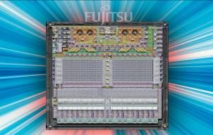
9 Example of 100G coherent receiver ASIC Architecture: Single CMOS die Technology: Interconnect: Die size: Gate count: 65nm CMOS 12 layer metal 15 mm x 15 mm ~50 million gates Package: FCBGA, >1000 pins M/S macros: 4 channel 56 Gs/s ADC 24 channel CEI-11G TX ADC power : ~2W/channel ECOC2009 Towards the Shannon limit Fujitsu Microelectronics Europe - 9
10 The DSP problem Digital design tools (and designers) *really* don t like this type of DSP The tools (and designers) synthesize circuits, then worry about how to connect them up But interconnect capacitance causes ~90% of power dissipation, not circuits Massive data bus widths (4k bits at ADC outputs) massive interconnect problem Partitioning into usable size blocks may be more difficult than it appears Tools don t like doing flat designs with tens of millions of gates (turn-around time) OK, lets split that big DSP block into two and add some pipelining Erm, about this 16k bit wide data bus you ve just introduced Better system/architecture tools for this type of design are needed Should really design/optimise the data flow, then shovel the circuits in underneath Designers brains (and system-level design tools) don t really think this way ECOC2009 Towards the Shannon limit Fujitsu Microelectronics Europe
11 On-chip noise coupling Reduce aggressor (DSP logic) noise generation Use intentional skew of clock timing within each block and between blocks Reduces peak current and spreads out in time >10x lower di/dt Lots of on-chip (~400nF) and ultra-low-inductance (~4pH) in-package decoupling Increase victim (ADC analogue) immunity Fewest possible noise/jitter sensitive circuits, all fully differential Lots of on-chip (~100nF) and low-inductance in-package decoupling Improve victim-aggressor isolation Avoid low-resistance epi substrate (short-circuit for substrate noise) Build nested walls of isolation with most sensitive circuits in the middle SAR ADCs (not jitter-sensitive) form the first line of defense Isolation walls through package and into chip form the next line Demux and other analogue circuits (calibration etc.) form the next line Sampler and PLL are hidden away inside all these layers of isolation Measurements show very little noise makes it past all the defenses ECOC2009 Towards the Shannon limit Fujitsu Microelectronics Europe
12 Package and PCB design 1mm pitch FCBGA, >1000 pins, 19 internal layers, copper lid Use similar package for test chips as typical ASIC to get same performance Low-loss high-tce LTCC (12ppm/C) for improved second-level reliability Multiple power/ground regions and shields for noise isolation Ultra-low-inductance internal decoupling for supplies and bias/reference Multiple interleaved VDD/VSS planes connect chip to multi-terminal decouplers Noise dealt with inside package predictable (stops end user getting it wrong) Coaxial via and waveguide structures, <1dB loss at 20GHz Ground planes completely removed above signal balls to reduce capacitance Dual 100ohm balanced lines used to connect coaxial via structure to G-S-G pads Optimized launch to G-S-G coplanar waveguide on low-loss PCB Balls on row inside signal pins removed to reduce capacitance, grounds cut back Outer PCB layers use MEW Megtron 6 (very low loss, lead-free multilayer compatible) ECOC2009 Towards the Shannon limit Fujitsu Microelectronics Europe


13 Package + PCB EM field simulations ECOC2009 Towards the Shannon limit Fujitsu Microelectronics Europe

14 BATBOARD and ROBIN ECOC2009 Towards the Shannon limit Fujitsu Microelectronics Europe
15 Bandwidth measurement using TDR step HP8665B Signal Generator Agilent DCA-J 86100C Picosecond Pulse Labs TDR heads <10ps risetime Model 4022 TDR/TDT Source Model 4020RPH-RP head REFCLK 1.75GHz Differential Reference Clock CH1 CH2 ADC_INP ADC_INM BATBOARD Colby Instruments delay line with 1ps resolution Model 4020RPH-RN head SPI Interface PC running MATLAB ECOC2009 Towards the Shannon limit Fujitsu Microelectronics Europe
16 Frequency Response (test setup and ADC) Frequency response of test setup TDR step (measured) Batboard PCB (measured) ENIG not Ag finish (Ni is lossy!) Socket (estimated 20 GHz) Test setup loss similar to ADC response Corrected ADC frequency response accurate measurements are not easy ADC -3dB bandwidth ~ 15GHz very close to simulation and specification ECOC2009 Towards the Shannon limit Fujitsu Microelectronics Europe
17 Production test Need proper performance verification, not just functionality Increased confidence that chip actually meets design specifications Make chip self-testing as far as possible and do at-speed performance tests Drive ADC inputs from wideband n-way power combiners Sum outputs of multiple CEI-11G channels with sinewave input(s) Enable and disable channels/clocks instead of switching (avoid 20GHz+ relays) Test ADC ENOB using sinewave input(s) Sampled data stored in on-chip RAMs then read out and analysed (ENOB) Signal source TBD (filtered DRO? phase locked to REF?) high quality essential Test CEI-11G outputs by looping back into 56Gs/s ADC inputs 5 samples per bit gives complete waveform analysis on *all* TX channels Full-speed measurement of eye opening and jitter ECOC2009 Towards the Shannon limit Fujitsu Microelectronics Europe
18 Future challenges -- what obstacles are there to progress beyond 100Gb/s? Sampler noise/bandwidth/interleave skew/clock jitter Can be solved using new CMOS techniques instead of exotic technology CHAIS sampler/demux/adc is capable of >100Gs/s even in 65nm Bandwidth scales with clock rate (-3dB at ~0.3Fs) Input bandwidth increase and S11 improvement FBGA package modifications to optimize design for very high frequencies Smaller ball pitch conflicts with second-level reliability and PCB issues Power consumption DSP issue, ADC is ~2W/channel (65nm, scales like digital) DSP power is several times ADC power, especially with more complex systems Power increase (complexity) is outrunning power savings (process shrink) Layout (interconnect and floorplan) feasibility Everything wants to be on top of everything else with zero-length connections Could need unconventional layouts ADCs might look like dartboards ECOC2009 Towards the Shannon limit Fujitsu Microelectronics Europe
19 ECOC2009 Towards the Shannon limit Fujitsu Microelectronics Europe
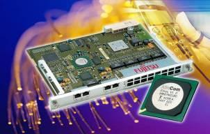
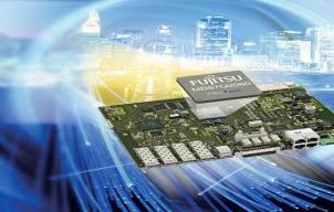
The Fujitsu 56GSa/s Analog-to-Digital Converter Enables 100GbE Transport
 The Fujitsu 56GSa/s Analog-to-Digital Converter Enables 100GbE Transport Ultra-fast CMOS Provides Technology Breakthrough for Upcoming Telecommunication Applications Technology Backgrounder Introduction
Micram DAC7201 and DAC GS/s Digital to Analog Converter Systems. Data Sheet
 Micram DAC7201 and DAC7202 72 GS/s Digital to Analog Converter s Data Sheet 72 GS/s Sample rate per channel 22+ GHz Analogue Bandwidth Very fast (
A 4 GSample/s 8-bit ADC in. Ken Poulton, Robert Neff, Art Muto, Wei Liu, Andrew Burstein*, Mehrdad Heshami* Agilent Laboratories Palo Alto, California
 A 4 GSample/s 8-bit ADC in 0.35 µm CMOS Ken Poulton, Robert Neff, Art Muto, Wei Liu, Andrew Burstein*, Mehrdad Heshami* Agilent Laboratories Palo Alto, California 1 Outline Background Chip Architecture
Signal Integrity Design of TSV-Based 3D IC
 Signal Integrity Design of TSV-Based 3D IC October 24, 21 Joungho Kim at KAIST joungho@ee.kaist.ac.kr http://tera.kaist.ac.kr 1 Contents 1) Driving Forces of TSV based 3D IC 2) Signal Integrity Issues
100 Gb/s: The High Speed Connectivity Race is On
 100 Gb/s: The High Speed Connectivity Race is On Cathy Liu SerDes Architect, LSI Corporation Harold Gomard SerDes Product Manager, LSI Corporation October 6, 2010 Agenda 100 Gb/s Ethernet evolution SoC
Low Jitter, Low Emission Timing Solutions For High Speed Digital Systems. A Design Methodology
 Low Jitter, Low Emission Timing Solutions For High Speed Digital Systems A Design Methodology The Challenges of High Speed Digital Clock Design In high speed applications, the faster the signal moves through
A 0.18µm SiGe BiCMOS Receiver and Transmitter Chipset for SONET OC-768 Transmission Systems
 A 0.18µm SiGe BiCMOS Receiver and Transmitter Chipset for SONET OC-768 Transmission Systems M. Meghelli 1, A. Rylyakov 1, S. J. Zier 2, M. Sorna 2, D. Friedman 1 1 IBM T. J. Watson Research Center 2 IBM
Measurement Results for a High Throughput MCM
 Measurement Results for a High Throughput MCM Funding: Paul Franzon Toby Schaffer, Alan Glaser, Steve Lipa North Carolina State University paulf@ncsu.edu www.ece.ncsu.edu/erl Outline > Heterogeneous System
ISSCC 2006 / SESSION 13 / OPTICAL COMMUNICATION / 13.2
 13.2 An MLSE Receiver for Electronic-Dispersion Compensation of OC-192 Fiber Links Hyeon-min Bae 1, Jonathan Ashbrook 1, Jinki Park 1, Naresh Shanbhag 2, Andrew Singer 2, Sanjiv Chopra 1 1 Intersymbol
A 10 bit, 1.8 GS/s Time Interleaved Pipeline ADC
 A 10 bit, 1.8 GS/s Time Interleaved Pipeline ADC M. Åberg 2, A. Rantala 2, V. Hakkarainen 1, M. Aho 1, J. Riikonen 1, D. Gomes Martin 2, K. Halonen 1 1 Electronic Circuit Design Laboratory Helsinki University
Microcircuit Electrical Issues
 Microcircuit Electrical Issues Distortion The frequency at which transmitted power has dropped to 50 percent of the injected power is called the "3 db" point and is used to define the bandwidth of the
Ultra-high-speed Interconnect Technology for Processor Communication
 Ultra-high-speed Interconnect Technology for Processor Communication Yoshiyasu Doi Samir Parikh Yuki Ogata Yoichi Koyanagi In order to improve the performance of storage systems and servers that make up
Development of a 20 GS/s Sampling Chip in 130nm CMOS Technology
 Development of a 20 GS/s Sampling Chip in 130nm CMOS Technology 2009 IEEE Nuclear Science Symposium, Orlando, Florida, October 28 th 2009 Jean-Francois Genat On behalf of Mircea Bogdan 1, Henry J. Frisch
FPGA based Prototyping of Next Generation Forward Error Correction
 Symposium: Real-time Digital Signal Processing for Optical Transceivers FPGA based Prototyping of Next Generation Forward Error Correction T. Mizuochi, Y. Konishi, Y. Miyata, T. Inoue, K. Onohara, S. Kametani,
Signal Integrity Modeling and Measurement of TSV in 3D IC
 Signal Integrity Modeling and Measurement of TSV in 3D IC Joungho Kim KAIST joungho@ee.kaist.ac.kr 1 Contents 1) Introduction 2) 2.5D/3D Architectures with TSV and Interposer 3) Signal integrity, Channel
Considerations in High-Speed High Performance Die-Package-Board Co-Design. Jenny Jiang Altera Packaging Department October 2014
 Considerations in High-Speed High Performance Die-Package-Board Co-Design Jenny Jiang Altera Packaging Department October 2014 Why Co-Design? Complex Multi-Layer BGA Package Horizontal and vertical design
FLYOVER QSFP APPLICATION DESIGN GUIDE
 FLYOVER QSFP APPLICATION DESIGN GUIDE FLY CRITICAL DATA OVER THE BOARD Samtec s Flyover QSFP Systems provide improved signal integrity and architectural flexibility by flying critical high-speed signals
EE434 ASIC & Digital Systems. Partha Pande School of EECS Washington State University
 EE434 ASIC & Digital Systems Partha Pande School of EECS Washington State University pande@eecs.wsu.edu Lecture 11 Physical Design Issues Interconnect Scaling Effects Dense multilayer metal increases coupling
on-chip Design for LAr Front-end Readout
 Silicon-on on-sapphire (SOS) Technology and the Link-on on-chip Design for LAr Front-end Readout Ping Gui, Jingbo Ye, Ryszard Stroynowski Department of Electrical Engineering Physics Department Southern
10.1: A 4 GSample/s 8b ADC in 0.35-um CMOS
 10.1: A 4 GSample/s 8b ADC in 0.35-um CMOS Ken Poulton, Robert Neff, Art Muto, Wei Liu*, Andy Burstein**, Mehrdad Heshami*** Agilent Technologies, Palo Alto, CA *Agilent Technologies, Colorado Springs,
Design Challenges in Multi-GHz Microprocessors
 Design Challenges in Multi-GHz Microprocessors Bill Herrick Director, Alpha Microprocessor Development www.compaq.com Introduction Moore s Law ( Law (the trend that the demand for IC functions and the
The Practical Limitations of S Parameter Measurements and the Impact on Time- Domain Simulations of High Speed Interconnects
 The Practical Limitations of S Parameter Measurements and the Impact on Time- Domain Simulations of High Speed Interconnects Dennis Poulin Anritsu Company Slide 1 Outline PSU Signal Integrity Symposium
High-speed Serial Interface
 High-speed Serial Interface Lect. 9 Noises 1 Block diagram Where are we today? Serializer Tx Driver Channel Rx Equalizer Sampler Deserializer PLL Clock Recovery Tx Rx 2 Sampling in Rx Interface applications
Another way to implement a folding ADC
 Another way to implement a folding ADC J. Van Valburg and R. van de Plassche, An 8-b 650 MHz Folding ADC, IEEE JSSC, vol 27, #12, pp. 1662-6, Dec 1992 Coupled Differential Pair J. Van Valburg and R. van
Electrical Characterization of a 64 Ball Grid Array Package
 EMC Europe - Hamburg, 8 th September 008 Summary Electrical Characterization of a 64 Ball Grid Array A. Boyer (), E. Sicard (), M. Fer (), L. Courau () () LATTIS - INSA of Toulouse - France () ST-Microelectronics
SV2C 28 Gbps, 8 Lane SerDes Tester
 SV2C 28 Gbps, 8 Lane SerDes Tester Data Sheet SV2C Personalized SerDes Tester Data Sheet Revision: 1.0 2015-03-19 Revision Revision History Date 1.0 Document release. March 19, 2015 The information in
A Fully Integrated 20 Gb/s Optoelectronic Transceiver Implemented in a Standard
 A Fully Integrated 20 Gb/s Optoelectronic Transceiver Implemented in a Standard 0.13 µm CMOS SOI Technology School of Electrical and Electronic Engineering Yonsei University 이슬아 1. Introduction 2. Architecture
P14155A: 128 Channel Cross-correlator ASIC Datasheet Rev 2.1
 SUMMARY P14155A is a cross-correlator ASIC, featuring a digital correlation matrix and on-chip 2-bit 1GS/s digitization of 128 analog inputs. Cross-correlation results in 4096 products plus 512 totalizers
Development of Radiation-Hard ASICs for the ATLAS Phase-1 Liquid Argon Calorimeter Readout Electronics Upgrade
 Development of Radiation-Hard ASICs for the ATLAS Phase-1 Liquid Argon Calorimeter Readout Electronics Upgrade Tim Andeen*, Jaroslav BAN, Nancy BISHOP, Gustaaf BROOIJMANS, Alex EMERMAN,Ines OCHOA, John
Preliminary Product Overview
 Preliminary Product Overview Features DC to > 3 GHz Frequency Range 25 Watt (CW), 200W (Pulsed) Max Power Handling Low On-State Insertion Loss, typical 0.3 db @ 3 GHz Low On-State Resistance < 0.75 Ω 25dB
Architectures and circuits for timeinterleaved. Sandeep Gupta Teranetics, Santa Clara, CA
 Architectures and circuits for timeinterleaved ADC s Sandeep Gupta Teranetics, Santa Clara, CA Outline Introduction to time-interleaved architectures. Conventional Sampling architectures and their application
Transmission-Line-Based, Shared-Media On-Chip. Interconnects for Multi-Core Processors
 Design for MOSIS Educational Program (Research) Transmission-Line-Based, Shared-Media On-Chip Interconnects for Multi-Core Processors Prepared by: Professor Hui Wu, Jianyun Hu, Berkehan Ciftcioglu, Jie
Micram DAC10001 and DAC GS/s Digital to Analog Converter System. Data Sheet
 Micram DAC10001 and DAC10002 100 GS/s Digital to Analog Converter Data Sheet 100 GS/s Sample rate per channel Single and Dual Channel s 35 GHz Analog Bandwidth (typical) Very fast (
Lecture 11: Clocking
 High Speed CMOS VLSI Design Lecture 11: Clocking (c) 1997 David Harris 1.0 Introduction We have seen that generating and distributing clocks with little skew is essential to high speed circuit design.
Proposing. An Interpolated Pipeline ADC
 Proposing An Interpolated Pipeline ADC Akira Matsuzawa Tokyo Institute of Technology, Japan Matsuzawa & Okada Lab. Background 38GHz long range mm-wave system Role of long range mm-wave Current Optical
The Design Challenge to Integrate High Performance Organic Packaging into High End ASIC Strategic Space Based Applications.
 The Design Challenge to Integrate High Performance Organic Packaging into High End ASIC Strategic Space Based Applications May 8, 2007 Abstract: The challenge to integrate high-end, build-up organic packaging
LSI and Circuit Technologies for the SX-8 Supercomputer
 LSI and Circuit Technologies for the SX-8 Supercomputer By Jun INASAKA,* Toshio TANAHASHI,* Hideaki KOBAYASHI,* Toshihiro KATOH,* Mikihiro KAJITA* and Naoya NAKAYAMA This paper describes the LSI and circuit
High Speed Characterization Report
 ERCD_020_XX_TTR_TED_1_D Mated with: ERF8-020-05.0-S-DV-L Description: 0.8mm Edge Rate High Speed Coax Cable Assembly Samtec, Inc. 2005 All Rights Reserved Table of Contents Cable Assembly Overview... 1
Lecture 160 Examples of CDR Circuits in CMOS (09/04/03) Page 160-1
 Page 160-1") Lecture 160 Examples of CDR Circuits in CMOS (09/04/03) Page 160-1 LECTURE 160 CDR EXAMPLES INTRODUCTION Objective The objective of this presentation is: 1.) Show two examples of clock and data recovery
Lecture 160 Examples of CDR Circuits in CMOS (09/04/03) Page 160-1 LECTURE 160 CDR EXAMPLES INTRODUCTION Objective The objective of this presentation is: 1.) Show two examples of clock and data recovery
Source: Nanju Na Jean Audet David R Stauffer IBM Systems and Technology Group
 Title: Package Model Proposal Source: Nanju Na (nananju@us.ibm.com) Jean Audet (jaudet@ca.ibm.com), David R Stauffer (dstauffe@us.ibm.com) Date: Dec 27 IBM Systems and Technology Group Abstract: New package
High Speed Characterization Report
 ESCA-XX-XX-XX.XX-1-3 Mated with: SEAF8-XX-05.0-X-XX-2-K SEAM8-XX-S02.0-X-XX-2-K Description: 0.80 mm SEARAY High-Speed/High-Density Array Cable Assembly, 34 AWG Samtec, Inc. 2005 All Rights Reserved Table
High Speed Characterization Report
 QTE-020-02-L-D-A Mated With QSE-020-01-L-D-A Description: Parallel Board-to-Board, 0.8mm Pitch, 8mm (0.315 ) Stack Height Samtec, Inc. 2005 All Rights Reserved Table of Contents Connector Overview... 1
Design Considerations for Highly Integrated 3D SiP for Mobile Applications
 Design Considerations for Highly Integrated 3D SiP for Mobile Applications FDIP, CA October 26, 2008 Joungho Kim at KAIST joungho@ee.kaist.ac.kr http://tera.kaist.ac.kr Contents I. Market and future direction
High-Performance Analog and RF Circuit Simulation using the Analog FastSPICE Platform at Columbia University. Columbia University
 High-Performance Analog and RF Circuit Simulation using the Analog FastSPICE Platform at Columbia University By: K. Tripurari, C. W. Hsu, J. Kuppambatti, B. Vigraham, P.R. Kinget Columbia University For
12 Bit 1.2 GS/s 4:1 MUXDAC
 RDA012M4 12 Bit 1.2 GS/s 4:1 MUXDAC Features 12 Bit Resolution 1.2 GS/s Sampling Rate 4:1 or 2:1 Input Multiplexer Differential Analog Output Input code format: Offset Binary Output Swing: 600 mv with
A 1.5 Gbps Transceiver Chipset in 0.13-mm CMOS for Serial Digital Interface
 JOURNAL OF SEMICONDUCTOR TECHNOLOGY AND SCIENCE, VOL.17, NO.4, AUGUST, 2017 ISSN(Print) 1598-1657 https://doi.org/10.5573/jsts.2017.17.4.552 ISSN(Online) 2233-4866 A 1.5 Gbps Transceiver Chipset in 0.13-mm
EVALUATION KIT AVAILABLE +3.3V, Low-Jitter Crystal to LVPECL Clock Generator QA_C. 125MHz QA QA. 125MHz MAX3679A QB0 QB MHz QB1 QB
 19-4858; Rev 0; 8/09 EVALUATION KIT AVAILABLE +3.3V, Low-Jitter Crystal to LVPECL General Description The is a low-jitter precision clock generator with the integration of three LVPECL and one LVCMOS outputs
Low Power DSP and Photonic Integration in Optical Networks. Atul Srivastava CTO, NTT Electronics - America. Market Focus ECOC 2014
 Low Power DSP and Photonic Integration in Optical Networks Atul Srivastava CTO, NTT Electronics - America Market Focus ECOC 2014 Outline 100G Deployment Rapid Growth in Long Haul Role of Modules New Low
AD9300 SPECIFICATIONS ELECTRICAL CHARACTERISTICS ( V S = 12 V 5%; C L = 10 pf; R L = 2 k, unless otherwise noted) COMMERCIAL 0 C to +70 C Test AD9300K
 COMMERCIAL 0 C to +70 C Test AD9300K") a FEATURES 34 MHz Full Power Bandwidth 0.1 db Gain Flatness to 8 MHz 72 db Crosstalk Rejection @ 10 MHz 0.03 /0.01% Differential Phase/Gain Cascadable for Switch Matrices MIL-STD-883 Compliant Versions
a FEATURES 34 MHz Full Power Bandwidth 0.1 db Gain Flatness to 8 MHz 72 db Crosstalk Rejection @ 10 MHz 0.03 /0.01% Differential Phase/Gain Cascadable for Switch Matrices MIL-STD-883 Compliant Versions
ECEN689: Special Topics in High-Speed Links Circuits and Systems Spring 2012
 ECEN689: Special Topics in High-Speed Links Circuits and Systems Spring 2012 Lecture 5: Termination, TX Driver, & Multiplexer Circuits Sam Palermo Analog & Mixed-Signal Center Texas A&M University Announcements
3D IC-Package-Board Co-analysis using 3D EM Simulation for Mobile Applications
 3D IC-Package-Board Co-analysis using 3D EM Simulation for Mobile Applications Darryl Kostka, CST of America Taigon Song and Sung Kyu Lim, Georgia Institute of Technology Outline Introduction TSV Array
Fractional- N PLL with 90 Phase Shift Lock and Active Switched- Capacitor Loop Filter
 J. Park, F. Maloberti: "Fractional-N PLL with 90 Phase Shift Lock and Active Switched-Capacitor Loop Filter"; Proc. of the IEEE Custom Integrated Circuits Conference, CICC 2005, San Josè, 21 September
ICS2510C. 3.3V Phase-Lock Loop Clock Driver. Integrated Circuit Systems, Inc. General Description. Pin Configuration.
 Integrated Circuit Systems, Inc. ICS250C 3.3V Phase-Lock Loop Clock Driver General Description The ICS250C is a high performance, low skew, low jitter clock driver. It uses a phase lock loop (PLL) technology
Synchronous Mirror Delays. ECG 721 Memory Circuit Design Kevin Buck
 Synchronous Mirror Delays ECG 721 Memory Circuit Design Kevin Buck 11/25/2015 Introduction A synchronous mirror delay (SMD) is a type of clock generation circuit Unlike DLLs and PLLs an SMD is an open
Basic Functional Analysis. Sample Report Richmond Road, Suite 500, Ottawa, ON K2H 5B7 Canada Tel:
 Basic Functional Analysis Sample Report 3685 Richmond Road, Suite 500, Ottawa, ON K2H 5B7 Canada Tel: 613-829-0414 www.chipworks.com Basic Functional Analysis Sample Report Some of the information in this
Note Using the PXIe-5785 in a manner not described in this document might impair the protection the PXIe-5785 provides.
 SPECIFICATIONS PXIe-5785 PXI FlexRIO IF Transceiver This document lists the specifications for the PXIe-5785. Specifications are subject to change without notice. For the most recent device specifications,
A 10Gbps Analog Adaptive Equalizer and Pulse Shaping Circuit for Backplane Interface
 Proceedings of the 5th WSEAS Int. Conf. on CIRCUITS, SYSTEMS, ELECTRONICS, CONTROL & SIGNAL PROCESSING, Dallas, USA, November 1-3, 2006 225 A 10Gbps Analog Adaptive Equalizer and Pulse Shaping Circuit
Pipeline vs. Sigma Delta ADC for Communications Applications
 Pipeline vs. Sigma Delta ADC for Communications Applications Noel O Riordan, Mixed-Signal IP Group, S3 Semiconductors noel.oriordan@s3group.com Introduction The Analog-to-Digital Converter (ADC) is a key
DESIGN OF A 500MHZ, 4-BIT LOW POWER ADC FOR UWB APPLICATION
 DESIGN OF A 500MHZ, 4-BIT LOW POWER ADC FOR UWB APPLICATION SANTOSH KUMAR PATNAIK 1, DR. SWAPNA BANERJEE 2 1,2 E & ECE Department, Indian Institute of Technology, Kharagpur, Kharagpur, India Abstract-This
High Speed Characterization Report
 SSW-1XX-22-X-D-VS Mates with TSM-1XX-1-X-DV-X Description: Surface Mount Terminal Strip,.1 [2.54mm] Pitch, 13.59mm (.535 ) Stack Height Samtec, Inc. 25 All Rights Reserved Table of Contents Connector Overview...
LSI and Circuit Technologies of the SX-9
 TANAHASHI Toshio, TSUCHIDA Junichi, MATSUZAWA Hajime NIWA Kenji, SATOH Tatsuo, KATAGIRI Masaru Abstract This paper outlines the LSI and circuit technologies of the SX-9 as well as their inspection technologies.
High Speed Characterization Report
 QTH-030-01-L-D-A Mates with QSH-030-01-L-D-A Description: High Speed Ground Plane Header Board-to-Board, 0.5mm (.0197 ) Pitch, 5mm (.1969 ) Stack Height Samtec, Inc. 2005 All Rights Reserved Table of Contents
Synthesis of Optimal On-Chip Baluns
 Synthesis of Optimal On-Chip Baluns Sharad Kapur, David E. Long and Robert C. Frye Integrand Software, Inc. Berkeley Heights, New Jersey Yu-Chia Chen, Ming-Hsiang Cho, Huai-Wen Chang, Jun-Hong Ou and Bigchoug
EA/MZ Modulator Driver PMCC_EAMD12G
 EA/MZ Modulator Driver PMCC_EAMD12G IP MACRO Datasheet Rev 1.0 Process: Jazz Semiconductor SBC18HX DESCRIPTIO The PMCC_EAMD12G is designed to directly drive the 50Ω inputs of EA or MZ Modulators or EML
/$ IEEE
 IEEE TRANSACTIONS ON CIRCUITS AND SYSTEMS II: EXPRESS BRIEFS, VOL. 53, NO. 11, NOVEMBER 2006 1205 A Low-Phase Noise, Anti-Harmonic Programmable DLL Frequency Multiplier With Period Error Compensation for
ECEN 720 High-Speed Links: Circuits and Systems
 1 ECEN 720 High-Speed Links: Circuits and Systems Lab4 Receiver Circuits Objective To learn fundamentals of receiver circuits. Introduction Receivers are used to recover the data stream transmitted by
Low-Jitter, Precision Clock Generator with Two Outputs
 19-2456; Rev 0; 11/07 E V A L U A T I O N K I T A V A I L A B L E Low-Jitter, Precision Clock Generator Ethernet Networking Equipment General Description The is a low-jitter precision clock generator optimized
HIFAS: Wide-band spectrometer ASIC
 HIFAS: Wide-band spectrometer ASIC Anders Emrich, Stefan Andersson, Johan Dahlberg, Magnus Hjorth, Omnisys Instruments AB Torgil Kjellberg, Chalmers University Of Technology Microelectronics Presentation
A 4 Channel Waveform Sampling ASIC in 130 nm CMOS
 A 4 Channel Waveform Sampling ASIC in 130 nm CMOS E. Oberla, H. Grabas, J.F. Genat, H. Frisch Enrico Fermi Institute, University of Chicago K. Nishimura, G. Varner University of Hawai I Large Area Picosecond
PCB Design Guidelines for GPS chipset designs. Section 1. Section 2. Section 3. Section 4. Section 5
 PCB Design Guidelines for GPS chipset designs The main sections of this white paper are laid out follows: Section 1 Introduction Section 2 RF Design Issues Section 3 Sirf Receiver layout guidelines Section
SiNANO-NEREID Workshop:
 SiNANO-NEREID Workshop: Towards a new NanoElectronics Roadmap for Europe Leuven, September 11 th, 2017 WP3/Task 3.2 Connectivity RF and mmw Design Outline Connectivity, what connectivity? High data rates
Accomplishment and Timing Presentation: Clock Generation of CMOS in VLSI
 Accomplishment and Timing Presentation: Clock Generation of CMOS in VLSI Assistant Professor, E Mail: manoj.jvwu@gmail.com Department of Electronics and Communication Engineering Baldev Ram Mirdha Institute
A 2-bit/step SAR ADC structure with one radix-4 DAC
 A 2-bit/step SAR ADC structure with one radix-4 DAC M. H. M. Larijani and M. B. Ghaznavi-Ghoushchi a) School of Engineering, Shahed University, Tehran, Iran a) ghaznavi@shahed.ac.ir Abstract: In this letter,
77 GHz VCO for Car Radar Systems T625_VCO2_W Preliminary Data Sheet
 77 GHz VCO for Car Radar Systems Preliminary Data Sheet Operating Frequency: 76-77 GHz Tuning Range > 1 GHz Output matched to 50 Ω Application in Car Radar Systems ESD: Electrostatic discharge sensitive
UT90nHBD Hardened-by-Design (HBD) Standard Cell Data Sheet February
 Standard Cell Data Sheet February") Semicustom Products UT90nHBD Hardened-by-Design (HBD) Standard Cell Data Sheet February 2018 www.cobham.com/hirel The most important thing we build is trust FEATURES Up to 50,000,000 2-input NAND equivalent
Semicustom Products UT90nHBD Hardened-by-Design (HBD) Standard Cell Data Sheet February 2018 www.cobham.com/hirel The most important thing we build is trust FEATURES Up to 50,000,000 2-input NAND equivalent
HA4600. Features. 480MHz, SOT-23, Video Buffer with Output Disable. Applications. Pinouts. Ordering Information. Truth Table
 TM Data Sheet June 2000 File Number 3990.6 480MHz, SOT-23, Video Buffer with Output Disable The is a very wide bandwidth, unity gain buffer ideal for professional video switching, HDTV, computer monitor
Multiple Reference Clock Generator
 A White Paper Presented by IPextreme Multiple Reference Clock Generator Digitial IP for Clock Synthesis August 2007 IPextreme, Inc. This paper explains the concept behind the Multiple Reference Clock Generator
Noise on Vcc Webinar. Presenters: Vitali Penso, Applications Engineer Murat Eron, VP of Engineering. Page 1
 Noise on Vcc Webinar Presenters: Vitali Penso, Applications Engineer Murat Eron, VP of Engineering Page 1 Webinar Agenda Noise on Vcc Major sources of IC chip interference Susceptible Device Types Example
IP Specification. 12-Bit 125 MSPS Duel ADC in SMIC40L IPS_S40L_ADC12X2_125M FEATURES APPLICATIONS GENERAL DESCRIPTION. Single Supply 1.
 12-Bit 125 MSPS Duel ADC in SMIC40L FEATURES Single Supply 1.15V 125 MSPS Conversion Rate AVDD AVSS VDD VSS Current Consumption 45 mw @ 125 MSPS Dynamic Performance @ 125MSPS 65 dbfs SNR -68 dbc THD 70
SERDES Reference Clock
 April 2003 Technical Note TN1040 Introduction This document discusses the ORT82G5, ORT42G5, ORSO82G5 and ORSO42G5 FPSC devices [1] reference clock input characteristics and the selection/interconnection
Engineering the Power Delivery Network
 C HAPTER 1 Engineering the Power Delivery Network 1.1 What Is the Power Delivery Network (PDN) and Why Should I Care? The power delivery network consists of all the interconnects in the power supply path
Chapter 16 PCB Layout and Stackup
 Chapter 16 PCB Layout and Stackup Electromagnetic Compatibility Engineering by Henry W. Ott Foreword The PCB represents the physical implementation of the schematic. The proper design and layout of a printed
Power Distribution Network Design for Stratix IV GX and Arria II GX FPGAs
 Power Distribution Network Design for Stratix IV GX and Arria II GX FPGAs Transceiver Portfolio Workshops 2009 Question What is Your PDN Design Methodology? Easy Complex Historical Full SPICE simulation
Section 1. Fundamentals of DDS Technology
 Section 1. Fundamentals of DDS Technology Overview Direct digital synthesis (DDS) is a technique for using digital data processing blocks as a means to generate a frequency- and phase-tunable output signal
FIRST TELECOM APPLICATION OF DIGITAL AND MIXED COMPONENT DEVELOPMENTS: 65NM ASIC AND DATA CONVERTERS
 AMICSA 2016 FIRST TELECOM APPLICATION OF DIGITAL AND MIXED COMPONENT DEVELOPMENTS: 65NM ASIC AND DATA CONVERTERS F. MALOU, C. AMIOT-BAZILE (CNES), P. VOISIN (TAS) 15th June, 2016 1 Outline FAST project
Phase-Locked Loops and Their Applications. Advanced PLL Examples (Part II)
") Short Course On Phase-Locked Loops and Their Applications Day 5, PM Lecture Advanced PLL Examples (Part II) Michael Perrott August 15, 2008 Copyright 2008 by Michael H. Perrott All rights reserved. Outline
Short Course On Phase-Locked Loops and Their Applications Day 5, PM Lecture Advanced PLL Examples (Part II) Michael Perrott August 15, 2008 Copyright 2008 by Michael H. Perrott All rights reserved. Outline
5Gbps Serial Link Transmitter with Pre-emphasis
 Gbps Serial Link Transmitter with Pre-emphasis Chih-Hsien Lin, Chung-Hong Wang and Shyh-Jye Jou Department of Electrical Engineering,National Central University,Chung-Li, Taiwan R.O.C. Abstract- High-speed
High Speed Characterization Report
 ECDP-16-XX-L1-L2-2-2 Mated with: HSEC8-125-XX-XX-DV-X-XX Description: High-Speed 85Ω Differential Edge Card Cable Assembly, 30 AWG ACCELERATE TM Twinax Cable Samtec, Inc. 2005 All Rights Reserved Table
Impact of On-Chip Multi-Layered Inductor on Signal and Power Integrity of Underlying Power-Ground Net
 22 nd IEEE Workshop on Signal and Power Integrity, Brest, FRANCE May 25, 2018 Impact of On-Chip Multi-Layered Inductor on Signal and Power Integrity of Underlying Power-Ground Net Akira Tsuchicya 1, Akitaka
Clock Tree 101. by Linda Lua
 Tree 101 by Linda Lua Table of Contents I. What is a Tree? II. III. Tree Components I. Crystals and Crystal Oscillators II. Generators III. Buffers IV. Attenuators versus Crystal IV. Free-running versus
Low-Jitter, 8kHz Reference Clock Synthesizer Outputs MHz
 19-3530; Rev 0; 1/05 Low-Jitter, 8kHz Reference General Description The low-cost, high-performance clock synthesizer with an 8kHz input reference clock provides six buffered LVTTL clock outputs at 35.328MHz.
Relationship Between Signal Integrity and EMC
 Relationship Between Signal Integrity and EMC Presented by Hasnain Syed Solectron USA, Inc. RTP, North Carolina Email: HasnainSyed@solectron.com 06/05/2007 Hasnain Syed 1 What is Signal Integrity (SI)?
Reducing Development Risk in Communications Applications with High-Performance Oscillators
 V.7/17 Reducing Development Risk in Communications Applications with High-Performance Oscillators Introducing Silicon Labs new Ultra Series TM Oscillators Powered by 4 th Generation DSPLL Technology, new
Maximizing GSPS ADC SFDR Performance: Sources of Spurs and Methods of Mitigation
 Maximizing GSPS ADC SFDR Performance: Sources of Spurs and Methods of Mitigation Marjorie Plisch Applications Engineer, Signal Path Solutions November 2012 1 Outline Overview of the issue Sources of spurs
1.25Gbps/2.5Gbps, +3V to +5.5V, Low-Noise Transimpedance Preamplifiers for LANs
 19-4796; Rev 1; 6/00 EVALUATION KIT AVAILABLE 1.25Gbps/2.5Gbps, +3V to +5.5V, Low-Noise General Description The is a transimpedance preamplifier for 1.25Gbps local area network (LAN) fiber optic receivers.
High Speed Digital Design & Verification Seminar. Measurement fundamentals
 High Speed Digital Design & Verification Seminar Measurement fundamentals Agenda Sources of Jitter, how to measure and why Importance of Noise Select the right probes! Capture the eye diagram Why measure
A 42 fj 8-bit 1.0-GS/s folding and interpolating ADC with 1 GHz signal bandwidth
 LETTER IEICE Electronics Express, Vol.11, No.2, 1 9 A 42 fj 8-bit 1.0-GS/s folding and interpolating ADC with 1 GHz signal bandwidth Mingshuo Wang a), Fan Ye, Wei Li, and Junyan Ren b) State Key Laboratory
High Speed Characterization Report
 PCIEC-XXX-XXXX-EC-EM-P Mated with: PCIE-XXX-02-X-D-TH Description: 1.00 mm PCI Express Internal Cable Assembly, 30 AWG Twinax Ribbon Cable Samtec, Inc. 2005 All Rights Reserved Table of Contents Cable
7 GHz INTEGER N SYNTHESIZER CONTINUOUS (N = ), NON-CONTINUOUS (N = 16-54) Features
, NON-CONTINUOUS (N = 16-54) Features") HMC99LP5 / 99LP5E CONTINUOUS (N = 5-519), NON-CONTINUOUS (N = 1-54) Typical Applications The HMC99LP5(E) is ideal for: Satellite Communication Systems Point-to-Point Radios Military Applications Sonet
HMC99LP5 / 99LP5E CONTINUOUS (N = 5-519), NON-CONTINUOUS (N = 1-54) Typical Applications The HMC99LP5(E) is ideal for: Satellite Communication Systems Point-to-Point Radios Military Applications Sonet
Analogue circuit design for RF immunity
 Analogue circuit design for RF immunity By EurIng Keith Armstrong, C.Eng, FIET, SMIEEE, www.cherryclough.com First published in The EMC Journal, Issue 84, September 2009, pp 28-32, www.theemcjournal.com