Setting Up. IC-CAP WaferPro. For On-Wafer Measurements
|
|
|
- Allyson Taylor
- 5 years ago
- Views:
Transcription

1 Setting Up IC-CAP WaferPro For On-Wafer Measurements Copyright Agilent Technologies
2 Contents - What Is WaferPro - A Typical Lab Environment For WaferPro - The WaferPro User Interface Concept - WaferPro Measurement Data Structure - Setting Up A Test Plan For A Demo Wafer - WaferPro And S-Parameters Conclusions 2

3 What is WaferPro? It is an IC-CAP Module, with a specific user interface, on top of the IC-CAP Framework, which > sets the ThermoChuck temperature > controls the prober and provides the Probes/ProbeCard contact > switches the matrix and then lets the user apply all kinds of measurements, applying all the flexibility of a standard IC-CAP session. It outputs the measurement data in a directory/file structure (.mdm), or into a SQL data base (next IC-CAP release). 3

 WaferPro User Interface (myproject.")
4 IC-CAP WaferPro Architecture Overview Start WaferPro see also the next slide... IC-CAP Environment (wprolibrary.mdl) WaferPro User Interface (myproject.xml) 4
 IC-CAP Product Numbers: -> WaferPro User Interface (GUI) W8510EP WaferPro 85199A IC-CAP Framework 85199D DC Drivers 85199C CV Drivers 85199E NWA Drivers (optional)")
5 IC-CAP WaferPro Architecture Overview (cont'd) The WaferPro Module consists of 3 parts: -> ModelFile 'Routine' (DUTs/Setups with DC,CV, Spar Measurement Tasks) -> ModelFile 'Driver' (control of WaferProber, Matrix, ThermoChuck) IC-CAP Product Numbers: -> WaferPro User Interface (GUI) W8510EP WaferPro 85199A IC-CAP Framework 85199D DC Drivers 85199C CV Drivers 85199E NWA Drivers (optional) 85199B Simul.Interface (optional) 1.) User Interface 2.) Wafer Prober Switching Matrix Thermochuck 3.) Measurement Setups Notes: the module W8510EP requires an existing IC-CAP installation, while the Bundle W8511BP includes modules 85199A, 85199C, 85199D, 85199E, W8510EP, i.e. a complete IC-CAP. 5


6 IC-CAP and therefore also WaferPro distinguish between 'real' measurement instruments (ModelFile 'Routine') e.g. DC analyzer, CV meter etc. and auxiliary instruments (ModelFile 'Driver') like ThermoChuck, WaferProber and SwitchingMatrix if required, add here drivers for you prober, matrix, chuck if required, add here your measurement setups 6
7 Contents - What Is WaferPro - A Typical Lab Environment For WaferPro - The WaferPro User Interface Concept - WaferPro Measurement Data Structure - Setting Up A Test Plan For A Demo Wafer - WaferPro And S-Parameters Conclusions 7


8 A Typical Lab Environment for WaferPro WaferPro Individual Measurement Benches with different Probers/Matrices/Instruments Production Bench Prober Fully Automated Prober (incl. Wafer Cassette) Matrix CV Meter DC Analyzer DC&CV Parametric Test System incl. Switching Matrix Page 8 8

9 WaferPro allows to apply your Test Plan to any available Bench, by simply selecting the Bench Name Bench1 Bench 2 Bench 3 Bench1 Bench2 Bench3... in other words... you can apply your Test Plan without any changes, immediately to any of your Benches! 9
10 ... another application of WaferPro is when you have older GPIB-controlled wafer probers, but no state-of-the-art, common user interface available... 10
11 Contents - What Is WaferPro - A Typical Lab Environment For WaferPro - The WaferPro User Interface Concept - WaferPro Measurement Data Structure - Setting Up A Test Plan For A Demo Wafer - WaferPro And S-Parameters Conclusions 11


12 The WaferPro User Interface Concept which device types (diodes, transistors, resistors etc.) which measurement system to use? what is available on the wafer? which meas.candidates? which bias conditions? define the test plan: group meas. candidates and conditions Go! Meas.Results.mdm or Database 12

13 Step by step... Bench1 Bench 2 Bench 3 Select which Bench to use 13


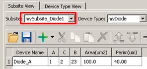
14 Enter the Wafer Geometry and the Die size Specify the Subsites Set up the Device Definition Table 14
15 Setting Up the Test Plan Setting Up the Test Plan in WaferPro means - define what is available (devices and their meas. types and meas. conditions) - build groups of tasks - perform the wafer test 15
16 In the following slides, we will discuss the definitions of the test possibilities, followed by setting up groups of tasks, to be performed during the 'Test Plan Run' 16

17 1. lists of dies 1. 17
18 lists of subsite devices lists of dies
19 list of meas. routines 3. lists of meas. conditions for the meas. routines lists of meas ranges lists of dies lists of subsite devices 3. 19

20 list of meas. routines lists of meas. conditions for the meas. routines lists of meas ranges lists of dies lists of subsite devices build lists of devices, measurements types meas. conditions 20


, temperature,")
21 list of meas. routines lists of meas. conditions for the meas. routines lists of meas ranges lists of dies lists of subsite devices build lists of devices, measurements types meas. conditions build lists of wafer(s), temperature, target dies and characterization steps 21
22 GO! 22


23 Lot Wafers Dies Technology Definition Blocks Subsites Devices Wrap-Up WaferPro Flow Measurement Definition Characterization Step Test Plan Sequence: Temp, Wafer, Die List, Characterization Steps Go! 23
24 Contents - What Is WaferPro - A Typical Lab Environment For WaferPro - The WaferPro User Interface Concept - WaferPro Measurement Data Structure - Setting Up A Test Plan For A Demo Wafer - WaferPro And S-Parameters Conclusions 24
25 WaferPro Measurement Data Structure 25
26 Contents - What Is WaferPro - A Typical Lab Environment For WaferPro - The WaferPro User Interface Concept - WaferPro Measurement Data Structure - Setting Up A Test Plan For A Demo Wafer - WaferPro And S-Parameters Conclusions 26

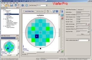
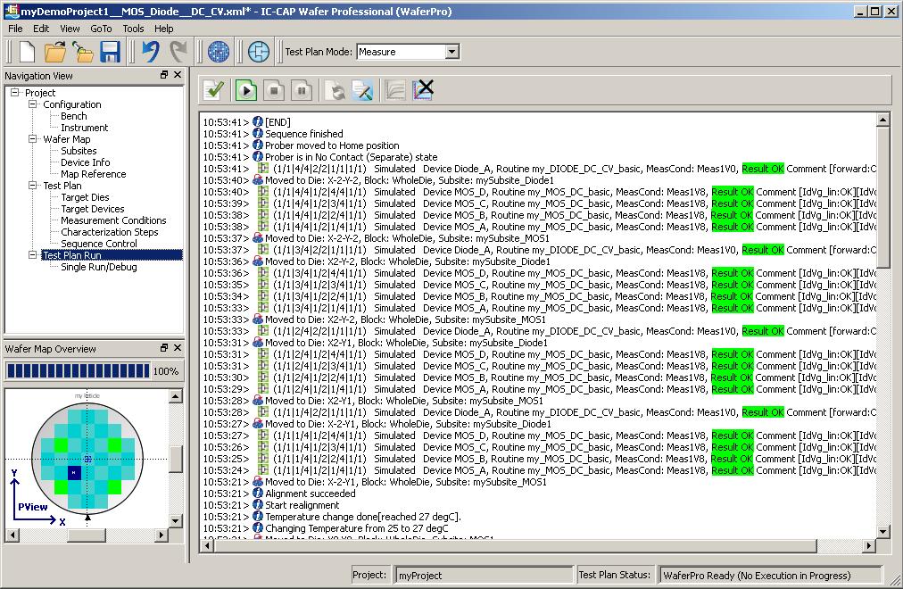
27 Setting up a Test Plan for a Demo Wafer A Simple WaferPro Example This and the following slides can be found in $ICCAP_ROOT/WaferPro/examples/documentation_pdf/1_WaferPro_GettingStarted_ pdf The corresponding WaferPro file is: $ICCAP_ROOT/WaferPro/examples/myDemoProject1 MOS_Diode DC_CV.xml 27
28 Describing the Wafer(s), Dies and Devices in the WaferPro GUI... 28

29 Selecting Our Demo Bench Note for IC-CAP users: this selection specifies the IC-CAP 'mydemo_4142_4275.hdw' file plus in the WaferPro wprobenchlist.cfg file the entry 'mydemo_4142_4275' 29

30 Verifying/Defining the Measurement Setups in the IC-CAP environment... 30

31 - In the IC-CAP ModelFile 'Routine', we define a group (DUT) called 'my_mos_dc_basics' and a group (DUT) 'my_diode_dc_cv_basic'. - We can add as many Setups to each group, depending on our planned measurements. The only prerequisite is to have the 3 Specific-Names-Transforms defined. These 3 Transforms are the jumping points for WaferPro IMPORTANT WaferPro FEATURE: Your PEL Programs can communicate with the WaferPro settings, applying the PEL Functions - WPro_set_info(): PEL -> WaferPro - WPro_lookup_info(): WaferPro -> PEL 31


32 Routine ModelFile WaferPro For the measurement conditions, we apply variables, which are set by WaferPro. This allows to re-use our Setups for different technologies 32


33 Our Demo Wafer 5 inch (=127mm diameter) Die 15mm x 16mm 16mm 15mm Wafer Orientation Flat Subsite (probe card contact) 33


34 Entering the Demo Wafer Details into WaferPro 34

35 The Dies and their Subsites on our Demo Wafer MOS1 Subsite x=0mm, y=12mm 15mm 16mm Diode1 Subsite x=9mm, y=11mm Wafer Flat Orientation 35


36 Defining the Die Subsites locations in WaferPro 36
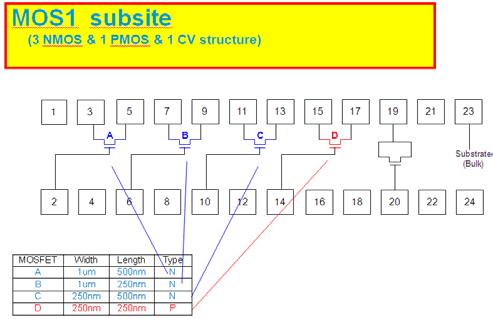
 370um 2 4 6 8 10 12 14 16 18 20 22 24 MOSFET Width Length Type A 1um 500nm N B 1um 250nm N C 250nm 500nm N D 250nm")
37 MOS1 subsite (3 NMOS & 1 PMOS & 1 CV structure) 120um 35um 120um 130um A B C D Substrate (Bulk) 370um MOSFET Width Length Type A 1um 500nm N B 1um 250nm N C 250nm 500nm N D 250nm 250nm P 37
38 Diode1 subsite (2 devices, DC & CV measurement) 120um 35um 120um um Diode_A Substrate (Bulk) 370um

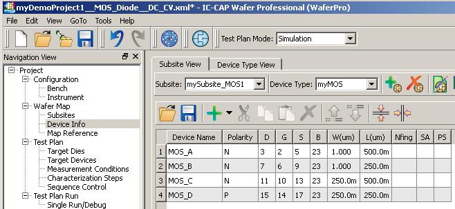
39 Setting Up the Device Definition Tables (pins, geometry, polarity, etc.) 39

40 Defining Lists of Die Test Candidates tbd 40


41 Defining Lists of Subsite Test Candidates 41
 to different technologies!")
42 Defining Lists of Measurement Conditions Note: you can apply the same test (the IC-CAP Setup in ModelFile 'Routine') to different technologies! 42


43 From the previously defined information, build Lists of Subsites, how to Measure then and what Meas. Limits to apply 43
44 Finally, Setting Up Groups of Tasks from the available Lists 44

45 Executing the Test Plan 45
46 Contents - What Is WaferPro - A Typical Lab Environment For WaferPro - The WaferPro User Interface Concept - WaferPro Measurement Data Structure - Setting Up A Test Plan For A Demo Wafer - WaferPro And S-Parameters Conclusions 46

47 Layout Sketch of our Demo Devices and entering this info into the WaferPro GUI y Die 600um ThruDummy Subsites 400um ShortDummy 200um OpenDummy NPN_A 200um NPN_B x 47


48 If not yet available, add the new Device Type(s) to WaferPro 48

 and call the Spar nodes P1 and P2.")

49 Set Up Measurements in ModelFile /Routine in WaferPro's Modelfile /Routine, add a new DUT, here called 'my_npn_basic' -> like it is best practice with IC-CAP, name the DC and CV nodes after the transistor pin names (e.g. C, B, E, S for a bipolar transistor) and call the Spar nodes P1 and P2. DC Spar Note: we group the transistor and the de-embedding dummies within the same /Routine/DUT, so that we can apply DUT-Variables 'fmin', 'fmax' and 'fpts' for all Spar Setups. 49

50 Define the fixed SMU connections (SMU<->NWA cabling) in WaferPro enter here your cablings Very Important: The SMU connections defined here will overwrite the ones specified in the /Routine Setups!!! Reason: this allows to switch from bench to bench without manipulating the /Routine Setups!! 50
:")

51 WaferPro: Sequence Control Make sure to correctly specify the sequence of Char.Steps: first the de-embedding dummies, then the transistors Reason (best practice): When the transistor will be measured, the dummies have been measured already, and we can apply a simple de-embedding without loading first the.mdm files of the de-embedding dummies! 51
52 For more details, see the documentation in $ICCAP_ROOT/ 52
53 Contents - What Is WaferPro - A Typical Lab Environment For WaferPro - The WaferPro User Interface Concept - WaferPro Measurement Data Structure - Setting Up A Test Plan For A Demo Wafer - WaferPro And S-Parameters Conclusions 53
54 IC-CAP WaferPro Is An Extremely Powerful Test Plan Suite, For On-Wafer DC/CV And RF Device Modeling Measurements. It supports a variety of thermo chucks, wafer probers, matrices and instruments, including the Agilent parametric testers. Own drivers can be added easily. It includes several built-in measurement routines, which are nevertheless open for users to customize or enhance the measurement and post-processing. It will be compatible with a new IC-CAP Database feature and provide the foundation for advanced Statistical Modeling. 54
55 Where To Find More Information IC-CAP WaferPro Webpage: WaferPro White Paper: IC-CAP Device Modeling Software: Latest IC-CAP Demos see the IC-CAP KnowledgeCenter at: ersion) Device Modeling Handbook see 55
56 Thank you for your attention! 56
Welcome! Device Characterization with the Keithley Model 4200-SCS Characterization System.
 Welcome! Device Characterization with the Keithley Model 4200-SCS Characterization System Safety Precautions Working with Electricity Before starting, check cables for cracks or wear. Get new cables if
Agilent 4070 Series Accurate Capacitance Characterization at the Wafer Level
 Agilent 4070 Series Accurate Capacitance Characterization at the Wafer Level Application Note 4070-2 Agilent 4070 Series Semiconductor Parametric Tester Introduction The continuing trend of decreasing
A NEW DC MEASUREMENT PRINCIPLE TO FULLY COVER DEVICE SELF-HEATING
 -1- A NEW DC MEASUREMENT PRINCIPLE TO FULLY COVER DEVICE SELF-HEATING Keywords: Device Self-Heating During DC Measurement, Data Sampling After Self-Heating Reached Final Value, IC-CAP Demo File Contents:
A Unique System Concept to Improve the Accuracy of Wafer-Level Flicker-Noise Characterization. Andrej Rumiantsev, Stojan Kanev
 A Unique System Concept to Improve the Accuracy of Wafer-Level Flicker-Noise Characterization Andrej Rumiantsev, Stojan Kanev Content Motivation Challenges for 1/f Measurements New Probe System Concept
BJT Characterization Laboratory Dr. Lynn Fuller
 ROCHESTER INSTITUTE OF TECHNOLOGY MICROELECTRONIC ENGINEERING BJT Characterization Laboratory Dr. Lynn Fuller 82 Lomb Memorial Drive Rochester, NY 14623-5604 Tel (585) 475-2035 Fax (585) 475-5041 Email:
S540 Power Semiconductor Test System Datasheet
 S540 Power Semiconductor Test System Datasheet Key Features Automatically perform all wafer-level parametric tests on up to 48 pins, including high voltage breakdown, capacitance, and low voltage measurements,
Agilent 4083A DC/RF Parametric Test System A fully automatic on-wafer RF S-parameter measurement environment
 Agilent 4083A DC/RF Parametric Test System A fully automatic on-wafer RF S-parameter measurement environment Application Note 4080-2 Introduction The current telecommunications revolution rests upon myriad
Agilent 4072A Advanced Parametric Test System with Agilent SPECS
 Agilent 4072A Advanced Parametric Test System with Agilent SPECS Technical Data 1. General Description The Agilent 4072A Advanced Parametric Test System is designed to perform precision DC measurement,
Ridgetop Group, Inc.
 Ridgetop Group, Inc. Ridgetop Group Facilities in Tucson, AZ Arizona-based firm, founded in 2000, with focus on electronics for critical applications Two divisions: Semiconductor & Precision Instruments
S540 Power Semiconductor Test System Datasheet
 S540 Power Semiconductor Test System Key Features Automatically perform all wafer-level parametric tests on up to 48 pins, including high voltage breakdown, capacitance, and low voltage measurements, in
End-of-line Standard Substrates For the Characterization of organic
 FRAUNHOFER INSTITUTe FoR Photonic Microsystems IPMS End-of-line Standard Substrates For the Characterization of organic semiconductor Materials Over the last few years, organic electronics have become
EE 230 Lab Lab 9. Prior to Lab
 MOS transistor characteristics This week we look at some MOS transistor characteristics and circuits. Most of the measurements will be done with our usual lab equipment, but we will also use the parameter
Lecture 8. MOS Transistors; Cheap Computers; Everycircuit
 Lecture 8 MOS Transistors; Cheap Computers; Everycircuit Copyright 2017 by Mark Horowitz 1 Reading The rest of Chapter 4 in the reader For more details look at A&L 5.1 Digital Signals (goes in much more
Positioning S-Parameters, Harmonic Measurements and X-Parameters for Device Modeling ADS
 Slide Positioning S-Parameters, Harmonic and X-Parameters for Device Modeling Devices, Circuits ADS IC-CAP NVNA Franz.Sischka@Agilent.com Slide 2 PNA-X Agenda VNA. S-Parameter 2. Harmonic NVNA 3. X-Parameter
Electrostatic Test Structures for Transmission Line Pulse and Human Body Model Testing at Wafer Level
 Electrostatic Test Structures for Transmission Line Pulse and Human Body Model Testing at Wafer Level Robert Ashton 1, Stephen Fairbanks 2, Adam Bergen 1, Evan Grund 3 1 Minotaur Labs, Mesa, Arizona, USA
Achieving 3000 V test at the wafer level
 Achieving 3000 V test at the wafer level Bryan Root 1, Alex Pronin 2, Seng Yang 1,Bill Funk 1, K. Armendariz 1 1 Celadon Systems Inc., 2 Keithley September 2016 Outline Introduction Si, SiC and GaN Power
Agilent EEsof EDA.
 Agilent EEsof EDA This document is owned by Agilent Technologies, but is no longer kept current and may contain obsolete or inaccurate references. We regret any inconvenience this may cause. For the latest
On-Wafer Measurement and Analysis of Flicker Noise and Random Telegraph Noise
 On-Wafer Measurement and Analysis of Flicker Noise and Random Telegraph Noise Raj Sodhi, Keysight Technologies EEsof EDA, Device Modeling Group Device Noise Measurements Page 1 Outline Importance of low-frequency
4082A Parametric Test System Keysight 4080 Series
 4082A Parametric Test System Keysight 4080 Series Leading-edge technologies demand high performance semiconductor devices available at the lower cost-of-test in high volume manufacturing. Keysight offers
Optimization of Wafer Level Test Hardware using Signal Integrity Simulation
 June 7-10, 2009 San Diego, CA Optimization of Wafer Level Test Hardware using Signal Integrity Simulation Jason Mroczkowski Ryan Satrom Agenda Industry Drivers Wafer Scale Test Interface Simulation Simulation
ECEN474/704: (Analog) VLSI Circuit Design Fall 2016
 VLSI Circuit Design Fall 2016") ECEN474/704: (Analog) VLSI Circuit Design Fall 2016 Lecture 1: Introduction Sam Palermo Analog & Mixed-Signal Center Texas A&M University Announcements Turn in your 0.18um NDA form by Thursday Sep 1 No
ECEN474/704: (Analog) VLSI Circuit Design Fall 2016 Lecture 1: Introduction Sam Palermo Analog & Mixed-Signal Center Texas A&M University Announcements Turn in your 0.18um NDA form by Thursday Sep 1 No
EE410 Test Structures & Testing
 Test Structures & Testing Krishna S Department of Electrical Engineering S 1 What's on the New CMOS Chip? The CMOS-LOCOS wafer contains 80 dice, each die measuring 8.3mm x 8.3mm. 1. Fabrication Test Structures
0.85V. 2. vs. I W / L
 EE501 Lab3 Exploring Transistor Characteristics and Design Common-Source Amplifiers Lab report due on September 22, 2016 Objectives: 1. Be familiar with characteristics of MOSFET such as gain, speed, power,
1 FUNDAMENTAL CONCEPTS What is Noise Coupling 1
 Contents 1 FUNDAMENTAL CONCEPTS 1 1.1 What is Noise Coupling 1 1.2 Resistance 3 1.2.1 Resistivity and Resistance 3 1.2.2 Wire Resistance 4 1.2.3 Sheet Resistance 5 1.2.4 Skin Effect 6 1.2.5 Resistance
FACULTY OF ENGINEERING LAB SHEET ENT 3036 SEMICONDUCTOR DEVICES TRIMESTER
 FACULTY OF ENGINEERING LAB SHEET ENT 3036 SEMICONDUCTOR DEVICES TRIMESTER 3 2017-2018 SD1 I-V MEASUREMENT OF MOS CAPACITOR *Note: On-the-spot evaluation may be carried out during or at the end of the experiment.
Next Generation Curve Tracing & Measurement Tips for Power Device. Kim Jeong Tae RF/uW Application Engineer Keysight Technologies
 Next Generation Curve Tracing & Measurement Tips for Power Device Kim Jeong Tae RF/uW Application Engineer Keysight Technologies Agenda Page 2 Conventional Analog Curve Tracer & Measurement Challenges
On Wafer Load Pull and Noise Measurements using Computer Controlled Microwave Tuners
 970 Montee de Liesse, #308 Ville St-Laurent, Quebec, Canada, H4T 1W7 Tel: 514-335-6227 Fax: 514-335-6287 Email focusmw@compuserve.com Web Site: http://www.focus-microwaves.com Application Note No 14 On
EE 320 L LABORATORY 9: MOSFET TRANSISTOR CHARACTERIZATIONS. by Ming Zhu UNIVERSITY OF NEVADA, LAS VEGAS 1. OBJECTIVE 2. COMPONENTS & EQUIPMENT
 EE 320 L ELECTRONICS I LABORATORY 9: MOSFET TRANSISTOR CHARACTERIZATIONS by Ming Zhu DEPARTMENT OF ELECTRICAL AND COMPUTER ENGINEERING UNIVERSITY OF NEVADA, LAS VEGAS 1. OBJECTIVE Get familiar with MOSFETs,
on-chip Design for LAr Front-end Readout
 Silicon-on on-sapphire (SOS) Technology and the Link-on on-chip Design for LAr Front-end Readout Ping Gui, Jingbo Ye, Ryszard Stroynowski Department of Electrical Engineering Physics Department Southern
Making Pulse Power Measurements With Maury ATS 4.00
 MAURY MICROWAVE CORPORATION 8 November 2004 Making Pulse Power Measurements With Maury ATS 4.00 Author: John Sevic, MSEE; Automated Tuner System Technical Manager, Maury Microwave Corporation Abstract:
Successful DC Measurements
 Page 1 Successful DC Measurements (C) Franz Sischka, June 2016 www.sisconsult.de -1- Outline DC Analyzer Measurement Principle DC Measurement Challenges - Contact Resistance - Device Self-Heating - Device
Lab 12: Timing sequencer (Version 1.3)
") Lab 12: Timing sequencer (Version 1.3) WARNING: Use electrical test equipment with care! Always double-check connections before applying power. Look for short circuits, which can quickly destroy expensive
Lab 12: Timing sequencer (Version 1.3) WARNING: Use electrical test equipment with care! Always double-check connections before applying power. Look for short circuits, which can quickly destroy expensive
Metal-Oxide-Silicon (MOS) devices PMOS. n-type
 devices PMOS. n-type") Metal-Oxide-Silicon (MOS devices Principle of MOS Field Effect Transistor transistor operation Metal (poly gate on oxide between source and drain Source and drain implants of opposite type to substrate.
Metal-Oxide-Silicon (MOS devices Principle of MOS Field Effect Transistor transistor operation Metal (poly gate on oxide between source and drain Source and drain implants of opposite type to substrate.
Analog IC: Project: 1.8 Volt Band Gap Reference: Due Date 11/09/2014
 Analog IC: Project: 1.8 Volt Band Gap Reference: Due Date 11/09/2014 Frederick Rockenberger September 11, 2014 Project Specications bandgap reference maximum power consumption = 10 microwatt, supply voltage
Wafer-Level Calibration & Verification up to 750 GHz. Choon Beng Sia, Ph.D. Mobile:
 Wafer-Level Calibration & Verification up to 750 GHz Choon Beng Sia, Ph.D. Email: Choonbeng.sia@cmicro.com Mobile: +65 8186 7090 2016 Outline LRRM vs SOLT Calibration Verification Over-temperature RF calibration
Advanced PDK and Technologies accessible through ASCENT
 Advanced PDK and Technologies accessible through ASCENT MOS-AK Dresden, Sept. 3, 2018 L. Perniola*, O. Rozeau*, O. Faynot*, T. Poiroux*, P. Roseingrave^ olivier.faynot@cea.fr *Cea-Leti, Grenoble France;
Vishram S. Pandit, Intel Corporation (916) ]
![Vishram S. Pandit, Intel Corporation (916) ]](/thumbs/72/66540527.jpg "Vishram S. Pandit, Intel Corporation (916) ]") DesignCon 2008 Simulation and Characterization of GHz On-Chip Power Delivery Network (PDN) Vishram S. Pandit, Intel Corporation [vishram.s.pandit@intel.com, (916)356-2059] Woong Hwan Ryu, Intel Corporation
DesignCon 2008 Simulation and Characterization of GHz On-Chip Power Delivery Network (PDN) Vishram S. Pandit, Intel Corporation [vishram.s.pandit@intel.com, (916)356-2059] Woong Hwan Ryu, Intel Corporation
Agilent Technologies Gli analizzatori di reti della serie-x
 Agilent Technologies Gli analizzatori di reti della serie-x Luigi Fratini 1 Introducing the PNA-X Performance Network Analyzer For Active Device Test 500 GHz & beyond! 325 GHz 110 GHz 67 GHz 50 GHz 43.5
ENSC 495/851 Lab Electrical and Device Measurements V1.0 Mar Glenn Chapman
 ENSC 495/851 Lab Electrical and Device Measurements V1.0 Mar. 25 2015 Glenn Chapman Testing the devices is done after level 4 has been completed and wafers ENSC 495 students will do at least parts 1 to
ECE520 VLSI Design. Lecture 2: Basic MOS Physics. Payman Zarkesh-Ha
 ECE520 VLSI Design Lecture 2: Basic MOS Physics Payman Zarkesh-Ha Office: ECE Bldg. 230B Office hours: Wednesday 2:00-3:00PM or by appointment E-mail: pzarkesh@unm.edu Slide: 1 Review of Last Lecture Semiconductor
Introduction to Electronic Devices
 Introduction to Electronic Devices (Course Number 300331) Fall 2006 Dr. Dietmar Knipp Assistant Professor of Electrical Engineering Information: http://www.faculty.iubremen.de/dknipp/ Source: Apple Ref.:
Design cycle for MEMS
 Design cycle for MEMS Design cycle for ICs IC Process Selection nmos CMOS BiCMOS ECL for logic for I/O and driver circuit for critical high speed parts of the system The Real Estate of a Wafer MOS Transistor
EE5320: Analog IC Design
 EE5320: Analog IC Design Handout 3: MOSFETs Saurabh Saxena & Qadeer Khan Indian Institute of Technology Madras Copyright 2018 by EE6:Integrated Circuits & Systems roup @ IIT Madras Overview Transistors
MEMS On-wafer Evaluation in Mass Production Testing At the Earliest Stage is the Key to Lowering Costs
 MEMS On-wafer Evaluation in Mass Production Testing At the Earliest Stage is the Key to Lowering Costs Application Note Recently, various devices using MEMS technology such as pressure sensors, accelerometers,
EMT 251 Introduction to IC Design
 EMT 251 Introduction to IC Design (Pengantar Rekabentuk Litar Terkamir) Semester II 2011/2012 Introduction to IC design and Transistor Fundamental Some Keywords! Very-large-scale-integration (VLSI) is
EE 410: Integrated Circuit Fabrication Laboratory
 EE 410: Integrated Circuit Fabrication Laboratory 1 EE 410: Integrated Circuit Fabrication Laboratory Web Site: Instructor: http://www.stanford.edu/class/ee410 https://ccnet.stanford.edu/ee410/ (on CCNET)
Keysight Technologies Accurate Capacitance Characterization at the Wafer Level
 Keysight Technologies Accurate Capacitance Characterization at the Wafer Level 4080 Series Parametric Test Systems Application Note Introduction The continuing trend of decreasing device geometries of
Electrical characterization of Graphene and nano-devices. Stewart Wilson European Sales Manager Semiconductor Parametric Test Systems Autumn 2014.
 Electrical characterization of Graphene and nano-devices Stewart Wilson European Sales Manager Semiconductor Parametric Test Systems Autumn 2014. Keysight role in Graphene/Nano technology science Keysight
Model 4210-MMPC-C. Multi-Measurement Prober Cable Kit Quick Start Guide. Overview. Prober cable kit contents
 Overview The Keithley Instruments multi-measurement cable kit (see Figure 1) is a collection of standard and custom connectors and accessories used to take I-V and C-V measurements using a single prober
ECEN474: (Analog) VLSI Circuit Design Fall 2011
 VLSI Circuit Design Fall 2011") ECEN474: (Analog) VLSI Circuit Design Fall 2011 Lecture 1: Introduction Sebastian Hoyos Analog & Mixed-Signal Center Texas A&M University Analog Circuit Sequence 326 2 Why is Analog Important? [Silva]
ECEN474: (Analog) VLSI Circuit Design Fall 2011 Lecture 1: Introduction Sebastian Hoyos Analog & Mixed-Signal Center Texas A&M University Analog Circuit Sequence 326 2 Why is Analog Important? [Silva]
Automated Semiconductor Device Measurement System for Temperature and Magnetic Field Characterization
 Session 2259 Automated Semiconductor Device Measurement System for Temperature and Magnetic Field Characterization M.G. Guvench, M. Rollins, S. Guvench and M. Denton University of Southern Maine Summary
Keysight Technologies Making Matching Measurements for Use in IC Design
 Keysight Technologies Making Matching Measurements for Use in IC Design 4080 Series Parametric Test Systems Application Note Introduction Matching applications play a key role in modern IC design: they
Ultra-Fast NBTI/PBTI Package for the Model 4200-SCS
 Best-in-class test speed allows faster, more complete device characterization Begin measuring BTI degradation as soon as 30ns after stress is removed Measure transistor V T in less than 1µs using I D V
Test Structure Design for Parallel Testing
 Test Structure Design for Parallel Testing Randall G. Lee Keithley Instruments, Inc. Parallel testing provides higher through put than conventional sequential testing. Although parallel testing can sometimes
Powering Automotive Cockpit Electronics
 White Paper Powering Automotive Cockpit Electronics Introduction The growth of automotive cockpit electronics has exploded over the past decade. Previously, self-contained systems such as steering, braking,
! Review: MOS IV Curves and Switch Model. ! MOS Device Layout. ! Inverter Layout. ! Gate Layout and Stick Diagrams. ! Design Rules. !
 ESE 570: Digital Integrated Circuits and VLSI Fundamentals Lec 3: January 21, 2017 MOS Fabrication pt. 2: Design Rules and Layout Lecture Outline! Review: MOS IV Curves and Switch Model! MOS Device Layout!
Latest RF Capabilities. Jan 2015
 Latest RF Capabilities Jan 2015 Value Proposition Item Comments / Current Status Refer to Slide # RF Test Engineering Capabilities Multiple Highly Experienced Test Engineers Engaged in Various RF Projects
Semiconductor Process Reliability SVTW 2012 Esko Mikkola, Ph.D. & Andrew Levy
 Semiconductor Process Reliability SVTW 2012 Esko Mikkola, Ph.D. & Andrew Levy 1 IC Failure Modes Affecting Reliability Via/metallization failure mechanisms Electro migration Stress migration Transistor
B1500A Semiconductor Device Analyzer TECHNICAL OVERVIEW
 B1500A Semiconductor Device Analyzer TECHNICAL OVERVIEW Accelerate Fundamental Current-Voltage, Capacitance and Advanced Ultra-Fast IV Device Characterization A single-box solution that covers all of your
Using Signal Express to Automate Analog Electronics Experiments
 Session 3247 Using Signal Express to Automate Analog Electronics Experiments B.D. Brannaka, J. R. Porter Engineering Technology and Industrial Distribution Texas A&M University, College Station, TX 77843
Implementation of a sub micron multifinger RF CMOS model in ADS cadence environment using spectre simulator
 Implementation of a sub micron multifinger RF CMOS model in ADS cadence environment using spectre simulator Stephane Beaussart AMI semiconductor Belgium BVBA 1 Outline Introduction Challenges and Issues
Laboratory #9 MOSFET Biasing and Current Mirror
 Laboratory #9 MOSFET Biasing and Current Mirror. Objectives 1. Review the MOSFET characteristics and transfer function. 2. Understand the relationship between the bias, the input signal and the output
Architecture of Computers and Parallel Systems Part 9: Digital Circuits
 Architecture of Computers and Parallel Systems Part 9: Digital Circuits Ing. Petr Olivka petr.olivka@vsb.cz Department of Computer Science FEI VSB-TUO Architecture of Computers and Parallel Systems Part
New Wide Band Gap High-Power Semiconductor Measurement Techniques Accelerate your emerging material device development
 New Wide Band Gap High-Power Semiconductor Measurement Techniques Accelerate your emerging material device development Alan Wadsworth Americas Market Development Manager Semiconductor Test Division July
QUICK START GUIDE FOR DEMONSTRATION CIRCUIT 1351B SINGLE OUTPUT, HIGH POWER, HIGH EFFICIENCY POE
 DESCRIPTION LTC4269IDKD-2 Demonstration circuit 1351B is a high-power supply featuring the LTC 4269IDKD-2. This board acts as an IEEE 802.3at compliant, high power Power-over-Ethernet (PoE), Powered Device
Company Profile & Product information
 Company Profile & Product information About Us Foundation : February, 2000 Capital: JPY 15,000,000 Location: Daisho Bldg. 4F, 6-7-8 Nishinakajima, Yodogawa-ku, Osaka 532-0011 JAPAN Main customer: Omron,
JFET and MOSFET Characterization
 Laboratory-3 JFET and MOSFET Characterization Introduction Precautions The objectives of this experiment are to observe the operating characteristics of junction field-effect transistors (JFET's) and metal-oxide-semiconductor
WLCSP xwave for high frequency wafer probe applications
 WLCSP xwave for high frequency wafer probe applications Xcerra Corporation Overview Introduction / Background cmwave and mmwave Market/applications and xwave Objectives / Goals Move from package test to
Laboratory #5 BJT Basics and MOSFET Basics
 Laboratory #5 BJT Basics and MOSFET Basics I. Objectives 1. Understand the physical structure of BJTs and MOSFETs. 2. Learn to measure I-V characteristics of BJTs and MOSFETs. II. Components and Instruments
Agilent EEsof EDA.
 Agilent EEsof EDA This document is owned by, but is no longer kept current and may contain obsolete or inaccurate references. We regret any inconvenience this may cause. For the latest information on Agilent
Lab Equipment EECS 311 Fall 2009
 Lab Equipment EECS 311 Fall 2009 Contents Lab Equipment Overview pg. 1 Lab Components.. pg. 4 Probe Compensation... pg. 8 Finite Instrumentation Impedance. pg.10 Simulation Tools..... pg. 10 1 - Laboratory
Using LME49810 to Build a High-Performance Power Amplifier Part I
 Using LME49810 to Build a High-Performance Power Amplifier Part I Panson Poon Introduction Although switching or Class-D amplifiers are gaining acceptance to audiophile community, linear amplification
EE 330 Lecture 11. Capacitances in Interconnects Back-end Processing
 EE 330 Lecture 11 Capacitances in Interconnects Back-end Processing Exam 1 Friday Sept 21 Students may bring 1 page of notes HW assignment for week of Sept 16 due on Wed Sept 19 at beginning of class No
Measurements with Scattering Parameter By Joseph L. Cahak Copyright 2013 Sunshine Design Engineering Services
 Measurements with Scattering Parameter By Joseph L. Cahak Copyright 2013 Sunshine Design Engineering Services Network Analyzer Measurements In many RF and Microwave measurements the S-Parameters are typically
MP5410 Low Start-up Voltage Boost Converter with Four SPDT Switches
 The Future of Analog IC Technology DESCRIPTION The MP5410 is a high efficiency, current mode step-up converter with four single-pole/doublethrow (SPDT) switches designed for low-power bias supply application.
Integrated Circuit Technology (Course Code: EE662) Lecture 1: Introduction
 Lecture 1: Introduction") Indian Institute of Technology Jodhpur, Year 2015 2016 Integrated Circuit Technology (Course Code: EE662) Lecture 1: Introduction Course Instructor: Shree Prakash Tiwari, Ph.D. Email: sptiwari@iitj.ac.in
Indian Institute of Technology Jodhpur, Year 2015 2016 Integrated Circuit Technology (Course Code: EE662) Lecture 1: Introduction Course Instructor: Shree Prakash Tiwari, Ph.D. Email: sptiwari@iitj.ac.in
Introduction. Digital Integrated Circuits A Design Perspective. Jan M. Rabaey Anantha Chandrakasan Borivoje Nikolic. July 30, 2002
 Digital Integrated Circuits A Design Perspective Jan M. Rabaey Anantha Chandrakasan Borivoje Nikolic Introduction July 30, 2002 1 What is this book all about? Introduction to digital integrated circuits.
Pacific Antenna - Easy TR Switch
 Pacific Antenna - Easy TR Switch Kit Description The Easy TR Switch is an RF sensing switch that can be used to switch an antenna between a receiver and transmitter. It also has a second switched pair
Design and Analysis of High Gain Differential Amplifier Using Various Topologies
 Design and Analysis of High Gain Amplifier Using Various Topologies SAMARLA.SHILPA 1, J SRILATHA 2 1Assistant Professor, Dept of Electronics and Communication Engineering, NNRG, Ghatkesar, Hyderabad, India.
Active Sensors Unit assembly process for the ATLAS High Granularity Timing Device
 Active Sensors Unit assembly process for the ATLAS High Granularity Timing Device D. Lacour for LPNHE Paris group 1. Introduction: Calice Si-W calorimeter concept 2. Gluing and positioning automated device
Application Note CDIAN003
 Application Note CDIAN003 CDI GaN Bias Board User s Guide Revision 4.0 February 20, 2015 Quick Start Guide Shown below are the essential connections, controls, and indicators for the GaN Bias Control Board.
Model 4210-MMPC-W. Multi-measurement Prober Cable Kit. Overview
 Model 4210-MMPC-W Keithley Instruments, Inc. Multi-measurement Prober Cable Kit 28775 urora Road Quick Start Guide Cleveland, Ohio 44139 1-888-KEITHLEY http://www.keithley.com Overview The Keithley Instruments
Thermo Electric Cooling Temperature Controller TEC Controller / Peltier Driver ±16 A / ±19 V
 Thermo Electric Cooling Temperature Controller TEC Controller / Peltier Driver ±16 A / ±19 V TEC-1090 OEM Precision TEC Controller DC Input Voltage: TEC Controller / Driver: Output Current: Output Voltage:
Lecture 7. July 24, Detecting light (converting light to electrical signal)
") Lecture 7 July 24, 2017 Detecting light (converting light to electrical signal) Photoconductor Photodiode Managing electrical signal Metal-oxide-semiconductor (MOS) capacitor Charge coupled device (CCD)
Lecture 7 July 24, 2017 Detecting light (converting light to electrical signal) Photoconductor Photodiode Managing electrical signal Metal-oxide-semiconductor (MOS) capacitor Charge coupled device (CCD)
A DESIGN EXPERIMENT FOR MEASUREMENT OF THE SPECTRAL CONTENT OF SUBSTRATE NOISE IN MIXED-SIGNAL INTEGRATED CIRCUITS
 A DESIGN EXPERIMENT FOR MEASUREMENT OF THE SPECTRAL CONTENT OF SUBSTRATE NOISE IN MIXED-SIGNAL INTEGRATED CIRCUITS Marc van Heijningen, John Compiet, Piet Wambacq, Stéphane Donnay and Ivo Bolsens IMEC
IX Evaluation Board User s Guide INTEGRATED CIRCUITS DIVISION. 1. Introduction. 1.1 Features:
 IX844 Evaluation Board User s Guide. Introduction IXYS Integrated Circuits Division's IX844 evaluation board contains all the necessary circuitry to demonstrate the features of a high voltage gate driver
Synthesis of Optimal On-Chip Baluns
 Synthesis of Optimal On-Chip Baluns Sharad Kapur, David E. Long and Robert C. Frye Integrand Software, Inc. Berkeley Heights, New Jersey Yu-Chia Chen, Ming-Hsiang Cho, Huai-Wen Chang, Jun-Hong Ou and Bigchoug
M328 version ESR inductance capacitance meter multifunctional tester DIY
 M328 version ESR inductance capacitance meter multifunctional tester DIY About transistor Multifunction Tester: The tester uses 3.7V rechargeable lithium battery (battery model: 14500) powered portable
SOURCE-MEASURE UNITS INCREASE PRODUCTIVITY AND ACCURACY IN AUTOMATED TESTING. Lee Stauffer. Keithley Instruments, Inc.
 SOURCE-MEASURE UNITS INCREASE PRODUCTIVITY AND ACCURACY IN AUTOMATED TESTING Lee Stauffer Keithley Instruments, Inc. Introduction Source-Measure Units (SMUs) are more than the next generation of power
Keysight Technologies E4727A Advanced Low-Frequency Noise Analyzer. Data Sheet
 Keysight Technologies E4727A Advanced Low-Frequency Noise Analyzer Data Sheet 02 Keysight E4727A Advanced Low-Frequency Noise Analyzer Data Sheet Introduction The Keysight E4727A Advanced Low-Frequency
Lab 3: BJT LED Driver
 GOAL Lab 3: BJT LED Driver To implement an LED Driver circuit using a bipolar junction transistor (BJT). OBJECTIVES To build, test, simulate, and understand BJT amplifiers based on the following circuits:
ES330 Laboratory Experiment No. 9 Bipolar Differential Amplifier [Reference: Sedra/Smith (Chapter 9; Section 9.2; pp )]
![ES330 Laboratory Experiment No. 9 Bipolar Differential Amplifier [Reference: Sedra/Smith (Chapter 9; Section 9.2; pp )]](/thumbs/84/89341671.jpg "ES330 Laboratory Experiment No. 9 Bipolar Differential Amplifier [Reference: Sedra/Smith (Chapter 9; Section 9.2; pp )]") ES330 Laboratory Experiment No. 9 Bipolar Differential Amplifier [Reference: Sedra/Smith (Chapter 9; Section 9.2; pp. 614-627)] Objectives: 1. Explore the operation of a bipolar junction transistor differential
ES330 Laboratory Experiment No. 9 Bipolar Differential Amplifier [Reference: Sedra/Smith (Chapter 9; Section 9.2; pp. 614-627)] Objectives: 1. Explore the operation of a bipolar junction transistor differential
ESE 570: Digital Integrated Circuits and VLSI Fundamentals
 ESE 570: Digital Integrated Circuits and VLSI Fundamentals Lec 3: January 24, 2019 MOS Fabrication pt. 2: Design Rules and Layout Penn ESE 570 Spring 2019 Khanna Jack Keil Wolf Lecture http://www.ese.upenn.edu/about-ese/events/wolf.php
Improved ON-resistance Measurement at Wafer Probe using a "DARUMA" stage
 Improved ON-resistance Measurement at Wafer Probe using a "DARUMA" stage Masatomo TAKAHASHI ACCRETECH, Japan Nobuyuki TOYODA TESEC, Japan Background Trend of MOSFET Overview Solution DARUMA Transition
Keysight Technologies Nonlinear Vector Network Analyzer (NVNA) Breakthrough technology for nonlinear vector network analysis from 10 MHz to 67 GHz
 Breakthrough technology for nonlinear vector network analysis from 10 MHz to 67 GHz") Keysight Technologies Nonlinear Vector Network Analyzer (NVNA) Breakthrough technology for nonlinear vector network analysis from 1 MHz to 67 GHz 2 Keysight Nonlinear Vector Network Analyzer (NVNA) - Brochure
Keysight Technologies Nonlinear Vector Network Analyzer (NVNA) Breakthrough technology for nonlinear vector network analysis from 1 MHz to 67 GHz 2 Keysight Nonlinear Vector Network Analyzer (NVNA) - Brochure
Millimeter Spherical µ-lab System from Orbit/FR
 Millimeter Spherical µ-lab System from Orbit/FR Jim Puri Sr. Applications Engineer Orbit/FR, Inc. a Microwave Vision Group company Keysight Technologies and MVG Orbit/FR Partners in Radiated Measurement
Higher School of Economics, Moscow, Russia. Zelenograd, Moscow, Russia
 Advanced Materials Research Online: 2013-07-31 ISSN: 1662-8985, Vols. 718-720, pp 750-755 doi:10.4028/www.scientific.net/amr.718-720.750 2013 Trans Tech Publications, Switzerland Hardware-Software Subsystem
Lab 4: Supply Independent Current Source Design
 Lab 4: Supply Independent Current Source Design Curtis Mayberry EE435 In this lab a current mirror is designed that is robust against variations in the supply voltage. The current mirror is required to
Model 4200-PIV Measurements Application Note
 Keithley Instruments, Inc. 28775 Aurora Road Cleveland, Ohio 44139 1-888-KEITHLEY www.keithley.com Model 4200-PIV Measurements Application Note Model 4200 Pulse IV Measurements for CMOS Transistors What
CMOS 65nm Process Monitor
 CMOS 65nm Process Monitor Final Report Fall Semester 2008 Prepared to partially fulfill the requirements for ECE401 Department of Electrical and Computer Engineering Colorado State University Fort Collins,