Alameda Applied Sciences Corporation
|
|
|
- Charity Collins
- 6 years ago
- Views:
Transcription
1 Alameda Applied Sciences Corporation Coaxial Energetic Deposition (CED TM ) of superconducting thin films of Nb for RF cavities* Mahadevan Krishnan, Andrew Gerhan, Kristi Wilson, Jason Wright, Brian Bures and Don Parks Alameda Applied Sciences Corporation, San Leandro, CA, USA Anne-Marie Valente-Feliciano, Genfa Wu * and Xin Zhao Thomas Jefferson National Accelerator Facility, VA, USA (* Now at Fermilab) 3rd International Workshop on "Thin films applied to Superconducting RF and new ideas for pushing the limits of RF Superconductivity - Jefferson Lab, VA - USA * This research was supported by DOE Grants #DE-FG02-04ER83896 and #DE-FG02-07ER84741

2 Description of CED, a cathodic arc deposition process CED applied to RF cavities Macroparticle filters Future work Outline
 Substrate: 5 cm ID minimum for this configuration Solenoid: B ranges from 0-10 mt in z + or z - direction. Note: Anode does not collect all the arc current.")
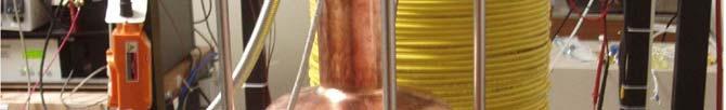
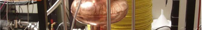
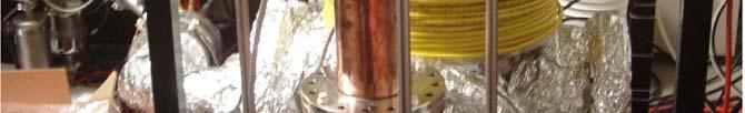
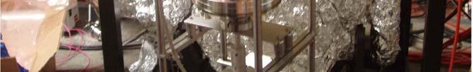
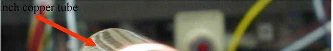
3 Coaxial Energetic Deposition TM Cathode: 60 cm conducting rod (1 cm dia). Anode: 45 cm Mo mesh tube (4.5 cm ID) Substrate: 5 cm ID minimum for this configuration Solenoid: B ranges from 0-10 mt in z + or z - direction. Note: Anode does not collect all the arc current. Mesh spacing is much larger than Debye length. Current is measured between the power supply and cathode through known resistor.
4 Magnetic field profile along z B z (mt) Solenoid 1.0 I solenoid =50A Position from Center of Solenoid (cm) Center of the anode is at the peak in B z

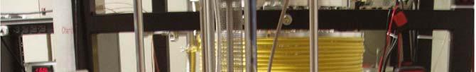
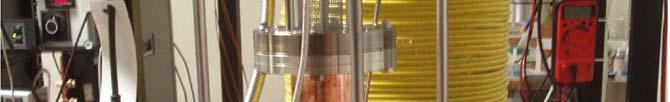
5 Coaxial Energetic DepositionTM

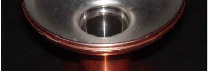
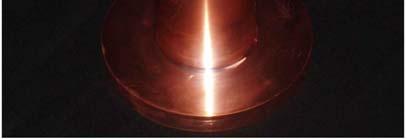
6 Rotating arc moves down the axis of a 4 φ tube

7 Cathodic Arc deposition is very different from sputtering Comparison of low energy deposition, cathodic arc deposition, and cathodic arc deposition with high voltage bias Film stress vs. incident ion energy
8 Early results revealed importance of better vacuum and higher substrate temperature on RRR Sample Effect of better vacuum on RRR Base vacuum (Torr) Ambient resistivity ( -cm) Thickness () Tc (K) RRR AASC-126-Nb AASC-126-Nb AASC-126-Nb Effect of substrate temperature on RRR
9 Nb film thickness scales linearly with total charge: erosion rate is constant y = x R 2 = Number of 200A pulses
10 RRR increases with film thickness until ~2µm
11 Latest T c & RRR results Today, vacuum is better, substrates are heated and thicker films are grown Superconducting Nb thin films with high RRR have been deposited with CED T c =9.2K and RRR=88 were measured at JLab for unfiltered film deposited on sapphire coupon T c & T c of a 0.7µm actively filtered film were measured to be 8.79K/0.46K JLab has obtained SEM, XRD and EBSD data on selected films (see talk on Thursday by Xin Zhao et al)


12 AASC-126-nb-022 analyzed by Xin Zhao (JLab) Confidence Index: 0.43

 UNS C10100")

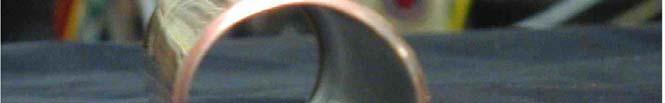
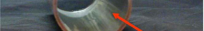
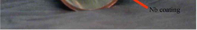
13 AASC coated Nb on Black Labs. Cu (analyzed by Xin Zhao) UNS C10100 Nb/Cu Confidence Index: 0.72 Confidence Index: 0.48
14 CED demands better Macroparticle filter CED produces micron-sized droplets of molten niobium called macro-particles along with deposition ions Macroparticles increase film roughness, limiting RF power capabilities of Nb-coated copper cavities We have demonstrated a 10x reduction in film macroparticle density using prototype coaxial filters The passive filter is inefficient: deposition rate is greatly reduced; requiring more pulses and thus producing more macroparticles that must be filtered Copper Substrate Macroparticle filter Nb Coating Nb Cathode Grounded passive filter blocks line of sight macroparticles Filter collects electrons and ions are repelled from and travel around vanes
15 Design of an active multi-particle filter Three types of active filters were tested straight vanes angled vane oriented with rotation direction angled vane oriented against rotation

16 Active Flat Macroparticle filter as designed QuickTime TIFF (LZW) de are needed to see The filter is supplied with 200A of current to create a B-field calculated to be several 100s of gauss

17 Schematic drawing of vane filter and B-field simulation
18 Throughputs of active multi-particle filters Nb film thickness was measured for the three filters Sample Description of test Thickness [nm] ratio: unfiltered/filtered # pulses thickness/pulse [nm] measurement method 7A unfiltered control profilometer B flat filter passive SEM 9A unfiltered control profilometer B flat filter active SEM CED chamber VCED-II VCED-II 12A unfiltered control profilometer VCED-I 12B angled filter orientation B passive SEM 11A unfiltered control profilometer VCED-I 11B angled filter orientation A passive SEM 14A unfiltered control profilometer VCED-I 14B angled filter orientation A active SEM 18A unfiltered control profilometer NA VCED-I 18B angled filter orientation A active profilometer 13A unfiltered control profilometer VCED-I 13B angled filter orientation B active SEM Throughput of: Flat filter passive: ~1% (poor) Flat filter active: 2.4% (better, but not acceptable) Angled filter orientation A active; 5.3% Angled filter orientation B active; 5.3% Similarity of angled filters A and B proves that ion flight time through filter is «plasma dwell time in vane

")


19 Macro-particle distributions measured with ImageJ software Unfiltered CED film on Si substrate at 200x (Nb-005) Start with unfiltered microscope image of CED deposited coupon Do some digital filtering to improve contrast and develop histogram using ImageJ

20 Particle distributions for active and passive flat filters Macro-particle distributions for passive and active flat filter Debris is reduced, but throughput is unacceptably low
21 Passive vane filter A has no effect on debris! Macro-particle distributions for passive vane filter vs. no filter Could vanes themselves be a source of debris? (is the treatment worse than the disease?)


22 Active vane filter B is better, but.. Macro-particle distributions for active vane filters Need RF tests to establish acceptable macro-particle distribution thresholds

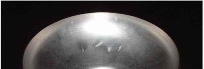
23 Cross section SEM image of film 14B This local SEM shows a rather smooth surface after active filtering
24 Hall plasma model for active multi-particle filter Ion momentum eq. r Electron fluid with drift speed ν Which leads to: deflection: Importance of Hall term: Alfven speed scaling: NM d r V dt p e + Ne( r E + = r Jx r B / c ( p e + p i ) r vx r B c ) + Nm τ (r v r V ) = 0 J y = ωτ J r e ( yx ) b ) ) r Jx r d B δv dt 2JBd ρc ρcv 0 θ 1 5 d jbd ρv 0 2 j y = ωτ j n θ 1 5 I arc B NvLρV 0 2 ωτ 1 2π V A 2 = B arc B /4πρ B arc B NvρV ωτ 2 0 θ 2 Nv V A 2 V 0 2 ωτ
25 Measured film thickness enables an estimate of plasma density measured film thickness/pulse= nm average substrate= 6.95E-08 g/cm 2 bulk Nb density anode screen transparency= 0.56 average cathode surface= 1.21E-06 g/cm 2 conserve flux cathode conduction area= 182 cm 2 eroded mass/pulse= 2.20E-04 g flux*area average current= 150 A pulse width= s average erosion rate= 2.0E-05 g/c eroded mass/charge "dwell" time in vane= 4.03E-03 s instantaneous 2.95E-06 g/cm 2 fluence@vane= 7.32E-04 g/cm 2 -s ion speed= 1.00E+06 cm/s electron density in vane= 1.92E+13 cm -3 "spoke" flux -50eV ions
26 Design of an active multi-particle filter d = Lcosα, so that the line of sight along z is completely blocked assume that every particle undergoes an impulsive deflection through a unique angle θ = π/2 - φ on the midline connecting the vanes. Observe that for α = 30 degrees half the incident particles, (those incident with x < d/2), will not reach the midline. Thus the efficiency for transmission can be no greater than fifty percent Only particles entering the filter at x > x 1 will pass through the filter Define the transmission efficiency E by: E = 1 x 1 /d leads to: E = 0.5(tanα)cotφ =0.5(tanα)tanθ θ = B arc Bωτ/(2πN v ρv 02 ) (using V θ ) Nv V ωτ A = B arc B /4πρ 0 Observe that vane filter efficiency (throughput) scales as B 3 (the third factor comes from the Hall parameter): In PhII we will use auxiliary current to vanes V A 2
27 Advanced vane filter concepts QuickTime and a TIFF (LZW) decompressor are needed to see this picture. Two-stage deflection design Three-stage deflection design Plasma physics model provides guidance to higher efficiency vane filter designs that should also reduce filter generated debris
28 Increase process repetition rate through hardware/software modification Reducing deposition chamber base pressure below current 5x10⁻⁹ Torr is impractical 1.0E E+04 Operating regime 0.25 Hz operation 2.0 Hz operation Increasing repetition rate allows increased flux of deposition ions at film surface relative to background contaminants: thus film purity is increased 1.0E E E+01 Superconducting properties are greatly affected by film purity 1.0E+00 High RRR 1.0E E E E E E-07 Oxygen Partial Pressure (Torr) To increase the repetition rate, 400A IGBT switches are being installed to control the arc s turn on and turn off Initial switch testing is promising but more experiments are required to optimize switch controls. Higher repetition rate to ~2 Hz should reduce impurities by 10x
29 Future plans Make further improvements to active filters using design parameters developed in Phase I Obtain RF data on coupons to improve specifications on acceptable macro-particle distributions Increase discharge duty factor to further reduce O 2 contamination and increase RRR for smoother, actively filtered films Coat Cu RF cavities and have them tested at JLab
Niobium Coating of Copper Cavities by UHV Cathodic Arc: progress report
 Niobium Coating of Copper Cavities by UHV Cathodic Arc: progress report L. Catani, A. Cianchi, D. Digiovenale, J. Lorkiewicz, Prof. S. Tazzari, INFN-Roma "Tor Vergata", Italy Roberto Russo, Istituto di
UHV ARC DEPOSITION FOR RF SUPERCONDUCTING CAVITY
 UHV ARC DEPOSITION FOR RF SUPERCONDUCTING CAVITY S. Tazzari, A. Cianchi, R. Russo, University of Rome Tor Vergata and INFN-Roma2, Rome, Italy L. Catani, INFN-Roma2, Rome, Italy F. Tazzioli, Laboratori
Partial Replication of Storms/Scanlan Glow Discharge Radiation
 Partial Replication of Storms/Scanlan Glow Discharge Radiation Rick Cantwell and Matt McConnell Coolescence, LLC March 2008 Introduction The Storms/Scanlan paper 1 presented at the 8 th international workshop
A DC POST-MAGNETRON CONFIGURATION FOR NIOBIUM SPUTTERING INTO 1.5 GHz COPPER MONOCELLS.
 A DC POST-MAGNETRON CONFIGURATION FOR NIOBIUM SPUTTERING INTO 1.5 GHz COPPER MONOCELLS. V. PALMIERI, R. PRECISO, V.L. RUZINOV A, S.Yu. STARK A ISTITUTO NAZIONALE DI FISICA NUCLEARE Laboratori Nazionali
Schematic diagram of the DAP
 Outline Introduction Transmission mode measurement results Previous emission measurement Trapping mechanics Emission measurement with new circuits Emission images Future plan and conclusion Schematic diagram
Progress towards Actinic Patterned Mask Inspection. Oleg Khodykin
 Progress towards Actinic Patterned Mask Inspection Oleg Khodykin Outline Status (technical) of EUV Actinic Reticle Inspection program Xe based LPP source as bright and reliable solution Requirements Choice
Zpulser LLC. Industry Proven HIPIMS/HPPMS Plasma Generators Based on MPP Technology.
 Zpulser LLC Industry Proven HIPIMS/HPPMS Plasma Generators Based on MPP Technology. Zond/ Zpulser Zpulser is the sales/manufacturing division of Zond Inc. We manufacture unique pulsed dc generators for
Gencoa 3G Circular Magnetron
 Gencoa 3G Circular Magnetron Presenting Gencoa s 3 rd generation range of circular magnetrons November 2017 www.gencoa.com 1 Contents Product Overview Introduction 3G Design Features 3G Mechanical Options
High Power Pulse Plasma Generators (HPPMS/HIPIMS/MPP) for Material Processing Applications. Zond, Inc / Zpulser, LLC. Mansfield, MA USA
 for Material Processing Applications. Zond, Inc / Zpulser, LLC. Mansfield, MA USA") High Power Pulse Plasma Generators (HPPMS/HIPIMS/MPP) for Material Processing Applications. Zond, Inc / Zpulser, LLC. Mansfield, MA 02048 USA Magnetron Sputtering Magnetron sputtering is a widely used
High Power Pulse Plasma Generators (HPPMS/HIPIMS/MPP) for Material Processing Applications. Zond, Inc / Zpulser, LLC. Mansfield, MA 02048 USA Magnetron Sputtering Magnetron sputtering is a widely used
WG4 summary talk ~Performance frontier~
 WG4 summary talk ~Performance frontier~ 2016/7/8 TTC meeting @ Saclay WG4 S. Aull, A. Grassellino, K.Umemori WG3 S. Belomestnykh, J. Hao, E. Jensen (Joint session for High gradient and High-Q) Thin film
ICRF-Edge and Surface Interactions
 ICRF-Edge and Surface Interactions D. A. D Ippolito and J. R. Myra Lodestar Research Corporation Presented at the 19 th PSI Meeting, San Diego, CA, May 24-28, 2009 Introduction Heating and current drive
SOLVIX ARC AND BIAS SERIES
 CATHODIC ARC DEPOSITION WITH PRECISE PROCESS CONTROL AND SUPERIOR FILM QUALITY Arc Units 60, 100, 210, and 400 A Bias Units 3 to 30 kw Regulation Modes Current, power, and voltage 2018 Advanced Energy
Nb 3 Sn Present Status and Potential as an Alternative SRF Material. S. Posen and M. Liepe, Cornell University
 Nb 3 Sn Present Status and Potential as an Alternative SRF Material S. Posen and M. Liepe, Cornell University LINAC 2014 Geneva, Switzerland September 2, 2014 Limits of Modern SRF Technology Low DF, high
UPDATE ON THE R&D OF VERTICAL BUFFERED ELECTROPOLISHING ON NIOBIUM SAMPLES AND SRF SINGLE CELL CAVITIES*
 UPDATE ON THE R&D OF VERTICAL BUFFERED ELECTROPOLISHING ON NIOBIUM SAMPLES AND SRF SINGLE CELL CAVITIES* A.T. Wu 1, S. Jin 1,2, X.Y Lu 2, R.A. Rimmer 1, K. Zhao 2, L. Lin 2, and J. Mammosser 1 1 Institute
ANALYTICAL MICRO X-RAY FLUORESCENCE SPECTROMETER
 Copyright(c)JCPDS-International Centre for Diffraction Data 2001,Advances in X-ray Analysis,Vol.44 325 ANALYTICAL MICRO X-RAY FLUORESCENCE SPECTROMETER ABSTRACT William Chang, Jonathan Kerner, and Edward
Measuring the Ion Current to the Substrate During Deposition of Thin Films by Hollow Cathode Plasma Jet
 WDS'07 Proceedings of Contributed Papers, Part II, 212 217, 2007. ISBN 978-80-7378-024-1 MATFYZPRESS Measuring the Ion Current to the Substrate During Deposition of Thin Films by Hollow Cathode Plasma
Flux Gate Magnetometry Applied to RF Cavities
 Flux Gate Magnetometry Applied to RF Cavities Carmela Bonavolontà Department of Materials and Production Engineering, University of Naples Federico II,Italy Istituto Nazionale Fisica Nucleare, Legnaro
Laser-Produced Sn-plasma for Highvolume Manufacturing EUV Lithography
 Panel discussion Laser-Produced Sn-plasma for Highvolume Manufacturing EUV Lithography Akira Endo * Extreme Ultraviolet Lithography System Development Association Gigaphoton Inc * 2008 EUVL Workshop 11
EUV Light Source The Path to HVM Scalability in Practice
 EUV Light Source The Path to HVM Scalability in Practice Harald Verbraak et al. (all people at XTREME) 2011 International Workshop on EUV and Soft X-ray Sources Nov. 2011 Today s Talk o LDP Technology
A novel sputtering technique: Inductively Coupled Impulse Sputtering (ICIS)
") A novel sputtering technique: Inductively Coupled Impulse Sputtering (ICIS) LOCH, Daniel and EHIASARIAN, Arutiun Available
A novel sputtering technique: Inductively Coupled Impulse Sputtering (ICIS) LOCH, Daniel and EHIASARIAN, Arutiun Available
Magnetic and Electromagnetic Microsystems. 4. Example: magnetic read/write head
 Magnetic and Electromagnetic Microsystems 1. Magnetic Sensors 2. Magnetic Actuators 3. Electromagnetic Sensors 4. Example: magnetic read/write head (C) Andrei Sazonov 2005, 2006 1 Magnetic microsystems
Nano-structured superconducting single-photon detector
 Nano-structured superconducting single-photon detector G. Gol'tsman *a, A. Korneev a,v. Izbenko a, K. Smirnov a, P. Kouminov a, B. Voronov a, A. Verevkin b, J. Zhang b, A. Pearlman b, W. Slysz b, and R.
High Power Couplers for TTF - FEL
 High Power Couplers for TTF - FEL 1. Requirements for High Power Couplers on superconducting Cavities 2. Characteristics of pulsed couplers 3. Standing wave pattern in the coaxial coupler line 4. Advantages
State-of-the-art thin film X-ray optics for synchrotrons and FEL sources. Frank Hertlein Incoatec GmbH Geesthacht, Germany
 State-of-the-art thin film X-ray optics for synchrotrons and FEL sources Frank Hertlein Incoatec GmbH Geesthacht, Germany Incoatec: Innovative Coating Technologies Incoatec is founded with Bruker AXS in
EXPERIMENT # 3: Oxidation and Etching Tuesday 2/3/98 and 2/5/98 Thursday 2/10/98 and 2/12/98
 EXPERIMENT # 3: Oxidation and Etching Tuesday 2/3/98 and 2/5/98 Thursday 2/10/98 and 2/12/98 Experiment # 3: Oxidation of silicon - Oxide etching and Resist stripping Measurement of oxide thickness using
Amit Roy Director, IUAC
 SUPERCONDUCTING RF DEVELOPMENT AT INTER-UNIVERSITY ACCELERATOR CENTRE (IUAC) (JOINT PROPOSAL FROM IUAC & Delhi University (DU)) Amit Roy Director, IUAC to be presented by Kirti Ranjan (DU / Fermilab) Overview
C-Mod ICRF Research Program
 C-Mod ICRF Research Program C-Mod Ideas Forum December 2-6, 2004 MIT PSFC Presented by Steve Wukitch Outline: 1. Overview of ICRF program 2. Summary of MP s and proposals ICRF Highlights Antenna Performance
Room-Temperature-Processed Flexible Amorphous InGaZnO Thin Film Transistor
 Supporting Information Room-Temperature-Processed Flexible Amorphous InGaZnO Thin Film Transistor Xiang Xiao 1, Letao Zhang 1, Yang Shao 1, Xiaoliang Zhou 2, Hongyu He 1, and Shengdong Zhang 1,2 * 1 School
Proceedings of the Fourth Workshop on RF Superconductivity, KEK, Tsukuba, Japan
 ACTVTES ON RF SUPERCONDUCTVTY N FRASCAT, GENOVA, MLAN0 LABORATORES R. Boni, A. Cattoni, A. Gallo, U. Gambardella, D. Di Gioacchino, G. Modestino, C. Pagani*, R. Parodi**, L. Serafini*, B. Spataro, F. Tazzioli,
QWR Nb sputtering. Anna Maria Porcellato. MoP04. S. Stark, F. Stivanello, V. Palmieri INFN Laboratori Nazionali di Legnaro
 QWR Nb sputtering MoP04 Anna Maria Porcellato S. Stark, F. Stivanello, V. Palmieri INFN Laboratori Nazionali di Legnaro 12 International Workshop on RF Superconductivity, Ithaca, 08-15/07/2005 SC Quarter
Microtools Shaped by Focused Ion Beam Milling and the Fabrication of Cylindrical Coils
 Microtools Shaped by Focused Ion Beam Milling and the Fabrication of Cylindrical Coils M.J. Vasile, D.P. Adams #, and Y.N. Picard* Sandia National Laboratories P.O. Box 5800, MS 0959 Albuquerque, NM, 87185
Tutorial: designing a converging-beam electron gun and focusing solenoid with Trak and PerMag
 Tutorial: designing a converging-beam electron gun and focusing solenoid with Trak and PerMag Stanley Humphries, Copyright 2012 Field Precision PO Box 13595, Albuquerque, NM 87192 U.S.A. Telephone: +1-505-220-3975
Construction Status of SuperKEKB Vacuum System
 Construction Status of SuperKEKB Vacuum System Mt. Tsukuba SuperKEKB ( 3000 m) Damping Ring Linac KEK Tsukuba site Fourth Workshop on the Operation of Large Vacuum systems (OLAV IV) April 2, 2014 Kyo Shibata
POLYMER MICROSTRUCTURE WITH TILTED MICROPILLAR ARRAY AND METHOD OF FABRICATING THE SAME
 POLYMER MICROSTRUCTURE WITH TILTED MICROPILLAR ARRAY AND METHOD OF FABRICATING THE SAME Field of the Invention The present invention relates to a polymer microstructure. In particular, the present invention
Japan Update. EUVA (Extreme Ultraviolet Lithography System Development Association) Koichi Toyoda. SOURCE TWG 2 March, 2005 San Jose
 Koichi Toyoda. SOURCE TWG 2 March, 2005 San Jose") 1 Japan Update EUVA (Extreme Ultraviolet Lithography System Development Association) Koichi Toyoda SOURCE TWG 2 March, 2005 San Jose Outline 2 EUVA LPP at Hiratsuka R&D Center GDPP at Gotenba Branch Lab.
1 Japan Update EUVA (Extreme Ultraviolet Lithography System Development Association) Koichi Toyoda SOURCE TWG 2 March, 2005 San Jose Outline 2 EUVA LPP at Hiratsuka R&D Center GDPP at Gotenba Branch Lab.
Rapid and inexpensive fabrication of polymeric microfluidic devices via toner transfer masking
 Easley et al. Toner Transfer Masking Page -1- B816575K_supplementary_revd.doc December 3, 2008 Supplementary Information for Rapid and inexpensive fabrication of polymeric microfluidic devices via toner
DOE/ET PFC/RR-87-10
 PFC/RR-87-10 DOE/ET-51013-227 Concepts of Millimeter/Submillimeter Wave Cavities, Mode Converters and Waveguides Using High Temperature Superconducting Material D.R Chon; L. Bromberg; W. Halverson* B.
State-of-The-Art Dielectric Etch Technology
 State-of-The-Art Dielectric Etch Technology Koichi Yatsuda Product Marketing Manager Etch System Business Unit November 5 th, 2010 TM Outline Dielectric Etch Challenges for State-of-The-Art Devices Control
LOW-β SC RF CAVITY INVESTIGATIONS
 LOW-β SC RF CAVITY INVESTIGATIONS E. Zaplatin, W. Braeutigam, R. Stassen, FZJ, Juelich, Germany Abstract At present, many accelerators favour the use of SC cavities as accelerating RF structures. For some
Micro-sensors - what happens when you make "classical" devices "small": MEMS devices and integrated bolometric IR detectors
 Micro-sensors - what happens when you make "classical" devices "small": MEMS devices and integrated bolometric IR detectors Dean P. Neikirk 1 MURI bio-ir sensors kick-off 6/16/98 Where are the targets
MULTIPACTING IN THE CRAB CAVITY
 MULTIPACTING IN TH CRAB CAVITY Y. Morita, K. Hara, K. Hosoyama, A. Kabe, Y. Kojima, H. Nakai, KK, 1-1, Oho, Tsukuba, Ibaraki 3-81, JAPAN Md. M. Rahman, K. Nakanishi, Graduate University for Advanced Studies,
Today s Outline - January 25, C. Segre (IIT) PHYS Spring 2018 January 25, / 26
 PHYS Spring 2018 January 25, / 26") Today s Outline - January 25, 2018 C. Segre (IIT) PHYS 570 - Spring 2018 January 25, 2018 1 / 26 Today s Outline - January 25, 2018 HW #2 C. Segre (IIT) PHYS 570 - Spring 2018 January 25, 2018 1 / 26 Today
Today s Outline - January 25, 2018 C. Segre (IIT) PHYS 570 - Spring 2018 January 25, 2018 1 / 26 Today s Outline - January 25, 2018 HW #2 C. Segre (IIT) PHYS 570 - Spring 2018 January 25, 2018 1 / 26 Today
A scanning tunneling microscopy based potentiometry technique and its application to the local sensing of the spin Hall effect
 A scanning tunneling microscopy based potentiometry technique and its application to the local sensing of the spin Hall effect Ting Xie 1, a), Michael Dreyer 2, David Bowen 3, Dan Hinkel 3, R. E. Butera
Machine-Aligned Fabrication of Submicron SIS Tunnel Junctions Using a Focused Ion Beam
 Machine-Aligned Fabrication of Submicron SIS Tunnel Junctions Using a Focused Ion Beam Robert. B. Bass, Jian. Z. Zhang and Aurthur. W. Lichtenberger Department of Electrical Engineering, University of
arxiv: v1 [cond-mat.supr-con] 21 Oct 2011
![arxiv: v1 [cond-mat.supr-con] 21 Oct 2011](/thumbs/93/118044439.jpg "arxiv: v1 [cond-mat.supr-con] 21 Oct 2011") Journal of Low Temperature Physics manuscript No. (will be inserted by the editor) arxiv:1110.4839v1 [cond-mat.supr-con] 21 Oct 2011 Peter J. Lowell Galen C. O Neil Jason M. Underwood Joel N. Ullom Andreev
Journal of Low Temperature Physics manuscript No. (will be inserted by the editor) arxiv:1110.4839v1 [cond-mat.supr-con] 21 Oct 2011 Peter J. Lowell Galen C. O Neil Jason M. Underwood Joel N. Ullom Andreev
Advanced Arc-Handling for HiPIMS-PS
 Advanced Arc-Handling for HiPIMS-PS Advanced ARC-Handling for HiPIMS-PS Gerhard Eichenhofer April 22, 2013 SVC TechCon 2013 is now Advanced Arc-Handling for HiPIMS-PS Advanced ARC-Handling for HiPIMS-PS
Resonant Cavity Hollow Cathode Progress
 Resonant Cavity Hollow Cathode Progress IEPC-25-7 Presented at the 29 th International Electric Propulsion Conference, Princeton University, October 31 November 4, 25 Kevin D. Diamant The Aerospace Corporation,
Magnesium and Magnesium-Silicide coated Silicon Nanowire composite Anodes for. Lithium-ion Batteries
 Magnesium and Magnesium-Silicide coated Silicon Nanowire composite Anodes for Lithium-ion Batteries Alireza Kohandehghan a,b, Peter Kalisvaart a,b,*, Martin Kupsta b, Beniamin Zahiri a,b, Babak Shalchi
CENTRIFUGAL BARREL POLISHING OF CAVITIES WORLDWIDE
 CENTRIFUGAL BARREL POLISHING OF CAVITIES WORLDWIDE C. Cooper #, Fermi National Accelerator Laboratory, Batavia, IL, U.S.A. Kenji Saito, KEK, High Energy Accelerator Research Organization, Tsukuba, Japan
DQW HOM Coupler for LHC
 DQW HOM Coupler for LHC J. A. Mitchell 1, 2 1 Engineering Department Lancaster University 2 BE-RF-BR Section CERN 03/07/2017 J. A. Mitchell (PhD Student) HL LHC UK Jul 17 03/07/2017 1 / 27 Outline 1 LHC
HIGH POWER COUPLER FOR THE TESLA TEST FACILITY
 Abstract HIGH POWER COUPLER FOR THE TESLA TEST FACILITY W.-D. Moeller * for the TESLA Collaboration, Deutsches Elektronen-Synchrotron DESY, D-22603 Hamburg, Germany The TeV Energy Superconducting Linear
SQUID Test Structures Presented by Makoto Ishikawa
 SQUID Test Structures Presented by Makoto Ishikawa We need to optimize the microfabrication process for making an SIS tunnel junction because it is such an important structure in a SQUID. Figure 1 is a
Microscopic Examination and Elemental Analysis of Surface Defects in LEP Superconducting Cavities
 Microscopic Examination and Elemental nalysis of Surface Defects in LEP Superconducting Cavities C. Benvenuti, R. Cosso, M. Hauer, N. Hellgren, D. Lacarrere CERN, 1211 Geneva 23, Switzerland bstract diagnostic
CLUSTERLINE RAD VERSATILE DYNAMIC SPUTTER SYSTEM OPTOELECTRONICS, MEMS, PHOTONICS, WIRELESS
 CLUSTERLINE RAD VERSATILE DYNAMIC SPUTTER SYSTEM OPTOELECTRONICS, MEMS, PHOTONICS, WIRELESS CLUSTERLINE RAD Enabling your roadmap in thin film deposition The combination of Evatec s process know-how and
4H-SiC V-Groove Trench MOSFETs with the Buried p + Regions
 ELECTRONICS 4H-SiC V-Groove Trench MOSFETs with the Buried p + Regions Yu SAITOH*, Toru HIYOSHI, Keiji WADA, Takeyoshi MASUDA, Takashi TSUNO and Yasuki MIKAMURA ----------------------------------------------------------------------------------------------------------------------------------------------------------------------------------------------------------------------------------------------------------
X-rays. X-rays are produced when electrons are accelerated and collide with a target. X-rays are sometimes characterized by the generating voltage
 X-rays Ouch! 1 X-rays X-rays are produced when electrons are accelerated and collide with a target Bremsstrahlung x-rays Characteristic x-rays X-rays are sometimes characterized by the generating voltage
MicroVacuum Arc Thruster Design for a CubeSat Class Satellite
 MicroVacuum Arc Thruster Design for a CubeSat Class Satellite SSC02-I-2 and John William Hartmann University of Illinois in Urbana and Champaign, 306 Talbot Lab, 104 S Wright St., Urbana IL 61802, (217)
SUPPLEMENTARY INFORMATION
 Room-temperature continuous-wave electrically injected InGaN-based laser directly grown on Si Authors: Yi Sun 1,2, Kun Zhou 1, Qian Sun 1 *, Jianping Liu 1, Meixin Feng 1, Zengcheng Li 1, Yu Zhou 1, Liqun
Initial Results from the C-Mod Prototype Polarimeter/Interferometer
 Initial Results from the C-Mod Prototype Polarimeter/Interferometer K. R. Smith, J. Irby, R. Leccacorvi, E. Marmar, R. Murray, R. Vieira October 24-28, 2005 APS-DPP Conference 1 Abstract An FIR interferometer-polarimeter
Plasma Enhanced Chemical Vapor Deposition (PECVD) of Silicon Nitride (SiNx) Using Oxford Instruments System 100 PECVD
 of Silicon Nitride (SiNx) Using Oxford Instruments System 100 PECVD") University of Pennsylvania ScholarlyCommons Tool Data Browse by Type 2-28-2017 Plasma Enhanced Chemical Vapor Deposition (PECVD) of Silicon Nitride (SiNx) Using Oxford Instruments System 100 PECVD Meredith
University of Pennsylvania ScholarlyCommons Tool Data Browse by Type 2-28-2017 Plasma Enhanced Chemical Vapor Deposition (PECVD) of Silicon Nitride (SiNx) Using Oxford Instruments System 100 PECVD Meredith
Importance of edge physics in optimizing ICRF performance
 Importance of edge physics in optimizing ICRF performance D. A. D'Ippolito and J. R. Myra Research Corp., Boulder, CO Acknowledgements D. A. Russell, M. D. Carter, RF SciDAC Team Presented at the ECC Workshop
Sustainment and Additional Heating of High-Beta Field-Reversed Configuration Plasmas
 1 Sustainment and Additional Heating of High-Beta Field-Reversed Configuration Plasmas S. Okada, T. Fukuda, K. Kitano, H. Sumikura, T. Higashikozono, M. Inomoto, S. Yoshimura, M. Ohta and S. Goto Science
Physics Laboratory Scattering of Photons from Electrons: Compton Scattering
 RR Oct 2001 SS Dec 2001 MJ Oct 2009 Physics 34000 Laboratory Scattering of Photons from Electrons: Compton Scattering Objective: To measure the energy of high energy photons scattered from electrons in
Field Emission Cathodes using Carbon Nanotubes
 21st Microelectronics Workshop, Tsukuba, Japan, October 2008 Field Emission Cathodes using Carbon Nanotubes by Yasushi Ohkawa, Koji Matsumoto, and Shoji Kitamura Innovative Technology Research Center,
MuCool Test Area Experimental Program Summary
 MuCool Test Area Experimental Program Summary Alexey Kochemirovskiy The University of Chicago/Fermilab Alexey Kochemirovskiy NuFact'16 (Quy Nhon, August 21-27, 2016) Outline Introduction Motivation MTA
Lecture 20: Optical Tools for MEMS Imaging
 MECH 466 Microelectromechanical Systems University of Victoria Dept. of Mechanical Engineering Lecture 20: Optical Tools for MEMS Imaging 1 Overview Optical Microscopes Video Microscopes Scanning Electron
HIGH POWER INPUT COUPLERS FOR THE STF BASELINE CAVITY SYSTEM AT KEK
 HIGH POWER INPUT COUPLERS FOR THE STF BASELINE CAVITY SYSTEM AT KEK E. Kako #, H. Hayano, S. Noguchi, T. Shishido, K. Watanabe and Y. Yamamoto KEK, Tsukuba, Ibaraki, 305-0801, Japan Abstract An input coupler,
Gyroklystron Research at CCR
 Gyroklystron Research at CCR RLI@calcreek.com Lawrence Ives, Michael Read, Jeff Neilson, Philipp Borchard and Max Mizuhara Calabazas Creek Research, Inc. 20937 Comer Drive, Saratoga, CA 95070-3753 W. Lawson
EXPERIMENT # 3: Oxidation and Etching Week of 1/31/05 and 2/7/05
 EXPERIMENT # 3: Oxidation and Etching Week of 1/31/05 and 2/7/05 Experiment # 3: Oxidation of silicon - Oxide etching and Resist stripping Measurement of oxide thickness using different methods The purpose
A proposal for the measurement of the non-stationary Casimir effect
 A proposal for the measurement of the non-stationary Casimir effect Giuseppe Ruoso INFN - Laboratori Nazionali di Legnaro - aim of the experiment - mechanical and effective motion - experimental set-up
Thermionic Bunched Electron Sources for High-Energy Electron Cooling
 Thermionic Bunched Electron Sources for High-Energy Electron Cooling Vadim Jabotinski 1, Yaroslav Derbenev 2, and Philippe Piot 3 1 Institute for Physics and Technology (Alexandria, VA) 2 Thomas Jefferson
Helicon mode formation and rf power deposition in a helicon source
 Helicon mode formation and rf power deposition in a helicon source Michael Krämer & Kari Niemi Institut für Experimentalphysik II, Ruhr-Universität D-4478 Bochum, Germany Helicon Mini-Conference APS-DPP,
The TESLA Linear Collider. Winfried Decking (DESY) for the TESLA Collaboration
 for the TESLA Collaboration") The TESLA Linear Collider Winfried Decking (DESY) for the TESLA Collaboration Outline Project Overview Highlights 2000/2001 Publication of the TDR Cavity R&D TTF Operation A0 and PITZ TESLA Beam Dynamics
The TESLA Linear Collider Winfried Decking (DESY) for the TESLA Collaboration Outline Project Overview Highlights 2000/2001 Publication of the TDR Cavity R&D TTF Operation A0 and PITZ TESLA Beam Dynamics
Third Harmonic Superconducting passive cavities in ELETTRA and SLS
 RF superconductivity application to synchrotron radiation light sources Third Harmonic Superconducting passive cavities in ELETTRA and SLS 2 cryomodules (one per machine) with 2 Nb/Cu cavities at 1.5 GHz
Radiation Detection Instrumentation
 Radiation Detection Instrumentation Principles of Detection and Gas-filled Ionization Chambers Neutron Sensitive Ionization Chambers Detection of radiation is a consequence of radiation interaction with
Cavity development for TESLA
 Cavity development for TESLA Lutz.Lilje@desy.de DESY -FDET- Cavity basics History: Limitations and solutions»material inclusions»weld defects»field emission»increased surface resistance at high field Performance
A 94 GHz Overmoded Traveling Wave Tube (TWT) Amplifier
 Amplifier") 1 A 94 GHz Overmoded Traveling Wave Tube (TWT) Amplifier Elizabeth J. Kowalski MIT Plasma Science and Fusion Center MURI Teleseminar December 5, 2014 2 Outline Introduction TWT Design and Cold Tests TWT
1 A 94 GHz Overmoded Traveling Wave Tube (TWT) Amplifier Elizabeth J. Kowalski MIT Plasma Science and Fusion Center MURI Teleseminar December 5, 2014 2 Outline Introduction TWT Design and Cold Tests TWT
THE PROTOTYPE FUNDAMENTAL POWER COUPLER FOR THE SPALLATION NEUTRON SOURCE SUPERCONDUCTING CAVITIES: DESIGN AND INITIAL TEST RESULTS*
 THE PROTOTYPE FUNDAMENTAL POWER COUPLER FOR THE SPALLATION NEUTRON SOURCE SUPERCONDUCTING CAVITIES: DESIGN AND INITIAL TEST RESULTS* K. M. Wilson,I.E.Campisi,E.F.Daly,G.K.Davis,M.Drury,J.E.Henry,P.Kneisel,G.
RECENT DEVELOPMENTS IN ELECTROPOLISHING AND TUMBLING R&D AT FERMILAB
 FERMILAB-CONF-09-539-AD-TD RECENT DEVELOPMENTS IN ELECTROPOLISHING AND TUMBLING R&D AT FERMILAB C. Cooper #, J. Brandt, L. Cooley, M. Ge, E. Harms, T. Khabiboulline, J. Ozelis, Fermilab, Batavia, IL.,
RF thermal and new cold part design studies on TTF-III input coupler for Project-X
 RF thermal and new cold part design studies on TTF-III input coupler for Project-X PEI Shilun( 裴士伦 ) 1; 1) Chris E Adolphsen 2 LI Zenghai( 李增海 ) 2 Nikolay A Solyak 3 Ivan V Gonin 3 1 Institute of High
CMP for More Than Moore
 2009 Levitronix Conference on CMP Gerfried Zwicker Fraunhofer Institute for Silicon Technology ISIT Itzehoe, Germany gerfried.zwicker@isit.fraunhofer.de Contents Moore s Law and More Than Moore Comparison:
A flexible HiPIMS pulser for the latest generation of coatings
 HIPSTER 1 Pulser A flexible HiPIMS pulser for the latest generation of coatings Reactive mode HiPSTER 1 HiPIMS Pulser Our HiPSTER HiPIMS units are designed by experts in the field with an excellent track
Development of a charged-particle accumulator using an RF confinement method FA
 Development of a charged-particle accumulator using an RF confinement method FA4869-08-1-4075 Ryugo S. Hayano, University of Tokyo 1 Impact of the LHC accident This project, development of a charged-particle
Launcher Study for KSTAR 5 GHz LHCD System*
 Launcher Study for KSTAR 5 GHz LHCD System* Joint Workshop on RF Heating and Current Drive in Fusion Plasmas October 24, 2005 Pohang Accelerator Laboratory, Pohang Y. S. Bae, M. H. Cho, W. Namkung Department
Control of Sputter Process for Improved Run-to-run Repeatability
 Control of Sputter Process for Improved Run-to-run Repeatability S. Ghosal, R.L. Kosut, J.L. Ebert, L. Porter SC Solutions, Santa Clara, CA 95054 E-mail ghosal@scsolutions.com D. Brownell, D. Wang Nonvolatile
XRF Instrumentation. Introduction to spectrometer
 XRF Instrumentation Introduction to spectrometer AMPTEK, INC., Bedford, MA 01730 Ph: +1 781 275 2242 Fax: +1 781 275 3470 sales@amptek.com 1 Instrument Excitation source Sample X-ray tube or radioisotope
Measurement of Microscopic Three-dimensional Profiles with High Accuracy and Simple Operation
 238 Hitachi Review Vol. 65 (2016), No. 7 Featured Articles Measurement of Microscopic Three-dimensional Profiles with High Accuracy and Simple Operation AFM5500M Scanning Probe Microscope Satoshi Hasumura
Dosimetry and Position Sensing Ionization Chamber for Ion Beam Tracking
 Features Dosimetry and Position Sensing Ionization Chamber for Ion Beam Tracking 25 cm x 25 cm sensitive area Ionization chamber with integral plane readout for dosimetry and 128 by 128 strip readout for
Plasma Confinement by Pressure of Rotating Magnetic Field in Toroidal Device
 1 ICC/P5-41 Plasma Confinement by Pressure of Rotating Magnetic Field in Toroidal Device V. Svidzinski 1 1 FAR-TECH, Inc., San Diego, USA Corresponding Author: svidzinski@far-tech.com Abstract: Plasma
System Upgrades to the DIII-D Facility
 System Upgrades to the DIII-D Facility A.G. Kellman for the DIII-D Team 24th Symposium on Fusion Technology Warsaw, Poland September 11-15, 2006 Upgrades Performed During the Long Torus Opening (LTOA)
Profile Scan Studies on the Levitated Dipole Experiment
 Profile Scan Studies on the Levitated Dipole Experiment Columbia University A.K. Hansen, D.T. Garnier, M.E. Mauel, E.E. Ortiz Columbia University J. Kesner, A.C. Boxer, J.E. Ellsworth, I. Karim, S. Mahar,
MICROWAVE HALL THRUSTER DEVELOPMENT
 MICROWAVE HALL THRUSTER DEVELOPMENT 1 Pedro MOLINA-MORALES, Hitoshi KUNINAKA, Kyoichiro TOKI Institute of Space and Astronautical Science (ISAS) 3-1-1 Yoshinodai, Sagamihara, Kanagawa, 229-851, Japan Yoshihiro
3D modeling of toroidal asymmetry due to localized divertor nitrogen puffing on Alcator C-Mod
 3D modeling of toroidal asymmetry due to localized divertor nitrogen puffing on Alcator C-Mod J.D. Lore 1, M.L. Reinke 2, B. LaBombard 2, B. Lipschultz 3, R. Pitts 4 1 Oak Ridge National Laboratory, Oak
Commissioning of the ALICE SRF Systems at Daresbury Laboratory Alan Wheelhouse, ASTeC, STFC Daresbury Laboratory ESLS RF 1 st 2 nd October 2008
 Commissioning of the ALICE SRF Systems at Daresbury Laboratory Alan Wheelhouse, ASTeC, STFC Daresbury Laboratory ESLS RF 1 st 2 nd October 2008 Overview ALICE (Accelerators and Lasers In Combined Experiments)
High acceleration gradient. Critical applications: Linear colliders e.g. ILC X-ray FELs e.g. DESY XFEL
 High acceleration gradient Critical applications: Linear colliders e.g. ILC X-ray FELs e.g. DESY XFEL Critical points The physical limitation of a SC resonator is given by the requirement that the RF magnetic
knowledge generating HIPIMS NEW POSSIBILITIES FOR INDUSTRY Background TRUMPF Hüttinger White Paper 04/2017
 generating knowledge HIPIMS NEW POSSIBILITIES FOR INDUSTRY Figure 1: Schematic representation of the HIPIMS technology compared to DC and Pulsed-DC sputtering. In HIPIMS the same average power is delivered
Study on Glow Discharge Plasma Used in Polyester. surface modification
 Study on Glow Discharge Plasma Used in Polyester Surface Modification LIU Wenzheng ( ), LEI Xiao ( ), ZHAO Qiang ( ) School of Electrical Engineering, Beijing Jiaotong University, Beijing 100044, China
Design and Fabrication of an Efficient Extreme Ultraviolet Beam Splitter
 EUV Beam Splitter 1 Design and Fabrication of an Efficient Extreme Ultraviolet Beam Splitter First Semester Report Full Report By: Andrew Wiley Maram Alfaraj Prepared to partially fulfill the requirements
Demonstration of exponential growth and saturation at VUV wavelengths at the TESLA Test Facility Free-Electron Laser. P. Castro for the TTF-FEL team
 Demonstration of exponential growth and saturation at VUV wavelengths at the TESLA Test Facility Free-Electron Laser P. Castro for the TTF-FEL team 100 nm 1 Å FEL radiation TESLA Test Facility at DESY
SPECIFICATION FOR APPROVAL. 1/8W, 0402, Low Resistance Chip Resistor (Lead / Halogen Free)
") DOCUMENT REVISION : SRK220000NH : A2 SPECIFICATION FOR APPROVAL PAGE : 1 OF 9 1/8W, 0402, Low Resistance Chip Resistor (Lead / Halogen Free) 1. Scope This specification applies to1.0mm x 0.5mm size 1/8W,
DOCUMENT REVISION : SRK220000NH : A2 SPECIFICATION FOR APPROVAL PAGE : 1 OF 9 1/8W, 0402, Low Resistance Chip Resistor (Lead / Halogen Free) 1. Scope This specification applies to1.0mm x 0.5mm size 1/8W,