Zpulser LLC. Industry Proven HIPIMS/HPPMS Plasma Generators Based on MPP Technology.
|
|
|
- Jared Townsend
- 5 years ago
- Views:
Transcription
1 Zpulser LLC Industry Proven HIPIMS/HPPMS Plasma Generators Based on MPP Technology.
2 Zond/ Zpulser Zpulser is the sales/manufacturing division of Zond Inc. We manufacture unique pulsed dc generators for HIPMIS/HPPMS ( High Pulse Power Magnetron Sputtering) Applications based on Zond s Patents. Zpulser was established in 2005 Zond was established in US Patents issued, 2 EU Patents and 1 JP patent issued plus pending applications in the US and EU
3 Our Mission Is to build the simplest, most reliable and most cost effective HIPIMS/HPPMS industrial solution on the market. We achieved this goal by developing the most flexible and unique pulsed dc plasma generators which works with any magnetron and arc source to deliver high density plasma.
4 A Brief Pulsed Generator History The three main basic discharges are: DC, AC & RF DC yields the highest ionization <2% Pulsed DC was introduced to: To Prevent Arcing in Reactive Mode To achieve better film properties, denser, brighter ETC. It was proven that pulsed dc power produced better thin film/layers than conventional dc.
5 Zpulser s HIPMIS/HPPMS Based on MPP Technology MPP is modulated pulse plasma method using an advanced pulsed dc generator with active and passive voltage rise-time, amplitude and oscillation control plus an advanced arc suppression circuitry for magnetron and arc deposition processes. Fig. 1 MPP Voltage Pulse Fig. 2 MPP Voltage Pulse -Discharge Voltage -Discharge Current -Substrate Bias Current


6 HIPMIS/HPPMS Nano-Layer Pulse Capabilities Program different pulse shapes & have the software create the Pattern Pulse 001 Time on 1sec 266 Hz. A Pulse 002 Time on 2sec 100Hz. Pulse 001 Time on 1sec 266 Hz. A Figure 1: Method of sputtering films with different voltage pulse shapes. Pulse 002 Time on 2sec 100Hz.


7 HIPIMS/HPPMS Generators. Arbitrary Voltage pulse shapes output with arc protection circuitry for different processes MPP Generators Comprise of: 1. AC/DC unit 2. Pulser + Arc Suppression Circuitry 3. Advanced Real-time controller which monitors every pulse in real-time conditions 4. Easy to use pulse software to build arbitrary voltage pulse shapes.


8 Samples of MPP Pulses Magnetron Discharge -Discharge Voltage -Discharge Current -Substrate Bias Current Arc Discharge -Arc Discharge Voltage -Arc Discharge Current


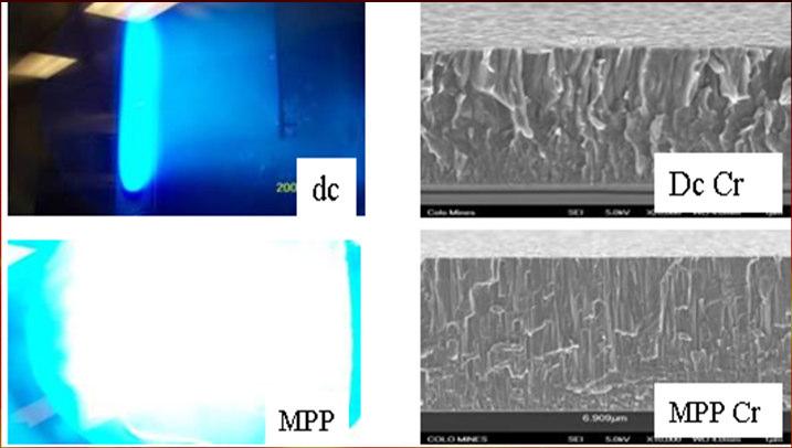
9 Film Samples Using MPP Generators Courtesy of CSM TiAlN C Cu, TiN Al2O3
10 HIPIMS/HPPMS Advantages For Magnetrons 1- High throughput( Sputtering rate equal to DC rate) 2- High Sputtering voltage ( Up to 900V) 3- Advanced Arc suppression ( Reaction time <800ns) 4-Ability to adjust pulser output to generate metal ions to improve film/layer: a. Density b. Adhesion c. Uniformity d. Stress ( compressive vs tensile) e. Roughness f. Mechanical properties g. Electrical properties h. Optical properties 5-Yields the highest rate in oxide and nitride sputtering 6-The discharge can be used as gas activation source 7-nano-layer deposition for better stress control mainly for thick layer deposition>2um ( carbon)
11 HIPMIS/HPPMS Advantages For Arc Sources 1. High throughput 2. High Ionization 3. Reduced Macro-particle Generation 4. Ability to adjust pulser output to to improve film/layer: Density Adhesion Stress ( compressive vs tensile) Roughness Mechanical properties Electrical properties 5. Oxide and Nitride depositions 6. The discharge can be used as gas activation source

12 HIPIMS/HPPMS Generator Applications We believe that the future of thin film deposition will be achieved by I-PVD; therefore, if you are in any of the following markets: Semiconductor MEMS Data Storage Hard Coatings Tribological Coatings Solar Optical Protective Coatings Others Zpulser Generators will improve your current process and/or will enable your future process development.
13 Product Road Map Developed Products: Axia ( Peak Voltage 1100V, Peak Current 250A, up to 12kW Average Power) Sputtering Solo ( Peak Voltage 1100V, Peak Current 550A, up to 22kW Average Power) Sputtering Vesta ( DC/ Pulsed DC Bias supplies up to 1000V) Coming Soon Cyprium High Voltage ( ~1700V, 50us Pulser with voltage rise time control and voltage oscillation (40%-100%)) Q Arcus ( Peak Current 250A up to 2000A, Up to 20kW) Arc Deposition Q4 2011
High Power Pulse Plasma Generators (HPPMS/HIPIMS/MPP) for Material Processing Applications. Zond, Inc / Zpulser, LLC. Mansfield, MA USA
 for Material Processing Applications. Zond, Inc / Zpulser, LLC. Mansfield, MA USA") High Power Pulse Plasma Generators (HPPMS/HIPIMS/MPP) for Material Processing Applications. Zond, Inc / Zpulser, LLC. Mansfield, MA 02048 USA Magnetron Sputtering Magnetron sputtering is a widely used
High Power Pulse Plasma Generators (HPPMS/HIPIMS/MPP) for Material Processing Applications. Zond, Inc / Zpulser, LLC. Mansfield, MA 02048 USA Magnetron Sputtering Magnetron sputtering is a widely used
SOLVIX ARC AND BIAS SERIES
 CATHODIC ARC DEPOSITION WITH PRECISE PROCESS CONTROL AND SUPERIOR FILM QUALITY Arc Units 60, 100, 210, and 400 A Bias Units 3 to 30 kw Regulation Modes Current, power, and voltage 2018 Advanced Energy
A flexible HiPIMS pulser for the latest generation of coatings
 HIPSTER 1 Pulser A flexible HiPIMS pulser for the latest generation of coatings Reactive mode HiPSTER 1 HiPIMS Pulser Our HiPSTER HiPIMS units are designed by experts in the field with an excellent track
MP 1 Unipolar Pulse Power Supply
 MP 1 Unipolar Pulse Power Supply Highest flexibility. Supreme performance for Single Magnetron sputtering processes, Plasma Nitriting Processes and Bias application. The MAGPULS Unipolar Pulse Power supplies
CLUSTERLINE RAD VERSATILE DYNAMIC SPUTTER SYSTEM OPTOELECTRONICS, MEMS, PHOTONICS, WIRELESS
 CLUSTERLINE RAD VERSATILE DYNAMIC SPUTTER SYSTEM OPTOELECTRONICS, MEMS, PHOTONICS, WIRELESS CLUSTERLINE RAD Enabling your roadmap in thin film deposition The combination of Evatec s process know-how and
Advanced Arc-Handling for HiPIMS-PS
 Advanced Arc-Handling for HiPIMS-PS Advanced ARC-Handling for HiPIMS-PS Gerhard Eichenhofer April 22, 2013 SVC TechCon 2013 is now Advanced Arc-Handling for HiPIMS-PS Advanced ARC-Handling for HiPIMS-PS
DC & PULSE Power Supplies for Plasma Process
 www.entek.kr/electronic Worldwide Sales & Service Support DC & PULSE Power Supplies for Plasma Process DC & PULSE Atmospheric Pressure Plasma Arc Ion Plating Cleaning & Bias Ion Beam OLED Heating 102-1101,
ASCENT AP (ADVANCED PULSING) POWER SUPPLIES
 POWER SUPPLIES") (ADVANCED PULSING) POWER SUPPLIES UNPRECEDENTED POWER CONTROL FOR SINGLE- AND DUAL-MAGNETRON SPUTTERING Power 30 kw (15 kw) Voltage 1000 VDC Average Current 75 A (38 A) Frequency 0, 5 to 150 khz 2018 Advanced
(ADVANCED PULSING) POWER SUPPLIES UNPRECEDENTED POWER CONTROL FOR SINGLE- AND DUAL-MAGNETRON SPUTTERING Power 30 kw (15 kw) Voltage 1000 VDC Average Current 75 A (38 A) Frequency 0, 5 to 150 khz 2018 Advanced
knowledge generating NOVEL PULSED-DC TECHNOLOGY DUAL USAGE POWER SUPPLY Background The challenge: effective application of plasma power supply
 generating knowledge NOVEL PULSED-DC TECHNOLOGY DUAL USAGE POWER SUPPLY Background The DC and Pulsed-DC sputtering is one of the most commonly used sputtering technique on the industrial scale. It is used
Plasma Power-Supply PLASMATEC
 Plasma Power-Supply PLASMATEC from DC to UNIPOLAR to BIPOLAR Plasma Power-Supply PLASMATEC SERIES OVERVIEW The PLASMATEC-Series is a highly reliable, primary switched-mode power supply product line. The
Process power from TRUMPF Hüttinger. Generators for plasma excitation.
 Process power from TRUMPF Hüttinger Generators for plasma excitation. TRUMPF Hüttinger harnesses one of nature s most awesome powers. How we are putting plasma excitation to work. We can see it in lightning,
knowledge generating HIPIMS NEW POSSIBILITIES FOR INDUSTRY Background TRUMPF Hüttinger White Paper 04/2017
 generating knowledge HIPIMS NEW POSSIBILITIES FOR INDUSTRY Figure 1: Schematic representation of the HIPIMS technology compared to DC and Pulsed-DC sputtering. In HIPIMS the same average power is delivered
Pinnacle Plus+ Pulsed-DC Power Supplies. Proven benefits for reactive-sputtering applications
 Pulsed-DC Power Supplies Proven benefits for reactive-sputtering applications Reduce the cost and complexity of oxide and nitride processes Virtually eliminate arcing Benefits Higher deposition and yield
Alameda Applied Sciences Corporation
 Alameda Applied Sciences Corporation Coaxial Energetic Deposition (CED TM ) of superconducting thin films of Nb for RF cavities* Mahadevan Krishnan, Andrew Gerhan, Kristi Wilson, Jason Wright, Brian Bures
WEAR RATE ANALYSIS OF NANO-COATED CUTTING TOOL
 WEAR RATE ANALYSIS OF NANO-COATED CUTTING TOOL Ivin S Bovas 1, Anoop M R 2 1 Mechanical department Mar Baselios College of Engineering Nalanchira, Thiruvananthapuram (India) 2 Assistant Professor, Mechanical
Gencoa 3G Circular Magnetron
 Gencoa 3G Circular Magnetron Presenting Gencoa s 3 rd generation range of circular magnetrons November 2017 www.gencoa.com 1 Contents Product Overview Introduction 3G Design Features 3G Mechanical Options
UHV ARC DEPOSITION FOR RF SUPERCONDUCTING CAVITY
 UHV ARC DEPOSITION FOR RF SUPERCONDUCTING CAVITY S. Tazzari, A. Cianchi, R. Russo, University of Rome Tor Vergata and INFN-Roma2, Rome, Italy L. Catani, INFN-Roma2, Rome, Italy F. Tazzioli, Laboratori
Dual Magnetron Sputtering of Aluminum and Silicon Oxides for Low Temperature, High Rate Processing Abstract Background
 Dual Magnetron Sputtering of Aluminum and Silicon Oxides for Low Temperature, High Rate Processing Christopher Merton and Scott Jones, 3M Corporate Research Lab, St. Paul, Minnesota, USA and Doug Pelleymounter,
TruPlasma DC Series 3000 Series 3000 (G2) Take a closer look to perfection.
 Take a closer look to perfection.") TruPlasma DC Series 3000 Series 3000 (G2) Take a closer look to perfection. TRUMPF Hüttinger driving innovations to higher levels. State-of-the-art solutions for DC sputtering. TruPlasma DC Series 3000.
TruPlasma DC Series 3000 Series 3000 (G2) Take a closer look to perfection. TRUMPF Hüttinger driving innovations to higher levels. State-of-the-art solutions for DC sputtering. TruPlasma DC Series 3000.
WHITEPAPER POWER SYSTEMS FOR REACTIVE SPUTTERING OF. By R.A. Scholl, Advanced Energy Industries, Inc.
 WHITEPAPER By R.A. Scholl, Advanced Energy Industries, Inc. POWER SYSTEMS FOR REACTIVE SPUTTERING OF There are several approaches available for deposition of insulating films, and a number of means for
Major Fabrication Steps in MOS Process Flow
 Major Fabrication Steps in MOS Process Flow UV light Mask oxygen Silicon dioxide photoresist exposed photoresist oxide Silicon substrate Oxidation (Field oxide) Photoresist Coating Mask-Wafer Alignment
RAISING THE BAR ON REACTIVE DEPOSITION SPUTTER RATES Douglas R. Pelleymounter
 RAISING THE BAR ON REACTIVE DEPOSITION SPUTTER RATES Douglas R. Pelleymounter ABSTRACT Sputtering non-conductive oxides at a high deposition rate for a long period of time has always been a goal for process
HfO 2 Based Resistive Switching Non-Volatile Memory (RRAM) and Its Potential for Embedded Applications
 and Its Potential for Embedded Applications") 2012 International Conference on Solid-State and Integrated Circuit (ICSIC 2012) IPCSIT vol. 32 (2012) (2012) IACSIT Press, Singapore HfO 2 Based Resistive Switching Non-Volatile Memory (RRAM) and Its
2012 International Conference on Solid-State and Integrated Circuit (ICSIC 2012) IPCSIT vol. 32 (2012) (2012) IACSIT Press, Singapore HfO 2 Based Resistive Switching Non-Volatile Memory (RRAM) and Its
MDX DC 1 kw & 1.5 kw Series. Tight regulation Superior arc control Low stored output energy
 MDX DC 1 kw & 1.5 kw Series Tight regulation Superior arc control Low stored output energy Benefits Tight regulation Improved yield Reduced target burn-in time High reliability Tight regulation, superior
Real time plasma etch control by means of physical plasma parameters with HERCULES
 Real time plasma etch control by means of physical plasma parameters with HERCULES A. Steinbach 1) S. Bernhard 1) M. Sussiek 4) S. Wurm 2) Ch. Koelbl 3) D. Knobloch 1) Siemens, Dresden Siemens at International
EE 143 Microfabrication Technology Fall 2014
 EE 143 Microfabrication Technology Fall 2014 Prof. Clark T.-C. Nguyen Dept. of Electrical Engineering & Computer Sciences University of California at Berkeley Berkeley, CA 94720 EE 143: Microfabrication
Niobium Coating of Copper Cavities by UHV Cathodic Arc: progress report
 Niobium Coating of Copper Cavities by UHV Cathodic Arc: progress report L. Catani, A. Cianchi, D. Digiovenale, J. Lorkiewicz, Prof. S. Tazzari, INFN-Roma "Tor Vergata", Italy Roberto Russo, Istituto di
POLYMER MICROSTRUCTURE WITH TILTED MICROPILLAR ARRAY AND METHOD OF FABRICATING THE SAME
 POLYMER MICROSTRUCTURE WITH TILTED MICROPILLAR ARRAY AND METHOD OF FABRICATING THE SAME Field of the Invention The present invention relates to a polymer microstructure. In particular, the present invention
Nanofluidic Diodes based on Nanotube Heterojunctions
 Supporting Information Nanofluidic Diodes based on Nanotube Heterojunctions Ruoxue Yan, Wenjie Liang, Rong Fan, Peidong Yang 1 Department of Chemistry, University of California, Berkeley, CA 94720, USA
Innovative Technologies for RF & Power Applications
 Innovative Technologies for RF & Power Applications > Munich > Nov 14, 2017 1 Key Technologies Key Technologies Veeco Market Focus Advanced Packaging, MEMS & RF Lighting, Display & Power Electronics Lithography
Practical Applications of Laser Technology for Semiconductor Electronics
 Practical Applications of Laser Technology for Semiconductor Electronics MOPA Single Pass Nanosecond Laser Applications for Semiconductor / Solar / MEMS & General Manufacturing Mark Brodsky US Application
HA-2520, HA-2522, HA-2525
 HA-, HA-, HA- Data Sheet September 99 File Number 9. MHz, High Slew Rate, Uncompensated, High Input Impedance, Operational Amplifiers HA-// comprise a series of operational amplifiers delivering an unsurpassed
Control of Induction Thermal Plasmas by Coil Current Modulation in Arbitrary-waveform
 J. Plasma Fusion Res. SERIES, Vol. 8 (29) Control of Induction Thermal Plasmas by Coil Current Modulation in Arbitrary-waveform Yuki TSUBOKAWA, Farees EZWAN, Yasunori TANAKA and Yoshihiko UESUGI Division
GSM OPTICAL MONITORING FOR HIGH PRECISION THIN FILM DEPOSITION
 OPTICAL MONITORING FOR HIGH PRECISION THIN FILM DEPOSITION OPTICAL MONITORING TECHNOLOGIES ENABLING OUR NEW WORLD! - ACHIEVING MORE DEMANDING THIN FILM SPECIFICATIONS - DRIVING DOWN UNIT COSTS THE GSM1101
State-of-the-art thin film X-ray optics for synchrotrons and FEL sources. Frank Hertlein Incoatec GmbH Geesthacht, Germany
 State-of-the-art thin film X-ray optics for synchrotrons and FEL sources Frank Hertlein Incoatec GmbH Geesthacht, Germany Incoatec: Innovative Coating Technologies Incoatec is founded with Bruker AXS in
Plasma Enhanced Chemical Vapor Deposition (PECVD) of Silicon Nitride (SiNx) Using Oxford Instruments System 100 PECVD
 of Silicon Nitride (SiNx) Using Oxford Instruments System 100 PECVD") University of Pennsylvania ScholarlyCommons Tool Data Browse by Type 2-28-2017 Plasma Enhanced Chemical Vapor Deposition (PECVD) of Silicon Nitride (SiNx) Using Oxford Instruments System 100 PECVD Meredith
University of Pennsylvania ScholarlyCommons Tool Data Browse by Type 2-28-2017 Plasma Enhanced Chemical Vapor Deposition (PECVD) of Silicon Nitride (SiNx) Using Oxford Instruments System 100 PECVD Meredith
A novel sputtering technique: Inductively Coupled Impulse Sputtering (ICIS)
") A novel sputtering technique: Inductively Coupled Impulse Sputtering (ICIS) LOCH, Daniel and EHIASARIAN, Arutiun Available
A novel sputtering technique: Inductively Coupled Impulse Sputtering (ICIS) LOCH, Daniel and EHIASARIAN, Arutiun Available
FOUR DIMENSIONS. Mercury Probe Systems. CVmap 92/3093 Series. CVmap 3093A System
 FOUR DIMENSIONS Mercury Probe Systems CVmap 3093A System CVmap 92/3093 Series OVERVIEW The CVmap 92/3093 Series can perform C-V plots at various frequencies up to 10MHz and/or I-V plots in wide current
High Efficient Heat Dissipation on Printed Circuit Boards. Markus Wille, R&D Manager, Schoeller Electronics Systems GmbH
 High Efficient Heat Dissipation on Printed Circuit Boards Markus Wille, R&D Manager, Schoeller Electronics Systems GmbH m.wille@se-pcb.de Introduction 2 Heat Flux: Q x y Q z The substrate (insulation)
(12) Patent Application Publication (10) Pub. No.: US 2014/ A1
 Patent Application Publication (10) Pub. No.: US 2014/ A1") (19) United States US 20140097081A1 (12) Patent Application Publication (10) Pub. No.: US 2014/0097081 A1 Morrissey et al. (43) Pub. Date: (54) METHODS OF FORMING ATHIN FILM (52) U.S. Cl. RESISTOR USPC...
(19) United States US 20140097081A1 (12) Patent Application Publication (10) Pub. No.: US 2014/0097081 A1 Morrissey et al. (43) Pub. Date: (54) METHODS OF FORMING ATHIN FILM (52) U.S. Cl. RESISTOR USPC...
Nano-structured superconducting single-photon detector
 Nano-structured superconducting single-photon detector G. Gol'tsman *a, A. Korneev a,v. Izbenko a, K. Smirnov a, P. Kouminov a, B. Voronov a, A. Verevkin b, J. Zhang b, A. Pearlman b, W. Slysz b, and R.
HA-2600, HA Features. 12MHz, High Input Impedance Operational Amplifiers. Applications. Pinouts. Ordering Information
 HA26, HA26 September 998 File Number 292.3 2MHz, High Input Impedance Operational Amplifiers HA26/26 are internally compensated bipolar operational amplifiers that feature very high input impedance (MΩ,
Crystal AC Power Supplies: 60, 100, 120, 150, and 180 kw. Mid-frequency sinusoidal power for dualmagnetron
 Crystal AC Power Supplies: 60, 100, 120, 150, and 180 kw Mid-frequency sinusoidal power for dualmagnetron reactive sputtering and PECVD Crystal AC Power SuPPlies Precise power control is essential for
V. Bellido-González 2, J. O Brien 3, P. Kelly 1 D. Arnell 1, D. Monaghan 2
 Application of Fourier Transform Analysis to Pulsed Magnetr on Sputter ing Technology V. Bellido-González 2, J. O Brien 3, P. Kelly 1 D. Arnell 1, D. Monaghan 2 1 Salford University, IMR (UK) 2 Gencoa
OPERATING THE HIPIMS DISCHARGE WITH ULTRA-SHORT PULSES: A SOLUTION TO OVERCOME THE DEPOSITION RATE LIMITATION
 Romanian Reports in Physics 69, 411 (2017) OPERATING THE HIPIMS DISCHARGE WITH ULTRA-SHORT PULSES: A SOLUTION TO OVERCOME THE DEPOSITION RATE LIMITATION I.-L. VELICU 1, I. MIHAILA 2, G. POPA 1 1 Alexandru
High efficiency RF matching network for ICP sources in industrial applications
 High efficiency RF matching network for ICP sources in industrial applications Dr. Rudolf Beckmann (Manz Coating GmbH) Dr. Roland Gesche, Joachim Scherer (Aurion Anlagentechnik GmbH) Introduction Why aren
HA-2520, HA MHz, High Slew Rate, Uncompensated, High Input Impedance, Operational Amplifiers. Features. Applications. Ordering Information
 HA-22, HA-22 Data Sheet August, 2 FN2894. 2MHz, High Slew Rate, Uncompensated, High Input Impedance, Operational Amplifiers HA-22/22 comprise a series of operational amplifiers delivering an unsurpassed
Semiconductor Materials for Power Electronics (SEMPEL) GaN power electronics materials
 GaN power electronics materials") Semiconductor Materials for Power Electronics (SEMPEL) GaN power electronics materials Kjeld Pedersen Department of Physics and Nanotechnology, AAU SEMPEL Semiconductor Materials for Power Electronics
Semiconductor Materials for Power Electronics (SEMPEL) GaN power electronics materials Kjeld Pedersen Department of Physics and Nanotechnology, AAU SEMPEL Semiconductor Materials for Power Electronics
Supplementary Information
 Supplementary Information Wireless thin film transistor based on micro magnetic induction coupling antenna Byoung Ok Jun 1, Gwang Jun Lee 1, Jong Gu Kang 1,2, Seung Uk Kim 1, Ji Woong Choi 1, Seung Nam
The Department of Advanced Materials Engineering. Materials and Processes in Polymeric Microelectronics
 The Department of Advanced Materials Engineering Materials and Processes in Polymeric Microelectronics 1 Outline Materials and Processes in Polymeric Microelectronics Polymeric Microelectronics Process
(12) Patent Application Publication (10) Pub. No.: US 2011/ A1
 Patent Application Publication (10) Pub. No.: US 2011/ A1") (19) United States US 20110165057A1 (12) Patent Application Publication (10) Pub. No.: US 2011/0165057 A1 Honda et al. (43) Pub. Date: (54) PLASMACVD DEVICE, DLC FILM, AND C23C I6/455 (2006.01) METHOD
(19) United States US 20110165057A1 (12) Patent Application Publication (10) Pub. No.: US 2011/0165057 A1 Honda et al. (43) Pub. Date: (54) PLASMACVD DEVICE, DLC FILM, AND C23C I6/455 (2006.01) METHOD
DYNAMICS OF NONLINEAR PLASMA-CIRCUIT INTERACTION *
 Seminar in Plasma Aided Manufacturing University of Wisconsin, Madison, Wisconsin September 18, 1998. DYNAMICS OF NONLINEAR PLASMA-CIRCUIT INTERACTION * SHAHID RAUF Department of Electrical & Computer
In their earliest form, bandpass filters
 Bandpass Filters Past and Present Bandpass filters are passive optical devices that control the flow of light. They can be used either to isolate certain wavelengths or colors, or to control the wavelengths
PROCEEDINGS OF SPIE. LPP-EUV light source for HVM lithography. T. Saito, Y. Ueno, T. Yabu, A. Kurosawa, S. Nagai, et al.
 PROCEEDINGS OF SPIE SPIEDigitalLibrary.org/conference-proceedings-of-spie LPP-EUV light source for HVM lithography T. Saito, Y. Ueno, T. Yabu, A. Kurosawa, S. Nagai, et al. Invited Paper LPP-EUV light
GST CMP BLANKET and TEST PATTERNED WAFERS
 C M P C h a r a c t e r I z a t I o n S o l u t I o n s GST CMP BLANKET and TEST PATTERNED WAFERS MARCH 20, 2009 PREPARED BY SOOKAP HAHN PRESIDENT SKW ASSOCIATES, INC. 2920 SCOTT BOULEVARD SANTA CLARA,
Department of Astronomy, Graduate School of Science, the University of Tokyo, Hongo, Bunkyo-ku, Tokyo , Japan;
 Verification of the controllability of refractive index by subwavelength structure fabricated by photolithography: toward single-material mid- and far-infrared multilayer filters Hironobu Makitsubo* a,b,
State-of-the-art device fabrication techniques
 State-of-the-art device fabrication techniques! Standard Photo-lithography and e-beam lithography! Advanced lithography techniques used in semiconductor industry Deposition: Thermal evaporation, e-gun
A DC POST-MAGNETRON CONFIGURATION FOR NIOBIUM SPUTTERING INTO 1.5 GHz COPPER MONOCELLS.
 A DC POST-MAGNETRON CONFIGURATION FOR NIOBIUM SPUTTERING INTO 1.5 GHz COPPER MONOCELLS. V. PALMIERI, R. PRECISO, V.L. RUZINOV A, S.Yu. STARK A ISTITUTO NAZIONALE DI FISICA NUCLEARE Laboratori Nazionali
2017 Advanced Energy Industries, Inc. PEII SERIES LOW-FREQUENCY POWER SUPPLIES 5 TO 60 KW
 2017 Advanced Energy Industries, Inc. PEII SERIES LOW-FREQUENCY POWER SUPPLIES 5 TO 60 KW Enhanced arc control with internal load matching for 40 khz reactive sputtering applications Page 2 The PEII power
Instrument Catalogue
 Instrument Catalogue Table of Contents Substrate Level Measurement 6 Semion System Ion Energy, Ion Flux and Uniformity Analysis 8 Vertex System Ion Energy Distribution 10 Quantum System Ion & Neutral Deposition
State-of-The-Art Dielectric Etch Technology
 State-of-The-Art Dielectric Etch Technology Koichi Yatsuda Product Marketing Manager Etch System Business Unit November 5 th, 2010 TM Outline Dielectric Etch Challenges for State-of-The-Art Devices Control
Gas Detectors for μ systems
 Gas Detectors for μ systems Marcello Piccolo SNOWMASS August 2005 μ system requirements for gaseous detectors Given the design we have seen up to now, a muon system should comprise a detector that; Is
SUPPLEMENTARY INFORMATION
 A transparent bending-insensitive pressure sensor Sungwon Lee 1,2, Amir Reuveny 1,2, Jonathan Reeder 1#, Sunghoon Lee 1,2, Hanbit Jin 1,2, Qihan Liu 5, Tomoyuki Yokota 1,2, Tsuyoshi Sekitani 1,2,3, Takashi
Ion beam etch and deposition systems
 Ion beam etch and deposition systems The Business of Science Ion beam systems Ion beam technology offers unique abilities in etch and deposition Oxford Instruments offers a single tool, allowing the flexibility
Technology for the MEMS processing and testing environment. SUSS MicroTec AG Dr. Hans-Georg Kapitza
 Technology for the MEMS processing and testing environment SUSS MicroTec AG Dr. Hans-Georg Kapitza 1 SUSS MicroTec Industrial Group Founded 1949 as Karl Süss KG GmbH&Co. in Garching/ Munich San Jose Waterbury
Flexible IGZO TFTs deposited on PET substrates using magnetron radio frequency co-sputtering system
 The 2012 World Congress on Advances in Civil, Environmental, and Materials Research (ACEM 12) Seoul, Korea, August 26-30, 2012 Flexible IGZO TFTs deposited on PET substrates using magnetron radio frequency
Hermetic Packaging Solutions using Borosilicate Glass Thin Films. Lithoglas Hermetic Packaging Solutions using Borosilicate Glass Thin Films
 Hermetic Packaging Solutions using Borosilicate Glass Thin Films 1 Company Profile Company founded in 2006 ISO 9001:2008 qualified since 2011 Headquarters and Production in Dresden, Germany Production
CMP for More Than Moore
 2009 Levitronix Conference on CMP Gerfried Zwicker Fraunhofer Institute for Silicon Technology ISIT Itzehoe, Germany gerfried.zwicker@isit.fraunhofer.de Contents Moore s Law and More Than Moore Comparison:
Supporting Information for. Thin, Lightweight, Foldable Thermochromic Displays on Paper
 Supporting Information for Thin, Lightweight, Foldable Thermochromic Displays on Paper Adam C. Siegel, Scott T. Phillips, Benjamin Wiley, and George M. Whitesides Department of Chemistry and Chemical Biology,
Y S. C 2. United States Patent (19) Sellers Y S S K, % NS, SAS, WAZ. 11 Patent Number: 5,810,982 (45) Date of Patent: *Sep. 22, NZ MN 1
 Sellers Y S S K, % NS, SAS, WAZ. 11 Patent Number: 5,810,982 (45) Date of Patent: *Sep. 22, NZ MN 1") United States Patent (19) Sellers 54 PREFERENTIAL SPUTTERING OF INSULATORS FROM CONDUCTIVE TARGETS 75 Inventor: Jeff C. Sellers, Palmyra, N.Y. 73 Assignee: ENI Technologies, Inc., Rochester, N.Y. * Notice:
United States Patent (19) Sellers 54 PREFERENTIAL SPUTTERING OF INSULATORS FROM CONDUCTIVE TARGETS 75 Inventor: Jeff C. Sellers, Palmyra, N.Y. 73 Assignee: ENI Technologies, Inc., Rochester, N.Y. * Notice:
Session 3: Solid State Devices. Silicon on Insulator
 Session 3: Solid State Devices Silicon on Insulator 1 Outline A B C D E F G H I J 2 Outline Ref: Taurand Ning 3 SOI Technology SOl materials: SIMOX, BESOl, and Smart Cut SIMOX : Synthesis by IMplanted
ESD Sensitivity of Precision Chip Resistors Comparison between Foil and Thin Film Chips
 VISHAY FOIL RESISTORS Resistive Products Technical Note By Joseph Szwarc, 2008 ABSTRACT The sensitivity level of resistors used in electronic equipment to an electrostatic discharge (ESD) varies from a
Etch, Deposition, and Metrology Options for Cost-Effective Thin-Film Bulk Acoustic Resonator (FBAR) Production
 Production") Etch, Deposition, and Metrology Options for Cost-Effective Thin-Film Bulk Acoustic Resonator (FBAR) Production Figure 1 Veeco is driving System on a Chip Technology Frank M. Cumbo, Kurt E. Williams, John
Etch, Deposition, and Metrology Options for Cost-Effective Thin-Film Bulk Acoustic Resonator (FBAR) Production Figure 1 Veeco is driving System on a Chip Technology Frank M. Cumbo, Kurt E. Williams, John
E3, ES 2.ÉAN 27 Asiaz
 (19) United States US 2014001 4915A1 (12) Patent Application Publication (10) Pub. No.: US 2014/0014.915 A1 KOO et al. (43) Pub. Date: Jan. 16, 2014 (54) DUAL MODE DISPLAY DEVICES AND Publication Classification
EUV Light Source The Path to HVM Scalability in Practice
 EUV Light Source The Path to HVM Scalability in Practice Harald Verbraak et al. (all people at XTREME) 2011 International Workshop on EUV and Soft X-ray Sources Nov. 2011 Today s Talk o LDP Technology
Radiation Detection Instrumentation
 Radiation Detection Instrumentation Principles of Detection and Gas-filled Ionization Chambers Neutron Sensitive Ionization Chambers Detection of radiation is a consequence of radiation interaction with
- Datasheet - Features: Version 1.1. Cryogenic Low Pass Filter Unit Type KA-Fil 2a
 Cryogenic Low Pass Filter Unit Type KA-Fil 2a - Datasheet - Version 1.1 Features: 5 Independent Low Pass Filters Operating Range 300K to 4.2K Overriding Diodes allow Bypassing and Pulsing Small Size 2009
A Laser-Based Thin-Film Growth Monitor
 TECHNOLOGY by Charles Taylor, Darryl Barlett, Eric Chason, and Jerry Floro A Laser-Based Thin-Film Growth Monitor The Multi-beam Optical Sensor (MOS) was developed jointly by k-space Associates (Ann Arbor,
(a) (d) (e) (b) (c) (f) 3D-NAND Flash and Its Manufacturing Process
 (d) (e) (b) (c) (f) 3D-NAND Flash and Its Manufacturing Process") 3D-NAND Flash and Its Manufacturing Process 79 (d) Si Si (b) (c) (e) Si (f) +1-2 (g) (h) Figure 2.33 Top-down view in cap oxide and (b) in nitride_n-2; (c) cross-section near the top of the channel; top-down
3D-NAND Flash and Its Manufacturing Process 79 (d) Si Si (b) (c) (e) Si (f) +1-2 (g) (h) Figure 2.33 Top-down view in cap oxide and (b) in nitride_n-2; (c) cross-section near the top of the channel; top-down
HipoCIGS: enamelled steel as substrate for thin film solar cells
 HipoCIGS: enamelled steel as substrate for thin film solar cells Lecturer D. Jacobs*, Author S. Efimenko, Co-author C. Schlegel *:PRINCE Belgium bvba, Pathoekeweg 116, 8000 Brugge, Belgium, djacobs@princecorp.com
PROFILE CONTROL OF A BOROSILICATE-GLASS GROOVE FORMED BY DEEP REACTIVE ION ETCHING. Teruhisa Akashi and Yasuhiro Yoshimura
 Stresa, Italy, 25-27 April 2007 PROFILE CONTROL OF A BOROSILICATE-GLASS GROOVE FORMED BY DEEP REACTIVE ION ETCHING Teruhisa Akashi and Yasuhiro Yoshimura Mechanical Engineering Research Laboratory (MERL),
Measuring the Ion Current to the Substrate During Deposition of Thin Films by Hollow Cathode Plasma Jet
 WDS'07 Proceedings of Contributed Papers, Part II, 212 217, 2007. ISBN 978-80-7378-024-1 MATFYZPRESS Measuring the Ion Current to the Substrate During Deposition of Thin Films by Hollow Cathode Plasma
Managing Arcs for Optimum Deposition Performance
 Managing Arcs for Optimum Deposition Performance D. Carter and H. Walde, Advanced Energy Industries Inc., Fort Collins, CO ABSTRACT Over the years a broad range of arc detection and power supply response
Figure 1. Physical Photo of AHV12V10KV1MAW
 Figure 1. Physical Photo of FEATURES High precision Full modulation range on output voltage Linear regulation Shutdown APPLICATIONS This power module,, is designed for achieving DC-DC conversion from low
PHGN/CHEN/MLGN 435/535: Interdisciplinary Silicon Processing Laboratory. Simple Si solar Cell!
 Where were we? Simple Si solar Cell! Two Levels of Masks - photoresist, alignment Etch and oxidation to isolate thermal oxide, deposited oxide, wet etching, dry etching, isolation schemes Doping - diffusion/ion
Piezoelectric Lead Zirconate Titanate (PZT) Ring Shaped Contour-Mode MEMS Resonators
 Ring Shaped Contour-Mode MEMS Resonators") IOP Conference Series: Materials Science and Engineering PAPER OPEN ACCESS Piezoelectric Lead Zirconate Titanate (PZT) Ring Shaped Contour-Mode MEMS Resonators To cite this article: P.V. Kasambe et al
IOP Conference Series: Materials Science and Engineering PAPER OPEN ACCESS Piezoelectric Lead Zirconate Titanate (PZT) Ring Shaped Contour-Mode MEMS Resonators To cite this article: P.V. Kasambe et al
Precision Cold Ablation Material Processing using High-Power Picosecond Lasers
 Annual meeting Burgdorf Precision Cold Ablation Material Processing using High-Power Picosecond Lasers Dr. Kurt Weingarten kw@time-bandwidth.com 26 November 2009 Background of Time-Bandwidth Products First
HA MHz, High Slew Rate, High Output Current Buffer. Description. Features. Applications. Ordering Information. Pinouts.
 SEMICONDUCTOR HA-2 November 99 Features Voltage Gain...............................99 High Input Impedance.................... kω Low Output Impedance....................... Ω Very High Slew Rate....................
Figure 1. Physical Photo of AHV12VN10KV1MAW
 Figure 1. Physical Photo of FEATURES High precision Full modulation range on output voltage Negative voltage output Linear regulation Shutdown APPLICATIONS This power module,, is designed for achieving
Multi-Wire Drift Chambers (MWDC)
") Multi-Wire Drift Chambers (MWDC) Mitra Shabestari August 2010 Introduction The detailed procedure for construction of multi-wire drift chambers is presented in this document. Multi-Wire Proportional Counters
Multi-Wire Drift Chambers (MWDC) Mitra Shabestari August 2010 Introduction The detailed procedure for construction of multi-wire drift chambers is presented in this document. Multi-Wire Proportional Counters
Micro-sensors - what happens when you make "classical" devices "small": MEMS devices and integrated bolometric IR detectors
 Micro-sensors - what happens when you make "classical" devices "small": MEMS devices and integrated bolometric IR detectors Dean P. Neikirk 1 MURI bio-ir sensors kick-off 6/16/98 Where are the targets
MULTI-FREQUENCY OPERATION OF RIE AND ICP SOURCES *
 45th International Symposium of the American Vacuum Society Baltimore, Maryland November 2-6, 1998. MULTI-FREQUENCY OPERATION OF RIE AND ICP SOURCES * Shahid Rauf and Mark J. Kushner Department of Electrical
Enable Highly-Stable Plasma Operations at High Pressures with the Right RPS Solution
 Enable Highly-Stable Plasma Operations at High Pressures with the Right RPS Solution Created by Advanced Energy Industries, Inc., Fort Collins, CO Abstract Conventional applications for remote plasma sources
by Radio Frequency Self-Bias
 THE SCIENCE AND ENGINEERING REVIEW OF DOSHISHA UNIVERSITY, VOL. 51, NO. 2 July 2010 Sputtering of Liquid Metal Suspended on an Insulating Reservoir by Radio Frequency Self-Bias Magdaleno R. VASQUEZ Jr.
INTRODUCTION TO MOS TECHNOLOGY
 INTRODUCTION TO MOS TECHNOLOGY 1. The MOS transistor The most basic element in the design of a large scale integrated circuit is the transistor. For the processes we will discuss, the type of transistor
Correspondence should be addressed to Shojiro Miyake;
 Nanomaterials Volume 214, Article ID 657619, 13 pages http://dx.doi.org/1.1155/214/657619 Research Article Regression Analysis of the Effect of Bias Voltage on Nano- and Macrotribological Properties of
Electronic component
 Electronic component Electronic component: An electronic component is any basic discrete device or physical entity in an electronic system used to affect electrons or their associated fields. 2 TYPES OF
Quasi Active High Power L Band PIN Diode Limiter Module - SMT. Surface Mount L- Band Limiter Module: High Peak Power Handling: Low Insertion Loss:
 PRELIMINARY RFLM-102202XA-150 Quasi Active High Power L Band PIN Diode Limiter Module - SMT Features: Surface Mount L- Band Limiter Module: Frequency Range: High Average Power Handling: High Peak Power
(12) Patent Application Publication (10) Pub. No.: US 2017/ A1
 Patent Application Publication (10) Pub. No.: US 2017/ A1") (19) United States US 20170017025A1 (12) Patent Application Publication (10) Pub. No.: US 2017/0017025 A1 JIDA et al. (43) Pub. Date: (54) OPTICAL FILTER AND IMAGING DEVICE (71) Applicant: KONICA MINOLTA,
(19) United States US 20170017025A1 (12) Patent Application Publication (10) Pub. No.: US 2017/0017025 A1 JIDA et al. (43) Pub. Date: (54) OPTICAL FILTER AND IMAGING DEVICE (71) Applicant: KONICA MINOLTA,
CHAPTER 1 INTRODUCTION. the sectors of industrial and customer products [5]. The first ever concept of nanotechnology
![CHAPTER 1 INTRODUCTION. the sectors of industrial and customer products [5]. The first ever concept of nanotechnology](/thumbs/86/94425600.jpg "CHAPTER 1 INTRODUCTION. the sectors of industrial and customer products [5]. The first ever concept of nanotechnology") CHAPTER 1 INTRODUCTION 1.1 General Introduction: Nanotechnology is defined as the application of nanoscience in technological devices/processes/products. It is fast promising technology capable of impacting
CHAPTER 1 INTRODUCTION 1.1 General Introduction: Nanotechnology is defined as the application of nanoscience in technological devices/processes/products. It is fast promising technology capable of impacting