Analog Electronics Circuits. Chapter 1: Diode circuits
|
|
|
- Marshall Reed
- 6 years ago
- Views:
Transcription
1 Analog Electronics Circuits Objective Chapter 1: Diode circuits To understand the diode operation and its equivalent circuits To understand various parameters of diodes Load line analysis Diode applications in rectifiers; HWR,FWR Diode testing Zener diode Diode data sheets and specifications Diode applications in clipper circuits Numerical Semiconductor diode Fig a semiconductor diode symbol
2 Basic operation n-type versus p-type Fig b Vi characteristics of a diode n-type materials make the Silicon (or Germanium) atoms more negative. p-type materials make the Silicon (or Germanium) atoms more positive. Join n-type and p-type doped Silicon (or Germanium) to form a p-n junction. p-n junction When the materials are joined, the negatively charged atoms of the n-type doped side are attracted to the positively charged atoms of the p-type doped side. The electrons in the n-type material migrate across the junction to the p-type material (electron flow). the holes in the p-type material migrate across the junction to the n-type material (conventional current flow). The result is the formation of a depletion layer around the junction. Depletion region


3 Operating conditions No Bias Forward Bias Reverse Bias No bias condition No external voltage is applied: VD = 0V and no current is flowing ID = 0A. Reverse bias condition Only a modest depletion layer exists External voltage is applied across the p-n junction in the opposite polarity of the p- and n- type materials. This causes the depletion layer to widen. The electrons in the n-type material are attracted towards the positive terminal and the holes in the p-type material are attracted towards the negative terminal.
4 Avalanche breakdown Avalanche breakdown occurs when a high reverse voltage is applied to a diode and large electric field is created across the depletion region. The effect is dependant on the doping levels in the region of the depletion layer. Minority carriers in the depletion region associated with small leakage currents are accelerated by the field to high enough energies so that they ionise silicon atoms when they collide with them. A new hole-electron pair are created which accelerate in opposite directions causing further collisions and ionisation and avalanche breakdown Zener breakdown Breakdown occurs with heavily doped junction regions (ie. highly doped regions are better conductors). If a reverse voltage is applied and the depletion region is too narrow for avalanche breakdown (minority carriers cannot reach high enough energies over the distance traveled ) the electric field will grow. However, electrons are pulled directly from the valence band on the P side to the conduction band on the N side. This type of breakdown is not destructive if the reverse current is limited. Forward Bias Condition External voltage is applied across the p-n junction in the same polarity of the p- and n- type materials. The depletion layer is narrow. The electrons from the n-type material and holes from the p-type material have sufficient energy to cross the junction. Actual v-i characteristics is as shown in fig below
![Diode current expression: ID = Is( evd / VT-1) Is : Reverse saturation current q : Charge of an electron k : Boltzman constant 11600/η T : Environment temperature in K [ K = C + 273 ] η =2 for](/docs-images/74/71356892/images/5-0.jpg "silicon, η=1 for Germanium Majority and Minority Carriers in Diode A diode, as any semiconductor device is not perfect!")
5 Diode current expression: ID = Is( evd / VT-1) Is : Reverse saturation current q : Charge of an electron k : Boltzman constant 11600/η T : Environment temperature in K [ K = C ] η =2 for silicon, η=1 for Germanium Majority and Minority Carriers in Diode A diode, as any semiconductor device is not perfect! There are two sets of currents: Majority Carriers The electrons in the n-type and holes in the p-type material are the source of the majority of the current flow in a diode. Minority Carriers Electrons in the p-type and holes in the n-type material are rebel currents. They produce a small amount of opposing current.
6 Zener Region Zener diode operation: Zener region The diode is in the reverse bias condition. At some point the reverse bias voltage is so large the diode breaks down. The reverse current increases dramatically. This maximum voltage is called avalanche breakdown voltage and the current is called avalanche current. Forward Bias Voltage No Bias condition to Forward Bias condition happens when the electron and holes are given sufficient energy to cross the p-n junction. This energy comes from the external voltage applied across the diode. The Forward bias voltage required for a Silicon diode VT 0.7V Germanium diode VT 0.3V
7 Temperature Effects on performance of diode As temperature increases it adds energy to the diode. It reduces the required Forward bias voltage in Forward Bias condition It increases the amount of Reverse current in Reverse Bias condition It increases maximum Reverse Bias Avalanche Voltage Germanium diodes are more sensitive to temperature variations than Silicon Diodes. Resistance Levels Semiconductors act differently to DC and AC currents. There are 3 types of resistances. DC or Static Resistance AC or Dynamic Resistance Average AC Resistance
8 DC or Static Resistance DC or static resistance RD=VD / ID For a specific applied DC voltage VD, the diode will have a specific current ID, and a specific resistance RD. The amount of resistance RD, depends on the applied DC voltage. AC or Dynamic Resistance
9 Forward Bias region: The resistance depends on the amount of current (ID) in the diode. Rd= vd/ Id The resistance depends on the amount of current (ID) in the diode. The voltage across the diode is fairly constant (VT = 26mV for 25 C). Reverse Bias region: Rd= The resistance is essentially infinite. The diode acts like an open. Average AC Resistance Rac= Vd/ Id Point to point
10 Diode equivalent circuits An equivalent circuit is a combination of elements properly chosen to best represent the actual terminal characteristics of a device, system or such a particular operating region. Then device symbol can be replaced with the equivalent circuit which makes the analysis of the circuit easy and straight forward. Piece wise linear equivalent circuit One technique for obtaining equivalent circuit is to approximate the characteristics of the device by straight line segments Rd defines the resistance level of the device when it is in the ON state. Ideal diode is included to establish that there is only one direction of conduction through the device. Since silicon semiconductor diode does not conduct until VD of 0.7V is reached, a battery opposing the conduction direction is included. Simplified equivalent circuit In most of the applications, resistance r av is very small in comparison to the other elements of the network. Removal of this r av from the network makes a simplified equivalent circuit. And an ideal diode will start conduction for zero applied voltage.
 However this can not be neglected in very high frequencies since it introduces a")
11 Transition and diffusion capacitance The figure shows the capacitance v/s applied voltage across the diode. Shunt capacitive effects that can be ignored at very lower frequencies since Xc=1/2πfc is very large (open circuit) However this can not be neglected in very high frequencies since it introduces a low reactance (shorting) path. Two types of capacitive effects to be considered in FB and RB condition. In RB region transition or depletion region capacitance CT in FB diffusion capacitance CD or storage capacitance. W.k.t C=εA/d. ε is the permittivity of dielectric between tow plates of area A separated by distance d. In RB, depletion region which is free of carriers that behaves essentially like an insulator between the layers of opposite charges. This depletion region width increase with increase in RB potential. Since d is increasing, capacitance effect is more in FB.
12 Diode characteristics Diode characteristics Reverse recovery time Denoted by trr. In FB condition, large number of electrons from n-type progressing through p-type and large number of holes in p-type is a requirement for conduction. The electrons in p-type and holes progressing through n-type establish a large number of minority carriers in each material. Now if the diode is changed from FB to RB
13 The diode will not instantaneously react to this sudden change. Because of the large number of minority carriers in each material, the current sustains in diode for a time ts storage time which is required for minority carriers to return to their majority carrier state in the opposite material. Eventually current will reduce to non conduction levels. This time is tt transition interval Hence trr= ts + tt This is very important consideration in high frequency operation. Commercially available diodes have reverse recovery time of few nano seconds to 1micro second. Load line Analysis The applied load will normally have an important impact on region of operation of device. If analysis is done in graphical approach, a line can be drawn on the characteristics of the device that represents applied load. The intersection of load line with the characteristics will determine the point of operation. Such an analysis is called as load-line analysis. The intersection point is called Q point or operating point.
14 Its very simple as compared to the non-linear analysis of diode which involves heavy maths i R i D By KVL : By Both KVL and KCL must be satisfied at all times i-v curves plotted for diode (energised by Vss) i-v curves plotted for resistor KCL :i V R SS i Ri D D v D
15 When v 0; We can combine these curves on one plot to do a load line analysis Load line analysis D i R VSS R i D V SS v R D When v D V SS ; By KVL : By i R KCL :i V 0 R SS Ri i D D v D
16 Example on load line analysis i R i D and i D = V SS /R = 20mA Assume : When v i D = 12.5mA v D = 1.25V i D = 0 Operating Point: KVL and KCL satisfied i i R When R R 150. v D i D i D D V SS 0 : VSS 20mA R V : 0 3V SS
17 Diode approximations In the approximate model of diode, the r av is not used since the value of this r av is much less than other series elements of the network. This model results in less expenditure of time and effort to obtain results. Unless otherwise mentioned this approximate model is used hereforth Series diode configuration with DC inputs When connected to voltage sources in series, the diode is on if the applied voltage is in the direction of forward-bias and it is greater than the VT of the diode When a diode is on, we can use the approximate model for the on state Series diode configuration Here, VD = VT, VR = E - VT ID = IR = VR / R
18 Here, VD = E, VR = 0, ID = 0 Keep in mind that KVL has to be satisfied under all conditions Parallel diode configuration Determine I1, VD1, VD2 and V0 for the parallel diode circuit in below figure
19 Solution
20 Examples 1. Find diode current and output voltage Solution: 2. Solve for I, v1,v2 and vo
21 3.Determine unknown parameters 4.Determine unknown parameters 5.Determine unknown parameters
22 Rectifiers : Half wave rectification For the half-wave rectified signal: Vdc = Vm If the effect of VT is also considered, the output of the system will as below Vdc = (Vm- VT)

23 Effect of VT on half-wave rectified signal PIV rating of Half-wave Rectifiers PIV rating is very important consideration for rectifier circuits For the half-wave rectifier must be equal or must not exceed the peak value of the applied voltage PIV Vm This is the voltage rating that must not be exceeded in the reverse bias region When vin is negative.
24 Non Ideal Waveform Half-wave Rectifier The total effect of diode on the output signal is given in below Average voltage V AV The average d.c. value of this half-wave-rectified sine wave is V AV 1 VM sind VM VM cos cos0 2
25 Full-wave Rectifiers Bridge Working : For the positive half of the AC cycle: Diode D1 and D2 gets forward biased and conducts. Working : For the negative half of the AC cycle Diode D3 and D4 gets forward biased and conducts during this half cycle.
26 Details of working of FWR We initially consider the diodes to be ideal, such that V C =0 and R f =0 The four-diode bridge can be bought as a package During positive half cycles v i is positive. Current is conducted through diodes D1, resistor R and diode D2 Meanwhile diodes D3 and D4 are reverse biased During negative half cycles v i is negative. Current is conducted through diodes D3, resistor R and diode D4 Meanwhile diodes D1 and D2 are reverse biased. Current always flows the same way through the load R. the average d.c. value of this full-wave-rectified sine wave is V AV = 2V M / (i.e. twice the half-wave value) Two diodes are in the conduction path. Thus in the case of non-ideal diodes v o will be lower than v i by 2V C. As for the half-wave rectifier a reservoir capacitor can be used. In the full wave case the discharge time is T/2 and
27 VMT ΔV 2RC Centre - tap FWR Two diodes and a center-tapped transformer are required. VDC = 0.636(Vm) Note that Vm here is the transformer secondary voltage to the tap. Operation For the positive half of the AC cycle:

28 For the negative half of the AC cycle: Summary Note: Vm = peak of the AC voltage.
29 Application of diode as Clippers Clippers have ability to clip/remove off a portion of the input signal without distorting the remaining part of the alternating waveform. HWR is simplest form of clippers. The orientation of diode is going to decide the part of sinusoidal waveform to be clipped off. Clipper configuration Depending on the way in which the diodes are connected with the input, the clipper are classified in to two major categories, viz., Series configuration Parallel configuration 1. Series clipper example 1 2. Series Clipper example 2
30 3. Series clipper ex 3 & 4 4. Series clipper Ex - 5 & 6
31 Various clipepr examples along with transfer characteristics Biased parallel clippers

32 Diode testing : 1. Diode testing using multi-meter One problem with using an ohmmeter to check a diode is that the readings obtained only have qualitative value, not quantitative. In other words, an ohmmeter only tells you which way the diode conducts; the low-value resistance indication obtained while conducting is useless. If an ohmmeter shows a value of 1.73 ohms while forward-biasing a diode, that figure of 1.73 Ω doesn't represent any real-world quantity useful to us as technicians or circuit designers. It neither represents the forward voltage drop nor any bulk resistance in the semiconductor material of the diode itself, but rather is a figure dependent upon both quantities and will vary substantially with the particular ohmmeter used to take the reading. For this reason, some digital multimeter manufacturers equip their meters with a special diode check function which displays the actual forward voltage drop of the diode in volts, rather than a resistance figure in ohms. These meters work by forcing a small current through the diode and measuring the voltage dropped between the two test leads. (Figure below)
33 Meter with a Diode check function displays the forward voltage drop of volts instead of a low resistance. The forward voltage reading obtained with such a meter will typically be less than the normal drop of 0.7 volts for silicon and 0.3 volts for germanium, because the current provided by the meter is of trivial proportions. If a multimeter with diode-check function isn't available, or you would like to measure a diode's forward voltage drop at some nontrivial current, the circuit of Figure below may be constructed using a battery, resistor, and voltmeter Measuring forward voltage of a diode without diode check meter function: (a) Schematic diagram. (b) Pictorial diagram
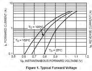
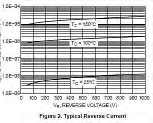
34 2. Curve tracers A curve tracer can display the characteristics of a host device. Device could be diode or transistor or other semiconductor device. Diode specifications Curve tracer by tektronix and other companies available Easy to use and testing with less effort and time. Data sheets provide data on specific semiconductor device. Manufacturers provide these information Usually given in easy readable formats like graphs, artwork, tables and so on., These specifications are required for proper utilization of devices for specific applications Important data to be considered are The forward voltage V F (at specific T) Maximum forward current I F Maximum reverse saturation current I R The reverse voltage rating (PIV) Maximum power dissipation Capacitance levels Reverse recovery time t rr Operating temperature range Depending on type of diode being used, additional data such as Frequency Noise level Switching time Thermal resistance Peak repetitive values are also provided


35 For IN4001 and 4007 Maximum ratings are those values beyond which device damage can occur.
36

37 Zener diodes By proper doping of the silicon, the Zener Breakdown can be made to have a very sharp breakdown. The breakdown voltage is commonly labeled as VZ. Characteristics of Zener diode Equivalent circuit consist of a constant voltage supply of V Z in series with a zener resistor r Z.
38 The approximate model is obtained just by neglecting the effect of r Z in the equivalent model. Only a constant voltage source is used in this model. The temperature coefficients reflects the percentage change in V Z with temperature and it is defined by the relation T c ={ V Z / V Z ( T 1 -T 0 ) } x 100% V Z change in zener potential due to temperature variation (T 1 -T 0 ) change in temperature Examples 1. Det. Nominal voltage for 1N961 fairchild zener diode at temp of c. Solution: V Z =T c V Z (T 1 -T 0 )/100 ={0.072x10V/100}( ) = 0.54V Therefore change in Zener voltage is 10.54V when temperature is raised from 25 0 c to c. 2. Find Is and vl using zener characteristics for given data. 3. Compute the Thevenin equivalent of the previous circuit with the zener diode as the load Thevenin voltage Thevenin resistance We can then write VT +RTiD+vD = 0 and find out vd,, id using the zener diode characteristics
39 vl = vd and IS = vl /RL + id Solution Answers vl = 10V IS = vl /RL + id = 10/6 +10 ma = 11.67mA vl = 9.5 V IS = vl /RL + id = 9.5/ ma = 12.92mA
40 4. Find currents through diode D1 and D2. General Approach: Assume the state of each of the diodes: i.e., on or off. Analyze the circuit and check to see if your assumptions were correct. If not correct try another set of assumptions. Assume D1 is off : Replace with open Assume D2 is on : Replace with short vd1 = 10V 3V = 7V But this is not possible since the D1 would be forward biased or on with vd1 = 0V. We must try another set of assumptions Assume D1 is on and D2 is off
41 Example 2
42 Chapter 2. - DC Biasing - BJTs Objectives To Understand : Concept of Operating point and stability Analyzing Various biasing circuits and their comparison with respect to stability BJT A Review Invented in 1948 by Bardeen, Brattain and Shockley Contains three adjoining, alternately doped semiconductor regions: Emitter (E), Base (B), and Collector (C) The middle region, base, is very thin Emitter is heavily doped compared to collector. So, emitter and collector are not interchangeable. Three operating regions Linear region operation: Base emitter junction forward biased Base collector junction reverse biased Cutoff region operation: Base emitter junction reverse biased Base collector junction reverse biased Saturation region operation: Base emitter junction forward biased Base collector junction forward biased Three operating regions of BJT Cut off: V CE = V CC, I C 0 Active or linear : V CE V CC /2, I C I C max /2 Saturation: V CE 0, I C I C max Q-Point (Static Operation Point) 1
43 The values of the parameters I B, I C and V CE together are termed as operating point or Q ( Quiescent) point of the transistor. Q-Point The intersection of the dc bias value of I B with the dc load line determines the Q- point. It is desirable to have the Q-point centered on the load line. Why? When a circuit is designed to have a centered Q-point, the amplifier is said to be midpoint biased. Midpoint biasing allows optimum ac operation of the amplifier. Introduction - Biasing The analysis or design of a transistor amplifier requires knowledge of both the dc and ac response of the system.in fact, the amplifier increases the strength of a weak signal by transferring the energy from the applied DC source to the weak input ac signal The analysis or design of any electronic amplifier therefore has two components: The dc portion and The ac portion During the design stage, the choice of parameters for the required dc levels will affect the ac response. What is biasing circuit? Once the desired dc current and voltage levels have been identified, a network must be constructed that will establish the desired values of I B, I C and V CE, Such a network is known as biasing circuit. A biasing network has to preferably make use of one power supply to bias both the junctions of the transistor. Purpose of the DC biasing circuit To turn the device ON To place it in operation in the region of its characteristic where the device operates most linearly, i.e. to set up the initial dc values of I B, I C, and V CE Important basic relationship V BE = 0.7V I E = ( + 1) I B I C I C = I B 2
44 Biasing circuits: Fixed bias circuit Emitter bias Voltage divider bias DC bias with voltage feedback Miscellaneous bias Fixed bias The simplest transistor dc bias configuration. For dc analysis, open all the capacitance. DC Analysis Applying KVL to the input loop: V CC = I B R B + V BE From the above equation, deriving for IB, we get, I B = [V CC V BE ] / R B The selection of R B sets the level of base current for the operating point. Applying KVL for the output loop: V CC = I C R C + V CE Thus, V CE = V CC I C R C 3
45 In circuits where emitter is grounded, V CE = V E V BE = V B Design and Analysis Design: Given I B, I C, V CE and V CC, or I C, V CE and, design the values of R B, R C using the equations obtained by applying KVL to input and output loops. Analysis: Given the circuit values (V CC, R B and R C ), determine the values of I B, I C, V CE using the equations obtained by applying KVL to input and output loops. Problem Analysis Given the fixed bias circuit with V CC = 12V, R B = 240 k, R C = 2.2 k and = 75. Determine the values of operating point. Equation for the input loop is: I B = [V CC V BE ] / R B where V BE = 0.7V, thus substituting the other given values in the equation, we get I B = 47.08uA I C = I B = 3.53mA V CE = V CC I C R C = 4.23V When the transistor is biased such that I B is very high so as to make I C very high such that I C R C drop is almost V CC and V CE is almost 0, the transistor is said to be in saturation. I C sat = V CC / R C in a fixed bias circuit. Verification Whenever a fixed bias circuit is analyzed, the value of I CQ obtained could be verified with the value of I CSat ( = V CC / R C ) to understand whether the transistor is in active region. In active region, I CQ = ( I CSat /2) Load line analysis A fixed bias circuit with given values of V CC, R C and R B can be analyzed ( means, determining the values of I BQ, I CQ and V CEQ ) using the concept of load line also. Here the input loop KVL equation is not used for the purpose of analysis, instead, the output characteristics of the transistor used in the given circuit and output loop KVL equation are made use of. 4
46 The method of load line analysis is as below: 1. Consider the equation V CE = V CC I C R C This relates V CE and I C for the given I B and R C 2. Also, we know that, V CE and I C are related through output characteristics We know that the equation, V CE = V CC I C R C represents a straight line which can be plotted on the output characteristics of the transistor. Such line drawn as per the above equation is known as load line, the slope of which is decided by the value of R C ( the load). Load line The two extreme points on the load line can be calculated and by joining which the load line can be drawn. To find extreme points, first, Ic is made 0 in the equation: V CE = V CC I C R C. This gives the coordinates (V CC,0) on the x axis of the output characteristics. The other extreme point is on the y-axis and can be calculated by making V CE = 0 in the equation V CE = V CC I C R C which gives I C( max) = V CC / R C thus giving the coordinates of the point as (0, V CC / R C ). The two extreme points so obtained are joined to form the load line. The load line intersects the output characteristics at various points corresponding to different I B s. The actual operating point is established for the given I B. Q point variation As I B is varied, the Q point shifts accordingly on the load line either up or down depending on I B increased or decreased respectively. As R C is varied, the Q point shifts to left or right along the same I B line since the slope of the line varies. As R C increases, slope reduces ( slope is -1/R C ) which results in shift of Q point to the left meaning no variation in I C and reduction in V CE. Thus if the output characteristics is known, the analysis of the given fixed bias circuit or designing a fixed bias circuit is possible using load line analysis as mentioned above. 5
47 Emitter Bias It can be shown that, including an emitter resistor in the fixed bias circuit improves the stability of Q point. Thus emitter bias is a biasing circuit very similar to fixed bias circuit with an emitter resistor added to it. Input loop Writing KVL around the input loop we get, V CC = I B R B + V BE + I E R E (1) We know that, I E = (+1)I B (2) Substituting this in (1), we get, V CC = I B R B + V BE + (+1)I B R E V CC V BE = I B (R B + (+1) R E ) Solving for I B : I B = (V CC V BE ) /[(R B + (+1) R E )] 6
48 The expression for I B in a fixed bias circuit was, I B = (V CC V BE ) /R B Equivalent input loop: R EI in the above circuit is (+1)R E which means that, the emitter resistance that is common to both the loops appears as such a high resistance in the input loop. Thus Ri = (+1)R E ( more about this when we take up ac analysis) Output loop Collector emitter loop Applying KVL, V CC = I C R C + V CE + I E R E I C is almost same as I E 7
49 Thus, V CC = I C R C + V CE + I C R E = I C (R C + R E ) +V CE V CE = V CC - I C (R C + R E ) Since emitter is not connected directly to ground, it is at a potential V E, given by, V E = I E R E V C = V CE + V E OR V C = V CC I C R C Also, V B = V CC I B R B OR V B = V BE + V E Problem: Analyze the following circuit: given = 75, V CC = 16V, R B = 430k, R C = 2k and R E = 1k Solution: I B = (V CC V BE ) /[(R B + (+1) R E )] = ( ) / [ 430k + (76) 1k] = 30.24A I C = ( 75) (30.24A) = 2.27mA V CE = V CC - I C (R C + R E ) = 9.19V V C = V CC I C R C = 11.46V V E = V C V CE = 2.27V V B = V BE + V E = 2.97V V BC = V B V C = = V 8
50 Improved bias stability Addition of emitter resistance makes the dc bias currents and voltages remain closer to their set value even with variation in transistor beta temperature Stability In a fixed bias circuit, I B does not vary with and therefore whenever there is an increase in, I C increases proportionately, and thus V CE reduces making the Q point to drift towards saturation.in an emitter bias circuit, As increases, I B reduces, maintaining almost same I C and V CE thus stabilizing the Q point against variations. Saturation current In saturation V CE is almost 0V, thus Thus, saturation current Load line analysis V CC = I C ( R C + R E ) I C,sat = V CC / ( R C + R E ) The two extreme points on the load line of an emitter bias circuit are, Voltage divider bias (0, V CC / [ R C + R E ]) on the Y axis, and ( V CC, 0) on the X axis. C 1 R 1 R 2 +V CC R C v in C 2 v out R E C 3 9
51 This is the biasing circuit wherein, I CQ and V CEQ are almost independent of. The level of I BQ will change with so as to maintain the values of I CQ and V CEQ almost same, thus maintaining the stability of Q point. Two methods of analyzing a voltage divider bias circuit are: Exact method can be applied to any voltage divider circuit Approximate method direct method, saves time and energy, can be applied in most of the circuits. Exact method In this method, the Thevenin equivalent network for the network to the left of the base terminal to be found. To find Rth: From the above circuit, R th = R1 R2 = R1 R2 / (R1 + R2) 10
52 To find Eth From the above circuit, In the above network, applying KVL Analysis of Output loop KVL to the output loop: E th = V R2 = R 2 V CC / (R1 + R2) ( E th V BE ) = I B [ R th +( + 1) R E ] I B = ( E th V BE ) / [ R th +( + 1) R E ] V CC = I C R C + V CE + I E R E I E I C Thus, V CE = V CC I C (R C + R E ) Note that this is similar to emitter bias circuit. 11
53 Problem For the circuit given below, find I C and V CE. Given the values of R 1, R 2, R C, R E and = 140 and V CC = 18V. For the purpose of DC analysis, all the capacitors in the amplifier circuit are opened. Solution Considering exact analysis: 1. Let us find R th = R1 R2 = R1 R2 / (R1 + R2) = 3.55K 2. Then find E th = V R2 = R2V CC / (R1 + R2) 3. Then find IB = 1.64V I B = ( Eth V BE ) / [ Rth +( + 1) R E ] = 4.37A 4. Then find I C = I B = 0.612mA 5. Then find V CE = V CC I C (RC + RE) = 12.63V 12
54 Approximate analysis: The input section of the voltage divider configuration can be represented by the network shown in the next slide. Input Network The emitter resistance R E is seen as (+1)R E at the input loop. If this resistance is much higher compared to R 2, then the current I B is much smaller than I 2 through R 2. This means, Ri >> R2 OR (+1)R E 10R2 OR R E 10R2 This makes I B to be negligible. Thus I 1 through R 1 is almost same as the current I 2 through R 2. Thus R 1 and R 2 can be considered as in series. Voltage divider can be applied to find the voltage across R 2 ( V B ) V B = V CC R 2 / ( R 1 + R 2 ) Once V B is determined, V E is calculated as, V E = V B V BE After finding V E, I E is calculated as, I E = V E / R E I E I C V CE = V CC I C ( R C + R E ) 13
55 Problem Given: V CC = 18V, R 1 = 39k, R 2 = 3.9k, R C = 4k, R E = 1.5k and = 140. Analyse the circuit using approximate technique. In order to check whether approximate technique can be used, we need to verify the condition, Here, Thus the condition Solution R E R E 10R 2 = 210 k and 10R 2 = 39 k R E 10R 2 satisfied Thus approximate technique can be applied. 1. Find V B = V CC R 2 / ( R 1 + R 2 ) = 1.64V 2. Find V E = V B 0.7 = 0.94V 3. Find I E = V E / R E = 0.63mA = I C 4. Find V CE = V CC I C (R C + R E ) = 12.55V Comparison Exact Analysis I C = 0.612mA Approximate Analysis I C = 0.63mA V CE = 12.63V V CE = 12.55V Both the methods result in the same values for I C and V CE since the condition R E 10R 2 is satisfied. It can be shown that the results due to exact analysis and approximate analysis have more deviation if the above mentioned condition is not satisfied. For load line analysis of voltage divider network, Ic,max = V CC / ( R C +R E ) when V CE = 0V and V CE max = V CC when I C = 0. 14
56 DC bias with voltage feedback Input loop Applying KVL for Input Loop: Output loop V CC = I C1 R C + I B R B + V BE + I E R E Substituting for I E as ( +1)I B and solving for I B, I B = ( V CC V BE ) / [ R B + ( R C + R E )] 15
57 Neglecting the base current, KVL to the output loop results in, DC bias with voltage feedback Input loop Applying KVL to input loop: V CC = I C R C + I B R B + V BE + I E R E I C I C and I C I E V CE = V CC I C ( R C + R E ) Output loop Substituting for I E as ( +1)I B [ or as I B ] and solving for I B, I B = ( V CC V BE ) / [ R B + ( R C + R E )] 16
58 Neglecting the base current, and applying KVL to the output loop results in, V CE = V CC I C ( R C + R E ) In this circuit, improved stability is obtained by introducing a feedback path from collector to base. Sensitivity of Q point to changes in beta or temperature variations is normally less than that encountered for the fixed bias or emitter biased configurations. Problem: Given: V CC = 10V, R C = 4.7k, R B = 250 and R E = 1.2k. = 90. Analyze the circuit. I B = ( V CC V BE ) / [ R B + ( R C + R E )] = 11.91A I C = ( I B ) = 1.07mA V CE = V CC I C ( R C + R E ) = 3.69V In the above circuit, Analyze the circuit if = 135 ( 50% increase). With the same procedure as followed in the previous problem, we get I B = 8.89A I C = 1.2mA V CE = 2.92V 50% increase in resulted in 12.1% increase in I C and 20.9% decrease in V CEQ Problem 2: 17
59 Determine the DC level of I B and V C for the network shown: Solution: Open all the capacitors for DC analysis. Load line analysis R B = 91 k k = 201k I B = ( V CC V BE ) / [ R B + ( R C + R E )] = (18 0.7) / [ 201k + 75( )] = 35.5A I C = I B = 2.66mA V CE = V CC (I C R C ) = 18 ( 2.66mA)(3.3k) = 9.22V The two extreme points of the load line I C,max and V CE, max are found in the same as a voltage divider circuit. I C,max = V CC / (R C + R E ) Saturation current V CE, max Cut off voltage Miscellaneous bias configurations 18
60 There are a number of BJT bias configurations that do not match the basic types of biasing that are discussed till now. Miscellaneous bias (1) Analyze the circuit in the next slide. Given = 120 Solution This circuit is same as DC bias with voltage feedback but with no emitter resistor. Thus the expression for I B is same except for R E term. I B = (V CC V BE ) / ( R B + R C ) = ( ) / [680k + (120)(4.7k)] = 15.51A I C = I B = 1.86mA V CE = V CC I C R C = 11.26V = V CE V B = V BE = 0.7V V BC = V B V C = 0.7V 11.26V = V Miscellaneous bias (2) 19
61 Equivalent circuit Input loop Output loop 20
62 Solution The above circuit is fixed bias circuit. Applying KVL to input loop: Miscellaneous bias (3) V EE = V BE + I B R B I B = ( V EE V BE ) / R B = 83A I C = I B = 3.735mA V C = -I C R C = V V B = - I B R B = - 8.3V Determine V CE,Q and I E for the network. Given = 90 ( Note that the circuit given is common collector mode which can be identified by No resistance connected to the collector output taken at the emitter) 21
63 Input loop Writing KVL to input loop: V EE = I B R B + V BE + (+1)I B R E I B = (V EE V BE ) / [R B + (+1) R E ] = ( ) / [ 240K + (91)(2K)] = 45.73A I C = I B = 4.12mA 22
64 Output loop Applying KVL to the output loop: Miscellaneous bias (4) V EE = V CE + I E R E I E = (+1) I B = 4.16mA, V EE = 20V V CE = V EE I E R E = 11.68V Find V CB and I B for the Common base configuration given: Given: = 60 Input loop 23
65 Applying KVL to input loop I E = ( V EE V BE ) / R E = 2.75mA I E = I C = 2.75mA I B = I C / = 45.8A Output loop Applying KVL to output loop: Miscellaneous bias (5) V CC = I C R C + V CB V CB = V CC I C R C = 3.4V Determine VC and VB for the network given below. Given = 120 Note that this is voltage divider circuit with split supply. ( +V CC at the collector and V EE at the emitter) 24
66 Thevinin equivalent at the input Equivalent circuit R th = (8.2k)(2.2k) / [ 8.2k+2.2k] = 1.73k I = (V CC + V EE ) / [R 1 + R 2 ] = ( ) / ( 8.2K + 2.2K) = 3.85mA E th = IR 2 V EE = V 25
67 Applying KVL: V EE E th V BE ( +1)I B R E I B R th = 0 Design Operations: Designing a circuit requires Problem: I B = ( V EE E th V BE ) / [( +1) R E + R th ] = 35.39A I C = I B = 4.25mA V C = V CC I C R C = 8.53V V B = - E th I B R th = V Understanding of the characteristics of the device The basic equations for the network Understanding of Ohms law, KCL, KVL If the transistor and supplies are specified, the design process will simply determine the required resistors for a particular design. Once the theoretical values of the resistors are determined, the nearest standard commercial values are normally chosen. Operating point needs to be recalculated with the standard values of resistors chosen and generally the deviation expected would be less than or equal to 5%. Given I CQ = 2mA and V CEQ = 10V. Determine R 1 and R C for the network shown: Solution To find R 1 : 26
68 1. Find V B. And to find V B, find V E because, V B = V E + V BE 2. Thus, V E = I E R E and I E I C = 2mA = (2mA)(1.2k) = 2.4V 3. V B = = 3.1V 4. Also, V B = V CC R 2 /(R 1 + R 2 ) 3.1 = (18)(18k) / R1+18k Thus, R 1 = 86.52k To find R C : Voltage across R C = V CC ( V CE + I E R E ) = 18 [ 10 + (2mA)1.2k] = 5.6V R C = 5.6/2mA = 2.8K Nearest standard values are, R 1 = 82k k = 86.7 k where as calculated value is k. R C = 2.7k in series with 1k = 2.8k both would result in a very close value to the design level. Problem 2 The emitter bias circuit has the following specifications: I CQ = 1/2I sat, I sat = 8mA, V C = 18V, V CC = 18V and = 110. Determine R C, R E and R B. Solution: I CQ = 4mA V RC = (V CC V C ) = 10V R C = V RC / I CQ, = 10/4mA = 2.5k To find R E : I Csat = V CC / (R C + R E ) To find R B : Find I B where, I B = I C / = 36.36A Also, for an emitter bias circuit, I B = (V CC V BE ) / R B +( +1) R E Thus, R B = k Standard values: R C = 2.4 k, R E = 1 k, R B = 620 k 8mA = 28 / ( 2.5k + R E ) 27
69 Thus, R E = 1k Transistor switching networks: Through proper design transistors can be used as switches for computer and control applications. When the input voltage V B is high ( logic 1), the transistor is in saturation ( ON). And the output at its collector = V CE is almost 0V( Logic 0) Transistor as a switch When the base voltage V B is low( logic 0), i.e, 0V, the transistor is cutoff( Off) and I C is 0, drop across R C is 0 and therefore voltage at the collector is V CC.( logic 1) Thus transistor switch operates as an inverter. This circuit does not require any DC bias at the base of the transistor. Design When Vi ( V B ) is 5V, transistor is in saturation and I Csat Just before saturation, I B,max = I C,sat / DC Thus the base current must be greater than I B,max to make the transistor to work in saturation. Analysis When Vi = 5V, the resulting level of I B is I B = (Vi 0.7) / R B 28
70 = ( 5 0.7) / 68k = 63A I Csat = V CC / R C = 5/0.82k = 6.1mA Verification ( I C,sat / ) = 48.8A Thus I B > ( I C,sat / ) which is required for a transistor to be in saturation. A transistor can be replaced by a low resistance Rsat when in saturation ( switch on) Rsat = V CE sat / I Csat (V CE sat is very small and I Csat is I C,max is maximum current) A transistor can be replaced by a high resistance Rcutoff when in cutoff ( switch on) Problem Determine R B and R C for the inverter of figure: I C sat = V CC / R C 10mA = 10V/ R C R C = 1k I B just at saturation = I C sat / = 10mA / 250 = 40A Choose I B > I C sat /, 60 A I B = (Vi 0.7) / R B 60 A = ( ) / R B 29
71 R B = 155k Choose R B = 150k, standard value, re calculate I B, we get I B = 62 A which is also > I C sat / Thus, R C = 1k and R B = 155k Switching Transistors Transistor ON time = delay time + Rise time Delay time is the time between the changing state of the input and the beginning of a response at the output. Rise time is the time from 10% to 90% of the final value. Transistor OFF time = Storage time + Fall time For an ON transistor, V BE should be around 0.7V For the transistor to be in active region, V CE is usually about 25% to 75% of V CC. If V CE = almost V CC, probable faults: the device is damaged connection in the collector emitter or base emitter circuit loop is open. One of the most common mistake in the lab is usage of wrong resistor value. Check various voltages with respect to ground. Calculate the current values using voltage readings rather than measuring current by breaking the circuit. Problem 1 Check the fault in the circuit given. Problem
72 PNP transistors The analysis of PNP transistors follows the same pattern established for NPN transistors. The only difference between the resulting equations for a network in which an npn transistor has been replaced by a pnp transistor is the sign associated with particular quantities. PNP transistor in an emitter bias Applying KVL to Input loop: 31
73 V CC = I B R B +V BE +I E R E Thus, I B = (V CC V BE ) / [R B + (+1) R E ] Applying KVL Output loop: V CE = - ( V CC I C R C ) Bias stabilization The stability of a system is a measure of the sensitivity of a network to variations in its parameters. In any amplifier employing a transistor the collector current I C is sensitive to each of the following parameters. increases with increase in temperature. Magnitude of V BE decreases about 2.5mV per degree Celsius increase in temperature. I CO doubles in value for every 10 degree Celsius increase in temperature. Stability factors T (degree Celsius) Ico (na) V BE (V) x x S (I CO ) = I C / I C0 S (V BE ) = I C / V BE S () = I C / Networks that are quite stable and relatively insensitive to temperature variations have low stability factors. The higher the stability factor, the more sensitive is the network to variations in that parameter. 32
74 S( I CO ) Analyze S( I CO ) for emitter bias configuration fixed bias configuration Voltage divider configuration For the emitter bias configuration, S( I CO ) = ( + 1) [ 1 + R B / R E ] / [( + 1) + R B / R E ] If R B / R E >> ( + 1), then S( I CO ) = ( + 1) For R B / R E <<1, S( I CO ) 1 Thus, emitter bias configuration is quite stable when the ratio R B / R E is as small as possible. Emitter bias configuration is least stable when R B / R E approaches ( + 1). Fixed bias configuration S( I CO ) = ( + 1) [ 1 + R B / R E ] / [( + 1) + R B / R E ] = ( + 1) [R E + R B ] / [( + 1) R E + R B ] By plugging R E = 0, we get S( I CO ) = + 1 This indicates poor stability. Voltage divider configuration S( I CO ) = ( + 1) [ 1 + R B / R E ] / [( + 1) + R B / R E ] Here, replace R B with R th S( I CO ) = ( + 1) [ 1 + R th / R E ] / [( + 1) + R th / R E ] Thus, voltage divider bias configuration is quite stable when the ratio R th / R E is as small as possible. 33
75 Physical impact In a fixed bias circuit, I C increases due to increase in I C0. [I C = I B + (+1) I C0 ] I B is fixed by V CC and R B. Thus level of I C would continue to rise with temperature a very unstable situation. In emitter bias circuit, as I C increases, I E increases, V E increases. Increase in V E reduces I B. I B = [V CC V BE V E ] / R B. A drop in I B reduces I C.Thus, this configuration is such that there is a reaction to an increase in I C that will tend to oppose the change in bias conditions. In the DC bias with voltage feedback, as I C increases, voltage across R C increases, thus reducing I B and causing I C to reduce. The most stable configuration is the voltage divider network. If the condition R E >>10R 2, the voltage V B will remain fairly constant for changing levels of I C. V BE = V B V E, as I C increases, V E increases, since V B is constant, V BE drops making I B to fall, which will try to offset the increases level of I C. S(V BE ) S(V BE ) = I C / V BE For an emitter bias circuit, S(V BE ) = - / [ R B + ( + 1)R E ] If R E =0 in the above equation, we get S(V BE ) for a fixed bias circuit as, S(V BE ) = - / R B. For an emitter bias, S(V BE ) = - / [ R B + ( + 1)R E ] can be rewritten as, S(V BE ) = - (/R E )/ [R B /R E + ( + 1)] If ( + 1)>> R B /R E, then S(V BE ) = - (/R E )/ ( + 1) = - 1/ R E The larger the R E, lower the S(V BE ) and more stable is the system. Total effect of all the three parameters on I C can be written as, I C = S(I CO ) I CO + S(V BE ) V BE + S() General conclusion: The ratio R B / R E or R th / R E should be as small as possible considering all aspects of design. 34
76 35
77 36
78 Analog Electronics Circuits General Amplifiers Cascade connection - FET & BJT Numerical Cascode connection Darlington connection Packaged Darlington connection Dc bias of Darlington connection AC equivalent ac output impedance of Darlington connection AC voltage gain Feedback concept Feedback connection type Practical feedback circuits Practical feedback circuits Numerical
79 Cascade connection FET Cascade connection is a series connection with the output of one stage then applied as input to the second stage. Cascade connection provides a multiplication of the gain of each stage for a larger overall gain. Gain of overall cascade amplifier is the product of stage gains A V1 and A V2 A v = A v1 A V2 = (-g m R D1 ) (-g m R D2 ) The input impedance of the cascade amplifier is that of stage 1, Z i = R G1 Output impedance is that of stage 2, Z 0 =R D2 The main function of cascading the stages is the larger overall gain achieved.
80 Numerical Calculate dc bias, voltage gain, input impedance, output impedance,also calculate the load voltage if a 10K Ω load is connected across the output Data for numerical C1=C2=C3=0.05uF R G1 =R G2 =3.3 MΩ R S1 =R S2 =680 Ω R D1 =R D2 =2.4 KΩ I DSS =10mA; V P =-4V for both stages Solution Step 1: from the dc bias details we can find out V GSQ = -1.9V, I DQ =2.8mA
81 Step 2: both transistors have g mo =2 I DSS / V p =2(10mA)/4 =5mS At dc bias point, g m =g mo (1-V GS /V P ) gm =5m(1-(-1.9)/(-4) = 2.6mS Step 3: the voltage gain of each stage A V1 =A V2 =-g m R D =-2.6m x 2.4K = -6.2 Step 4: Overall gain of cascaded stage is A v =A v1 A v2 =-6.2 x -6.2 = 38.4 (output is in phase with input) Step 5: output voltage is V o =A v V i =384 mv Cascade amplifier input impedance is Z i =R G = 3.3 MΩ Output impedance (with rd=very high) Z o =R D = 2.4 KΩ Load voltage if load resistance is 10 KΩ V L = [R L /(R L +Z o )] V o =[10K/(10K+2.4)] 384mV=310mV
82 Cascade amplifier BJT RC coupled cascade amplifier is taken here for example Advantage of cascading is increase in the overall voltage gain. Dc bias is obtained by procedure followed for single stage amplifier. Gain of each stage: A V = -(R C װ R L )/r e Amplifier input impedance is that of stage 1: Zi= R1 װ R2 װ βr e Output impedance is that of stage 2 : Zo=Rc װ r o
83 Numerical Calculate voltage gain, output impedance, input impedance for cascaded BJT amplifier of fig above. Calculate output voltage resulting if 10K ohms load is connected to load. Given, R1=15KΩ; R2=4.7KΩ;Rc=2.2KΩ;RE=1KΩ C1=C2=C3=10uF β=200 for both transistors Input voltage vi= 25uV Solution: Dc analysis yields
84 V B =4.7V;V E =4.0V;V C =11V; I E =4.0mA At bias point, re=v T /I E =26m/4.0m=6.5 Ω Voltage gain of stage 1 is then, AV1= -{RC װ (R1 װ R2 װ βre)}/re = /6.5= AV2= -Rc/re = -2.2K/6.5 = Overall gain of A V =A V1 A V2 = x =34,624 Output voltage is : Vo=A V Vi=34624 x 25u =0.866V Amplifier input impedance is Zi= R1 װ R2 װ βre =4.7K װ 15 K װ 200x6.5 =953.6 ohms. VL= {RL/Zo+RL} Vo ={10K/2.2K+10K}0.866 = 0.71 V
85 Cascode connection A cascode connection has one transistor on top in series with another. Figure below shows CE stage feeding a CB stage. This arrangement is designed to provide a high input impedance with low voltage gain to ensure that the input Miller capacitance is at a minimum with the CB stage providing good high frequency operation. Cascade connection configuration fig:1
86 Numerical Cascade connection configuration fig:2 Calculate the voltage gain for the cascode amplifier of fig above.. Solution: Dc analysis: VB1=4.9V ; VB2=10.8V; IC1=Ic2=3.8mA Dynamic resistance of each transistor is then re=26/3.8=6.8 ohms Voltage gain of stage 1 is
87 Av1= -Rc/re= -re/re = -1 Voltage gain of stage 2 is Av2=Rc/re =1.8K/6.8 = 265 Resulting in an overall cascode amplifier gain of Av=Av1 x Av2 =-1 x 265 =-265 CE stage with a gain of -1 provides the higher input impedance of CE stage. With gain of -1, miller capacitance is kept very small. A large gain is then provided by the CB stage, resulting in large overall gain of Darlington connection Popular connection operates as super beta transistor is Darlington connection. Main feature of the Darlington connection is that the composite acts as a single unit with a current gains of individual transistors. Darlington connection provides a current gain of βo= β1+ β2 If β1= β2= β then βo= β 2 This configuration provides a transistor having a very large current gain, typically a few thousands.
88 Packaged Darlington transistor Specification information of 2N999 Darlington transistor package DC bias of Darlington circuits I I V V B E E B V R I V E B ( E cc D Voltages VBE R R E V D 1) I BE B E D I B
89 Numerical Calculate dc bias voltages and currents for the Darlington connection. Given RB=3.3MΩ;RE=390 Ω;βd=8000;VCC=18V;VBE=1.6V I I Voltages V V V B E E B C V R I V E B ( E D R 18V VBE R cc 1) I E V D I 20.48m(390) 8V BE B E M 8000(390) D B V 2.56uA 8000(2.56u) 20.48mA

90 AC equivalent circuit Equivalent model
91 Input impedance The ac base current through ri is Ib=Vi-Vo/ri Since V o =(I b +β D I b )R E Substituting Ib in Vo expression, I b ri=vi-vo=vi-ib(1+ β D )R E solving for Vi, Vi=Ib[ri+(1+ β D )R E ]=Ib(ri+ β D R E ) Ac input impedance looking into the transistor base is then Vi/Ib= ri+ β D R E Zi=RB װ (ri+ β D R E ) ac output impedance of Darlington connection This can be determined for ac circuit shown in fig below
92 Output impedance The output impedance can be determined by applying a voltage Vo and measuring the current Io with Vs setting to zero. Solution for Io yields.. Z o = R E װ r i װ r i /β D o i D i E o i o D i o E o B D i o E o o V r r R I r V r V R V I r V R V I 1 1 i D i E o o o r r R I V Z / 1/ 1/ 1
93 ac voltage gain Gain expression On simplification Numerical V V i V o Vi o Av ( I b D I b ) R Ibri ( Ib I b r i ( r i R ( R Vo Vi E E Vi D D R For the Darlington pair, given RE=390 ohms and β=8000. Calculate gain if ri=5kω R E E D E ) I b ( R ) I b ) R ( R E E R RE DRE 1 ri ( RE DRE) x390 Av K [ x390] E D E ) D R E )
94 Feedback concepts Depending on the relative polarity of fed back signal in to the circuit, there are two types of feedback > Negative feedback > Positive feedback Negative feedback results in Reduced gain Positive feedback are used in oscillators. Feedback amplifier Negative feedback circuits Reduces the gain Increases input impedance Better stabilized frequency response Lower output impedance Reduced noise
95 More linear operation Feedback connection types Voltage series feedback Voltage shunt feedback Current series feedback Current shunt feedback Here voltage refers to small part of voltage as input to the feedback network Current refers to tapping some part of output current through feedback network. Series refers to connecting feedback signal in series with the input signal voltage. Shunt refers to connecting feedback signal in shunt with the input signal voltage Series feedback connections increases the input resistance Shunt feedback connections decreases the input resistance.


96 Voltage series feedback Af=Vo/Vs Voltage shunt feedback Af=Vo/Is


97 Current series feedback Af=Io/Vs Current shunt feedback Af=Io/Is
98 Gain with feedback Gain with feedback Gain without feedback is A Feedback factor β Gain with feedback is (1+A β) Parameter Voltage series Voltage shunt Current series Current shunt A Vo/Vi Vo/Ii Io/Vi Io/Ii Feedback factor β Vf/vo If/Vo Vf/Io If/Io Gain with feedback Voltage series feedback Af Vo/Vs Vo/Is Io/Vs Io/Is With zero feedback then Vf=0 the voltage gain of amplifier stage is A=Vo/Vs=Vo/Vi If feedback of Vf is connected then, Vi=Vs-Vf Vo=AVi=A(Vs-Vf)=AVs-AVf=A(Vs-A(βVo) Then, (1+ βa)vo=avs Overall gain with feedback is Af=Vo/Vi=A/(1+A β) This shows that gain of feedback has reduced by factor (1+A β)
99 Voltage shunt feedback Af=Vo/Is=A Ii / (Ii+If)=AIi/(Ii+ βaii) Af=A/(1+ βa) Input impedance with FB Ref to fig(1) Ii=Vi/Zi=(Vs-Vf) / Zi = (Vs- βvo) / Zi Ii Zi= Vs- βavi Vs=Ii Zi+ β A Vi = Ii Zi+ β A Ii Zi Zif = Vs/Ii=Zi+(βA)Zi=Zi(1+ βa) Improved circuit features of feedback Reduction in frequency distortion When Aβ» 1, then Af=A/(1+A β) 1/ β Here feedback is completely resistive and thus frequency distortion arising because of varying gain with frequency is considerably reduced. Bandwidth variation When Aβ» 1, then Af=A/(1+A β) 1/ β Therefore, here we can see that, practical circuits, open loop gain drops at high frequencies. Therefore Aβ no longer» 1, hence Af=1/ β No longer holds good. Here reduction in gain has provided improvement in the Bandwidth. Product of gain and Bandwidth remains same it s a tradeoff between gain and BW Gain stability for Aβ»1,
100 This shows that magnitude of relative change in daf/a is reduced by the factor Aβ compared to that without feedback da/a Numerical If a amplifier with gain of and feedback of β=-0.1 has a gain change of 20% due to temperature, calculate the change in gain of the feedback amplifier. Solution: daf Af Af 1 A 1 A daf da % da A Practical feedback circuits Voltage series feedback 1 A da A 1 20% 0.1( 1000)
101 Here part of output voltage (Vo) is obtained using a feedback network of resistors R1 and R2. The feedback voltage V f is connected in series with the source signal Vs. their difference being the input signal Vi. Gain without feedback A=Vo/Vi=-g m R L Where R L =parallel combination of R D,R o,(r 1 +R 2 ) The feedback network provides a feedback factor or β=v f /V o = -R 2 /R 1 +R 2 Using values of A and β in above equation, Af is Numerical: Calculate the gain without and with feedback for the FET amplifier shown in fig. circuit values are given to be R 1 =80KΩ,R 2 =20KΩ,R D =10KΩ and g m =4000uS Solution : RL=5K Ω A=-20 β=-0.2 and Af=-4 Af A 1 A 1 if.. A 1, then Af 1 2 R1 R2 R R 2 gmrl R /( R R L 1 2 ) g m
102 Series feedback connection Here gain of op-amp is reduced by factor β=r2/r1+r2 Numerical If open loop gain of op-amp is 100,000 and feedback resistors are R1=1.8K Ω and R2=200 Ω then calculate the gain with feedback. Solution β=0.1 Af= Here Aβ>>1, Af=1/ β=1/0.1=10
103 Emitter follower circuit The output voltage Vo is also the feedback voltage in series with the input voltage. Operation of the circuit without the feedback Vf=0 then, V A V o i V f V 1 ( Vs / h o h The operation with feedback then provides that, Af V V o s fe I V b s R E h fe R E V s ie ) A h fere / hie 1 A 1 (1)( h fere / hie) h fe V R s E
104 Current series feedback Af h ie h fe h hfere 1, 1 R Feedback technique is to sample the output current (Io) and return a proportional voltage in series with the input. It stabilizes the amplifier gain, the current series feedback connection increases the input resistance. E fe R In this circuit, emitter of this stage has an un bypassed emitter, it effectively has current-series feedback. The current through RE results in feedback voltage that opposes the source signal applied so that the output voltage Vo is reduced. To remove the current-series feedback, the emitter resistor must be either removed or bypassed by a capacitor (as is done in most of the amplifiers) E

105 The fig below shows the equivalent circuit for current series feedback Gain, input and output impedance for this condition is, Numerical Calculate the voltage gain of the circuit.. E fe ie C fe C f c s o s c o s o vf ie E fe c o of ie E fe ie i if E ie fe E ie fe s o f R h h R h R A R V I V R I V V A A feedback with h R h R A Z Z h R h h A Z Z R h h R h h A A V I A ;.. 1 ) (1 1 ) (1 ) ( 1 / 1
106 With RB=470Ω,RC=2.2KΩ,RE=510 Ω, hfe=120,hie=900ω. Solution: Io hfe 120 A Vi hie RE Vf RE 510 Io The factor (1+Aβ) is then, 1+(-0.085)(-510) =44.35 The gain with feedback is Af=Vo/vi=A/(1+A β) =-.085/44.35 = -1.92x10e-3 Voltage gain with feedback is Avf=Vo/Vs=AfRC=(-1.92x10e-3)(2.2x10e3)=4.2 Without feedback (RE=0) the voltage gain is
107 Av=-RC/re=-2.2x10e3/7.5= Voltage shunt feedback Constant gain op-amp circuit provides voltage shunt feedback. Ref to fig below. The input impedance of a ideal op-amp is taken to be infinite. Hence Ii=0,vi=0 and voltage gain is infinity. Ie., A=Vo/Ii=infinity And β=if/vo= -1/Ro This is transfer resistance gain. Voltage shunt negative feedback amplifier 1.Constant gain circuit 2.Equivalent circuit Voltage gain with feedback, Avf Vo Is 1 R0 ( Ro) Is V1 R1 R1
108 Voltage shunt feedback using FET Equivalent circuit With no feedback A=Vo/Ii=-g m R D R S The feedback factor is β=i f /V o = -1/R F
109 With feedback, gain of the circuit is, Numerical Calculate voltage gain with and without feedback for the circuit of FET f/b. With the values, gm=5ms, RD=5.1KΩ, Rs=1KΩ, RF=20KΩ Solution : Use above formulae Av=-gmRD=-25.5 Feedback gain Avf=-11.2 S D m F F D m S D m F F D m S S D m F F S D m s s s o vf S D m F S D m s o f R R g R R R g R R g R R R g R R R g R R R R g V I I V A is withfeedback gain voltage R R g R R R g A A I V A ) ( 1,.. ) )( 1/ ( 1 1
110 CHAPTER.4: Transistor at low frequencies Introduction Amplification in the AC domain BJT transistor modeling The re Transistor Model The Hybrid equivalent Model Introduction There are three models commonly used in the small signal ac analysis of transistor networks: The re model The hybrid model The hybrid equivalent model Amplification in the AC domain The transistor can be employed as an amplifying device, that is, the output ac power is greater than the input ac power. The factor that permits an ac power output greater than the input ac power is the applied DC power. The amplifier is initially biased for the required DC voltages and currents. Then the ac to be amplified is given as input to the amplifier. If the applied ac exceeds the limit set by dc level, clipping of the peak region will result in the output. Thus, proper (faithful) amplification design requires that the dc and ac components be sensitive to each other s requirements and limitations. The superposition theorem is applicable for the analysis and design of the dc and ac components of a BJT network, permitting the separation of the analysis of the dc and ac responses of the system. BJT Transistor modeling The key to transistor small-signal analysis is the use of the equivalent circuits (models). A MODEL IS A COMBINATION OF CIRCUIT ELEMENTS LIKE VOLTAGE OR CURRENT SOURCES, RESISTORS, CAPACITORS etc, that best approximates the behavior of a device under specific operating conditions. Once the model (ac equivalent circuit) is determined, the schematic symbol for the device can be replaced by the equivalent circuit and the basic methods of circuit analysis applied to determine the desired quantities of the network. Hybrid equivalent network employed initially. Drawback It is defined for a set of operating conditions that might not match the actual operating conditions. re model: desirable, but does not include feedback term 1
111 Hybrid model: model of choice. AC equivalent of a network AC equivalent of a network is obtained by: Setting all dc sources to zero and replacing them by a short circuit equivalent Replacing all capacitors by short circuit equivalent Removing all elements bypassed by the short circuit equivalents Redrawing the network in a more convenient and logical form. r e model In r e model, the transistor action has been replaced by a single diode between emitter and base terminals and a controlled current source between base and collector terminals. This is rather a simple equivalent circuit for a device 2

112 The Hybrid equivalent model For the hybrid equivalent model, the parameters are defined at an operating point. The quantities h ie, h re,h fe, and h oe are called hybrid parameters and are the components of a small signal equivalent circuit. The description of the hybrid equivalent model will begin with the general two port system. The set of equations in which the four variables can be related are: V i = h 11 I i + h 12 V o I o = h 21 I i + h 22 V o The four variables h 11, h 12, h 21 and h 22 are called hybrid parameters ( the mixture of variables in each equation results in a hybrid set of units of measurement for the h parameters. Set V o = 0, solving for h 11, h 11 = V i / I i Ohms This is the ratio of input voltage to the input current with the output terminals shorted. It is called Short circuit input impedance parameter. If I i is set equal to zero by opening the input leads, we get expression for h 12 : h 12 = V i / V o, This is called open circuit reverse voltage ratio. Again by setting V o to zero by shorting the output terminals, we get h 21 = I o / I i known as short circuit forward transfer current ratio. Again by setting I 1 = 0 by opening the input leads, h 22 = I o / V o. This is known as open circuit output admittance. This is represented as resistor ( 1/h 22 ) h 11 = h i = input resistance h 12 = h r = reverse transfer voltage ratio h 21 = h f = forward transfer current ratio h 22 = h o = Output conductance 3


113 Hybrid Input equivalent circuit Hybrid output equivalent circuit Complete hybrid equivalent circuit 4

114 Common Emitter Configuration - hybrid equivalent circuit Essentially, the transistor model is a three terminal two port system. The h parameters, however, will change with each configuration. To distinguish which parameter has been used or which is available, a second subscript has been added to the h parameter notation. For the common base configuration, the lowercase letter b is added, and for common emitter and common collector configurations, the letters e and c are used respectively. Common Base configuration - hybrid equivalent circuit Configuration I i I o V i V o Common emitter I b I c V be V ce Common base I e I c V eb V cb Common Collector I b I e V be V ec 5


115 Normally h r is a relatively small quantity, its removal is approximated by h r 0 and h r V o = 0, resulting in a short circuit equivalent. The resistance determined by 1/h o is often large enough to be ignored in comparison to a parallel load, permitting its replacement by an open circuit equivalent. h-parameter Model v/s. r e Model h ie = r e 6
(8.125) = 1218.")
116 h fe = ac Common Base: r e v/s. h-parameter Model Common-Base configurations - h-parameters h ib = r e h fb = - = -1 Problem Given I E = 3.2mA, h fe = 150, h oe = 25S and h ob = 0.5 S. Determine The common emitter hybrid equivalent The common base r e model Solution: We know that, h ie = re and r e = 26mV/I E = 26mV/3.2mA = re = (150)(8.125) = k r o = 1 /h oe = 1/25S = 40k 7

117 r e = r o = 1/ h ob = 1/0.5S = 2M 1 Small signal ac analysis includes determining the expressions for the following parameters in terms of Z i, Z o and A V in terms of r e r o and R B, R C Also, finding the phase relation between input and output The values of, r o are found in datasheet The value of r e must be determined in dc condition as r e = 26mV / I E Common Emitter - Fixed bias configuration Removing DC effects of V CC and Capacitors 8
118 r e model Small signal analysis fixed bias From the above re model, Z i = [R B r e ] ohms If R B > 10 r e, then, [R B r e ] r e Then, Z i r e Z o is the output impedance when V i =0. When V i =0, i b =0, resulting in open circuit equivalence for the current source. Z o = [R C r o ] ohms A V V o = - I b ( R C r o ) From the r e model, I b = V i / r e thus, V o = - (V i / r e ) ( R C r o ) A V = V o / V i = - ( R C r o ) / r e 9
119 If r o >10R C, A V = - ( R C / r e ) The negative sign in the gain expression indicates that there exists 180o phase shift between the input and output. Common Emitter - Voltage-Divider Configuration The r e model is very similar to the fixed bias circuit except for R B is R 1 R 2 in the case of voltage divider bias. Expression for A V remains the same. Z i = R 1 R 2 r e Z o = R C From the r e model, I b = V i / r e thus, V o = - (V i / r e ) ( R C r o ) A V = V o / V i = - ( R C r o ) / r e 10
 I b R E Input impedance looking into the network to the right of RB is Z b = V i / I b = r e + ( +1)R E Since >>1, ( +1) =")
120 o If r o >10R C, A V = - ( R C / r e ) Common Emitter - Unbypassed Emitter-Bias Configuration Applying KVL to the input side: V i = I b r e + I e R E V i = I b r e +( +1) I b R E Input impedance looking into the network to the right of RB is Z b = V i / I b = r e + ( +1)R E Since >>1, ( +1) = 11
121 Thus, Z b = V i / I b = (r e +R E ) Since R E is often much greater than r e, Z b = R E, Z i = R B Z b Z o is determined by setting V i to zero, I b = 0 and I b can be replaced by open circuit equivalent. The result is, Z o = R C A V : We know that, V o = - I o R C = - I b R C = - (V i /Z b )R C A V = V o / V i = - (R C /Z b ) Substituting, Z b = (r e + R E ) A V = V o / V i = - [R C /(r e + R E )] R E >>r e, A V = V o / V i = - [R C /R E ] Phase relation: The negative sign in the gain equation reveals a 180 o phase shift between input and output. 12

122 Emitter follower r e model Z i = R B Z b Z b = r e + ( +1)R E Z b = (r e + R E ) Since R E is often much greater than r e, Z b = R E To find Zo, it is required to find output equivalent circuit of the emitter follower at its input terminal. This can be done by writing the equation for the current Ib. I b = V i / Z b I e = ( +1)I b = ( +1) (V i / Z b ) We know that, Z b = r e + ( +1)R E substituting this in the equation for Ie we get, 13
123 I e = ( +1) (V i / Z b ) Since ( +1) =, = ( +1) (V i / r e + ( +1)R E ) I e = V i / [r e / ( +1)] + R E I e = V i / [r e + R E ] Using the equation I e = V i / [r e + R E ], we can write the output equivalent circuit as, As per the equivalent circuit, Z o = R E r e Since R E is typically much greater than r e, Z o r e A V Voltage gain: Using voltage divider rule for the equivalent circuit, Since (R E + r e ) R E, V o = V i R E / (R E + r e ) A V = V o / V i = [R E / (R E + r e )] A V [R E / (R E ] 1 Phase relationship As seen in the gain equation, output and input are in phase. 14
R C = I e R C I e = V i / r e, substituting this in the above equation, V o = (V i / r e ) R C V o = (V i / r e ) R C 15")
124 Common base configuration o r e model Small signal analysis Input Impedance: Z i = R E r e Output Impedance: Z o = R C To find, Output voltage, V o = - I o R C V o = - (-I C )R C = I e R C I e = V i / r e, substituting this in the above equation, V o = (V i / r e ) R C V o = (V i / r e ) R C 15
125 Voltage Gain: A V : A V = V o / V i = (R C / r e ) 1; A V = (R C / r e ) Current gain A i = I o / I i I o = - I e = - I i I o / I i = - -1 Phase relation: Output and input are in phase. h-parameter Model vs. re Model CB re vs. h-parameter Model Common-Base h-parameters h h ib fb r e 1 16
126 Small signal ac analysis includes determining the expressions for the following parameters in terms of Z i, Z o and A V in terms of r e r o and R B, R C Also, finding the phase relation between input and output The values of, r o are found in datasheet The value of re must be determined in dc condition as r e = 26mV / I E Common Emitter Fixed bias configuration Removing DC effects of V CC and Capacitors 17
![r e model Small signal analysis fixed bias Input impedance Z i : From the above r e model, is, If R B > 10 r e, then, Then, Ouput impedance Z oi : Z i = [R B r e ] ohms](/docs-images/74/71356892/images/127-0.jpg "[RB r e ] r e Z i r e Z o is the output impedance when V i = 0. When V i = 0, i b = 0, resulting in open circuit equivalence for the current source.")
127 r e model Small signal analysis fixed bias Input impedance Z i : From the above r e model, is, If R B > 10 r e, then, Then, Ouput impedance Z oi : Z i = [R B r e ] ohms [RB r e ] r e Z i r e Z o is the output impedance when V i = 0. When V i = 0, i b = 0, resulting in open circuit equivalence for the current source. Z o = [R C r o ] ohms 18
128 Voltage Gain A v : V o = - I b ( R C r o ) From the re model, I b = V i / r e thus, V o = - (V i / r e ) ( R C r o ) A V = V o / V i = - ( R C r o ) / r e If r o >10R C, A V = - ( R C / r e ) Phase Shift: The negative sign in the gain expression indicates that there exists 180 o phase shift between the input and output. Problem: Common Emitter - Voltage-Divider Configuration 19
, I o = I b thus, V o = - (V i / r e ) ( R C r o ) A V = V o / V i = - ( R C r o ) / r e")
129 Equivalent Circuit: The re model is very similar to the fixed bias circuit except for R B is R 1 R 2 in the case of voltage divider bias. Expression for A V remains the same. : Z i = R 1 R 2 r e Z o = R C Voltage Gain, A V : From the r e model, I b = V i / r e V o = - I o ( R C r o ), I o = I b thus, V o = - (V i / r e ) ( R C r o ) A V = V o / V i = - ( R C r o ) / r e If r o >10R C, A V = - ( R C / r e ) 20
130 Problem: Given: = 210, r o = 50k. Determine: r e, Z i, Z o, A V. For the network given: To perform DC analysis, we need to find out whether to choose exact analysis or approximate analysis. This is done by checking whether R E > 10R 2, if so, approximate analysis can be chosen. Here, R E = (210)(0.68k) = 142.8k. 10R2 = (10)(10k) = 100k. Thus, RE > 10R2. Therefore using approximate analysis, V B = V cc R 2 / (R 1 +R 2 ) = (16)(10k) / (90k+10k) = 1.6V V E = V B 0.7 = = 0.9V I E = V E / R E = 1.324mA r e = 26mV / 1.324mA = Effect of r o can be neglected if r o 10( R C ). In the given circuit, 10R C is 22k, r o is 50K. Thus effect of r o can be neglected. Z i = ( R 1 R 2 R E ) = [90k 10k (210)(0.68k)] = 8.47k Z o = R C = 2.2 k 21

131 A V = - R C / R E = If the same circuit is with emitter resistor bypassed, Then value of re remains same. Z i = ( R 1 R 2 r e ) = 2.83 k Z o = R C = 2.2 k A V = - R C / r e = Common Emitter Un bypassed Emitter - Fixed Bias Configuration Equivalent Circuit: Applying KVL to the input side: V i = I b r e + I e R E V i = I b r e +( +1) I b R E 22
132 Input impedance looking into the network to the right of R B is Z b = V i / I b = r e + ( +1)R E Since >>1, ( +1) = Thus, Z b = V i / I b = (r e +R E ) Since R E is often much greater than r e, Z b = R E, Z i = R B Z b Z o is determined by setting V i to zero, I b = 0 and I b can be replaced by open circuit equivalent. The result is, We know that, Z o = R C V o = - I o R C = - I b R C = - (V i /Z b )R C A V = V o / V i = - (R C /Z b ) Substituting Z b = (r e + R E ) A V = V o / V i = - [R C /(r e + R E )] R E >>r e, A V = V o / V i = - [R C /R E ] Phase relation: The negative sign in the gain equation reveals a 180 o phase shift between input and output. 23
133 Problem: Given: = 120, r o = 40k. Determine: r e, Z i, Z o, A V. To find r e, it is required to perform DC analysis and find I E as r e = 26mV / I E To find I E, it is required to find I B. We know that, I B = (V CC V BE ) / [R B + (+1)R E ] I B = (20 0.7) / [470k + (120+1)0.56k] = 35.89A I E = (+1)I B = 4.34mA r e = 26mV / I E = 5.99 Effect of r o can be neglected, if r o 10( R C + R E ) 10( R C + R E ) = 10( 2.2 k k) = 27.6 k and given that r o is 40 k, thus effect of r o can be ignored. Z i = R B [ ( r e + R E )] = 470k [120 ( )] = Z o = R C = 2.2 k A V = - R C / [ ( r e + R E )] = Analyzing the above circuit with Emitter resistor bypassed i.e., Common Emitter I B = (V CC V BE ) / [R B + (+1)R E ] I B = (20 0.7) / [470k + (120+1)0.56k] = 35.89A 24
![I E = (+1)I B = 4.34mA Emitter follower r e model r e = 26mV / I E = 5.99 Z i = R B [r e ] = 717.70 Z o = R C = 2.](/docs-images/74/71356892/images/134-0.jpg "2 k A V = - R C / r e = - 367.")
134 I E = (+1)I B = 4.34mA Emitter follower r e model r e = 26mV / I E = 5.99 Z i = R B [r e ] = Z o = R C = 2.2 k A V = - R C / r e = ( a significant increase) Z i = R B Z b Z b = r e + ( +1)R E Z b = (r e + R E ) Since R E is often much greater than r e, Z b = R E 25
135 To find Z o, it is required to find output equivalent circuit of the emitter follower at its input terminal. This can be done by writing the equation for the current I b. I b = V i / Z b I e = ( +1)I b = ( +1) (V i / Z b ) We know that, Z b = r e + ( +1)R E substituting this in the equation for I e we get, I e = ( +1) (V i / Z b ) dividing by ( +1), we get, Since ( +1) =, = ( +1) (V i / r e + ( +1)R E ) I e = V i / [r e / ( +1)] + R E I e = V i / [r e + R E ] Using the equation I e = V i / [r e + R E ], we can write the output equivalent circuit as, As per the equivalent circuit, Z o = R E r e Since R E is typically much greater than r e, Zo re 26
136 A V Voltage gain: Using voltage divider rule for the equivalent circuit, V o = V i R E / (R E + r e ) A V = V o / V i = [R E / (R E + r e )] Since (R E + r e ) R E, A V [R E / (R E ] 1 Phase relationship As seen in the gain equation, output and input are in phase. Common base configuration 27
 R C A V = V o / V i = (R C / r e ) 1; A V = (R C / r e ) Current gain A i : A i = I o / I i I o = - I e = - I i I o / I i = - -1 Phase relation: Output and input are in phase. 28")
137 r e model Small signal analysis To find Z i = R E r e Z o = R C V o = - I o R C V o = - (-I C )R C = I e R C Substituting this in the above equation, I e = V i / r e, V o = (V i / r e ) R C V o = (V i / r e ) R C A V = V o / V i = (R C / r e ) 1; A V = (R C / r e ) Current gain A i : A i = I o / I i I o = - I e = - I i I o / I i = - -1 Phase relation: Output and input are in phase. 28
138 Common Emitter - Collector Feedback Configuration r e Model Input Impedance: Z i Z i = V i / I i, I i = I b I, thus it is required to find expression for I in terms of known resistors. I = (V o V i )/ R F (1) V o = - I o R C I o = I b + I Normally, I << I b thus, I o = I b, V o = - I o R C V o = - I b R C, 29
139 Replacing I b by V i / r e Thus, V o = - (V i R C ) / r e = - (V i R C ) / r e (2) Substituting (2) in (1): I = (V o V i )/ R F We know that, V i = I b r e, = (V o / R F ) - (V i / R F ) = - [(V i R C ) / R F r e ] - (V i / R F ) I = - V i /R F [ (R C / r e )+1] I b = I i + I and, I = - V i /R F [ (R C / r e ) +1] Thus, Taking V i terms on left side: But, [ (R C / r e )+1] R C / r e (because R C >> r e ) Thus, V i = ( I i + I ) r e = I i r e + I r e = I i r e - (V i r e )( 1/R F )[ (R C / r e )+1] V i + (V i r e )( 1/R F )[ (R C / r e )+1] = I i r e V i [1 + (r e )( 1/R F )[ (R C / r e ) +1] = I i r e V i / I i = r e / [1 + (r e )( 1/R F )[ (R C / r e ) +1] Z i = V i / I i = r e / [1 + (r e )( 1/R F )[ (R C / r e )] = r e / [1 + ()(R C /R F )] Thus, Z i = r e / [(1/) + (R C /R F )] 30
140 To find Output Impedance Zo: Z o = R C R F ( Note that i b = 0, thus no effect of r e on Z o ) Voltage Gain A V : V o = - I o R C = - I b R C ( neglecting the value of I ) = - (V i / r e )R C A V = V o / V i = - (R C /r e ) Phase relation: - sign in A V indicates phase shift of 180 between input and output. Collector DC feedback configuration 31
(R F2 R C r o ) V o / V i = - (R F2 R C r o ) / r e, A V = V o / V i = - (R F2 R C ) / r e For each transistor configuration, the current gain can be determined directly from the voltage")
141 r e model for r o 10R C, To find Voltage Gain A V : for r o 10R C, Z i = R F1 r e Z o = R C R F2 r o, Z o = R C R F2 Determining the current gain V o = - I b (R F2 R C r o ), I b = V i / r e V o = - (V i / r e )(R F2 R C r o ) V o / V i = - (R F2 R C r o ) / r e, A V = V o / V i = - (R F2 R C ) / r e For each transistor configuration, the current gain can be determined directly from the voltage gain, the defined load, and the input impedance. We know that, current gain (A i ) = I o / I i I o = (V o / R L ) and I i = V i / Z i Thus, A i = - (V o /R L ) / (V i / Z i ) = - (V o Z i / V i R L ) A i = - A V Z i / R L Example: For a voltage divider network, we have found that, Z i = r e A V = - R C / r e and R L = R C Thus, A i = - A V Z i / R L = - (- R C / r e )(r e ) / R C A i = 32
142 For a Common Base amplifier, Z i = r e, A V = R C / r e, R L = R C A i = - A V Z i / R L = - (R C / r e )(r e ) / R C = - 1 Effect of R L and R S : Voltage gain of an amplifier without considering load resistance (R L ) and source resistance (R S ) is A VNL. Voltage gain considering load resistance ( R L ) is A V < A VNL Voltage gain considering R L and R S is A VS, where A VS <A VNL < A V For a particular design, the larger the level of R L, the greater is the level of ac gain. Also, for a particular amplifier, the smaller the internal resistance of the signal source, the greater is the overall gain. Fixed bias with R S and R L : A V = - (R C R L ) / r e Z i = R B r e Z o = R C r o To find the gain A VS, ( Z i and R S are in series and applying voltage divider rule) V i = V S Z i / ( Z i +R S ) V i / V S = Z i / ( Z i +R S ) A VS = V o / V S = (V o /V i ) (V i /V S ) A VS = A V [Z i / ( Z i +R S )] 33

![R L ] / r e Z i = R 1 R 2 r e Z o = R C R L r o](/docs-images/74/71356892/images/143-1.jpg "Emitter follower with R S and R L r e model: 34")
143 Voltage divider with R S and R L Voltage gain: Input Impedance: Output Impedance: A V = - [R C R L ] / r e Z i = R 1 R 2 r e Z o = R C R L r o Emitter follower with R S and R L r e model: 34
![Voltage Gain: A V = (R E R L ) / [R E R L +r e ] Input Impedance: Z i = R B Z b Input Impedance seen at Base: Z b = (R E R L ) Output Impedance Two port systems approach Z o = r e This is an](/docs-images/74/71356892/images/144-0.jpg "alternative approach to the analysis of an amplifier. This is important where the designer works with packaged with packaged products rather than individual elements.")

144 Voltage Gain: A V = (R E R L ) / [R E R L +r e ] Input Impedance: Z i = R B Z b Input Impedance seen at Base: Z b = (R E R L ) Output Impedance Two port systems approach Z o = r e This is an alternative approach to the analysis of an amplifier. This is important where the designer works with packaged with packaged products rather than individual elements. An amplifier may be housed in a package along with the values of gain, input and output impedances. But those values are no load values and by using these values, it is required to find out the gain and various impedances under loaded conditions. This analysis assumes the output port of the amplifier to be seen as a voltage source. The value of this output voltage is obtained by Thevinising the output port of the amplifier. E th = A VNL V i Model of two port system Applying the load to the two port system Applying voltage divider in the above system: V o = A VNL V i R L / [ R L +R o ] 35
![Including the effects of source resistance R S Applying voltage divider at the input side, we get: V i = V S R i /[R S +R i ] V o = A](/docs-images/74/71356892/images/145-0.jpg "VNL V i V i = V S R i /[R S +R i ] Two port system with R S and R L V o = A VNL V S R i /[R S +R i ] V o / V S = A VS = A VNL R i /[R")
![S +R i ] We know that, at the input side V i = V S R i /[R S +R i ] V i / V S = R i /[R S +R i ] At the output side, V o = A VNL V i R](/docs-images/74/71356892/images/145-1.jpg "L / [ R L +R o ] V o / V i = A VNL R L / [ R L +R o ] Thus, considering both R S and R L : A V = V o / V s = [V o / V i ] [V i / V s ]")
145 Including the effects of source resistance R S Applying voltage divider at the input side, we get: V i = V S R i /[R S +R i ] V o = A VNL V i V i = V S R i /[R S +R i ] Two port system with R S and R L V o = A VNL V S R i /[R S +R i ] V o / V S = A VS = A VNL R i /[R S +R i ] We know that, at the input side V i = V S R i /[R S +R i ] V i / V S = R i /[R S +R i ] At the output side, V o = A VNL V i R L / [ R L +R o ] V o / V i = A VNL R L / [ R L +R o ] Thus, considering both R S and R L : A V = V o / V s = [V o / V i ] [V i / V s ] 36
146 A V = (A VNL R L / [ R L +R o ]) (R i / [R S +R i ]) Example: Given an amplifier with the following details: R S = 0.2 k, A VNL = - 480, Z i = 4 k, Z o = 2 k Determine: A V with R L =1.2k Solution: A V and A i with R L = 5.6 k, A VS with R L = 1.2 A V = A VNL R L / (R L + R o ) = (- 480)1.2k / (1.2k+2k) = With R L = 5.6k, A V = This shows that, larger the value of load resistor, the better is the gain. Hybrid model A VS = [R i /(R i +R S )] [ R L / (R L +R o )] A VNL = A i = - A V Z i /R L, here A V is the voltage gain when R L = 5.6k. A i = - A V Z i /R L = - ( )(4k/5.6k) = This is more accurate model for high frequency effects. The capacitors that appear are stray parasitic capacitors between the various junctions of the device. These capacitances come into picture only at high frequencies. C bc or C u is usually few pico farads to few tens of pico farads. r bb includes the base contact, base bulk and base spreading resistances. 37
147 r be ( r ), r bc, r ce are the resistances between the indicated terminals. r be ( r ) is simply r e introduced for the CE r e model. r bc is a large resistance that provides feedback between the output and the input. r = r e g m = 1/r e r o = 1/h oe h re = r / (r + r bc ) 38
148 39
149 Analog Electronics Circuits FET small signal Analysis FET introduction and working principles FET small signal analysis FET self bias technique. Examples JFET self bias configuration Numerical JFET Voltage divider configuration JFET common drain configuration Source follower. Numerical JFET common gate Depletion mode Enhancement mode E MOSFET drain feedback configuration. E MOSFET voltage divider Configuration. numerical


150 FET Introduction The Field-Effect Transistor (FET) is a type of transistor that works by modulating a microscopic electric field inside a semiconductor material. There are two general type of FET's, the MOSFET and JFET. Symbol and representation
 at the positive pole of the")
151 Basic operation of JFET The JFET operation is compared with the water spigot. The source of water pressure accumulated electrons at the negative pole of the applied voltage from Drain to Source The drain of water electron deficiency (or holes) at the positive pole of the applied voltage from Drain to Source. The control of flow of water Gate voltage that controls the width of the n-channel, which in turn controls the flow of electrons in the n-channel from source to drain. JFET Operating Characteristics There are three basic operating conditions for a JFET: A. VGS = 0, VDS increasing to some positive value B. VGS < 0, VDS at some positive value C. Voltage-Controlled Resistor

152 A. VGS = 0, VDS increasing to some positive value Three things happen when VGS = 0 and VDS is increased from 0 to a more positive voltage: The depletion region between p-gate and n-channel increases as electrons from n-channel combine with holes from p-gate. Increasing the depletion region, decreases the size of the n-channel which increases the resistance of the n-channel. But even though the n-channel resistance is increasing, the current (ID) from Source to Drain Through the n-channel is increasing. This is because VDS is increasing.
153 Pinch off Saturation

154 At the pinch-off point: any further increase in VGS does not produce any increase in ID. VGS at pinch-off is denoted as Vp. ID is at saturation or maximum. It is referred to as IDSS. The ohmic value of the channel is at maximum. B. VGS < 0, VDS at some positive value As VGS becomes more negative the depletion region increases.
. Also note that at high levels of VDS the JFET reaches a breakdown situation. ID will increases uncontrollably if VDS > VDSmax C.")
155 Now Id < Idss As VGS becomes more negative: the JFET will pinch-off at a lower voltage (Vp). ID decreases (ID < IDSS) even though VDS is increased. Eventually ID will reach 0A. VGS at this point is called Vp or VGS(off). Also note that at high levels of VDS the JFET reaches a breakdown situation. ID will increases uncontrollably if VDS > VDSmax C. Voltage-Controlled Resistor The region to the left of the pinch-off point is called the ohmic region. The JFET can be used as a variable resistor, where VGS controls the drain-source resistance (rd). As VGS becomes more negative, the resistance (rd) increases.
 and IC (output).")
156 Transfer Characteristics The transfer characteristic of input-to-output is not as straight forward in a JFET as it was in a BJT. In a BJT, β indicated the relationship between IB (input) and IC (output). In a JFET, the relationship of VGS (input) and ID (output) is a little more complicated: Current relation Comparison between BJT & FET
157 BJT FET 1.BJT controls large output(i c ) by means of a relatively small base current. It is a current controlled device. 1.FET controls drain current by means of small gate voltage. It is a voltage controlled device 2.Has amplification factor β 2.Has trans-conductance g m. 3.Has high voltage gain 4.Less input impedance FET Small-Signal Analysis FET Small-Signal Model Trans-conductance 3.Does not have as high as BJT 4.Very high input impedance The relationship of VGS (input) to ID(output)is called transconductance. The trans-conductance is denoted gm. Definition of g m using transfer characteristics
158 Example: Determine the magnitude of g m for a JFET with I DSS = 8mA and V P = - 4V at the following dc bias points. a. At V GS = -0.5V b. At V GS = -1.5V c. At V GS = -2.5V
159 Mathematical Definition of gm FET Impedance Input Impedance Zi : ohms Output Impedance Zo: r d = 1/yos Yos=admittance equivalent circuit parameter listed on FET specification sheets.


160 Two port model FET AC Equivalent Circuit Phase Relationship The phase relationship between input and output depends on the amplifier configuration circuit. Common Source ~ 180 degrees Common - Gate ~ 0 degrees Common Drain ~ 0 degrees
161 JFET Common-Source (CS) Fixed-Bias Configuration The input is on the gate and the output is on the drain. Fixed bias configuration includes the coupling capacitors c1 and c2 that isolate the dc biasing arrangements from the applied signal and load. They act as short circuit equivalents for the ac analysis. AC Equivalent Circuit

162 Voltage gain Phase difference Negative sign in the gain expression indicates that the output voltage is phase shifted to that of input. Example For fixed bias circuit, the following bias data are given. V GS =-2V, I DO =5.625mA and V p =-8V. The input voltage v i. The value of y Os =40μS. 1. Determine G m 2. Find r d 3. Determine Z i 4. Calculate Z O, A V with and without effects of r d.
163 JFET Self bias configuration Main disadvantage of fixed bias configuration requires two dc voltage sources. Self bias circuit requires only one DC supply to establish the desired operating point. Self bias configuration If Cs is removed, it affects the gain of the circuit

164 AC Equivalent Circuit The capacitor across the source resistance assumes its short circuit equivalent for dc allowing R S to define the operating point. Under ac conditions the capacitors assumes short circuit state and short circuits the R s. If R S is left un-shorted, then ac gain will be reduced.

165 Redrawn equivalent circuit: Circuit parameters: Since the resulting circuit is same as that of fixed bias configuration, all the parameter expression remains same as evaluated for fixed bias configuration. Input impedance Zi=R G Output Impedance:Z O = r d parallel R D Leaving Rs un-bypassed helps to reduce gain variations from device to device by providing degenerative current feedback. However, this method for minimizing gain variations is only effective when a substantial amount of gain is sacrificed.
166 Self bias configuration with un bypassed R s Here R s is part of the equivalent circuit. There is no way to reduce the network with lowest complexity. Carefully all the parameters have to be calculated by considering all polarities properly Input Impedance Due to open-circuit condition between gate and output network, the input impedance remains as follows: Z i =R G Output impedance
167 Output impedance is defined by ZO= Vo/Io at vi=0 Setting Vi=0 results in following circuit. Voltage gain: Vo Av Vi gmrd RDRs 1 gmrs rd gmrd rd 10( RD Rs), Av 1 gmrs RD Zo RD Rs 1 gmrs rd rd 10( RD Rs) RD Zo 1 gmrs
168 Example: A self bias circuit has operating point defined by VGSo=-2.6V, IDq=2.6mA with IDSS=8mA and Vp=-6V. Yos=20uS Determine a. Gm b. Rd c. Zi d. Zo with and without rd effect. e. Av with and without rd effect

169 JFET voltage divider configuration AC equivalent circuit

170 Voltage gain: Note Equations for ZO and Av are same as in fixed bias. Only Zi is now dependent on parallel combination of R1 and R2. JFET source follower

171 In a CD amplifier configuration the input is on the gate, but the output is from the source. AC equivalent circuit Input and output impedance: Input impedance : Zi=RG Output impedance : setting Vi=0V will result in the gate terminal being connected directly to ground as shown in figure below.

172 Equivalent circuit Applying KCL at output node gs m s d o o s o d o rd gs m o V g R r V I result R V r V I I V g I RS 1 1 : gm R r V V g R r V V g R r V s d o o m s d o gs m s d o 1 1 ] [
173 rd, Rs and gm are all in parallel. Voltage gain Since denominator is larger by a factor of one, the gain can never be equal to or greater than one. (as in the case of emitter follower of BJT) m s d m s d o o o o g R r V g R r V I V Z
174 Example: A dc analysis of the source follower has resulted in VGS=-2.86V and Io=4.56mA. Determine a. gm b. Zi c. rd d. Calculate Zo with and without effect of rd. e. Calculate Av with and without effect of rd. Compare the results. Given IDSS=16mA, Vp=-4V, yos=25μs. The coupling capacitors used are 0.05μF. JFET common gate configuration The input is on source and the output is on the drain. Same as the common base in BJT
175 AC equivalent circuit Impedances:

176 Voltage gain
177 Example: For the network shown if VGSo=-2.2V, IDoq=2.03mA, Determine gm,rd, Zi with and without the effect of rd, Av with and without the effect of rd. Also find Vo with and without rd. compare the results. C1 and c2 are given by 10uf.

178 MOSFETs: MOSFETs are of two types; Depletion type Enhancement type 1. Depletion type MOSFETs Shockley s equation is also applicable to depletion type MOSFETs. This results in same equation for gm. The ac equivalent model for this MOS device is same as JFET. Only difference is VGSo is positive for n-channel device and negative for p-channel device. As a result of this, gm can be greater than gmo.

179 Range of rd is very similar to that of JFETs. D-MOSFET ac equivalent model Example:A network shown below has the dc analysis results as IDSS=6mA, VP=3V,VGSo=1.5V and IDQ=7.6mA.yos=10uS a.determine gm and compare with gmo b.find rd c.sketch ac equivalent circuit d.find Zi,Zo and Av.
180 Solution: gmo=4ms gm=6ms gm is 50% more than gmo rd= 100K Ω Zi=10M Ω parallel with 110M Ω =9.17MΩ Zo=100K Ω parallel with 1.8K Ω=1.8KΩ Av=-gmrd= 10.8 Ac equivalent circuits

181 Enhancement type MOSFET There are two types of E-MOSFETs: nmos or n-channel MOSFETs pmos or p-channel MOSFETs E-MOSFET ac small signal model
182 ID=k(VGS-VGS(Th))2 gm is defined by Taking the derivative and solving for gm, gm=2k(vgs-vgs(th)) EMOSFET drain feedback configuration
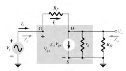
183 Ac equivalent model

184 Input and output impedances Voltage gain
185 Numerical For the above said configuration, the following results were got. K=0.24X10⁻³ A/V 2, V gsq =6.4V, I DQ =2.75mA. Determine gm, rd, Z i with and without the effect of rd, Z o with and without the effect of rd. Av with and without effect of rd. And compare the results. Id(sat)=6mA, VGS(th)=3V, VGS(on)=6V,yos=20uS. R D =2K ohms R F =10M ohms C1,c2=1uF Solution. gm=2k(v GS -V GS(th) ) =1.63mS. rd=1/yos=50kω Zi with rd: Rf ( rd // RD) Zi 1 gm( rd // RD)
186 = 2.42MΩ Zi without effect of rd: = 2.53MΩ Zo with rd: (R F parallel r d parallel R D ) = 1.92KΩ Zo without rd: Zo=RD = 2KΩ Gain A V with r d : = Without effect of rd: = RF Zi 1 gmr D
187 E MOSFET voltage divider configuration Important Parameters
188 Ac equivalent circuit
189 CHAPTER.6 :TRANSISTOR FREQUENCY RESPONSE To understand Decibels, log scale, general frequency considerations of an amplifier. low frequency analysis - Bode plot low frequency response BJT amplifier Miller effect capacitance high frequency response BJT amplifier Introduction It is required to investigate the frequency effects introduced by the larger capacitive elements of the network at low frequencies and the smaller capacitive elements of the active device at high frequencies. Since the analysis will extend through a wide frequency range, the logarithmic scale will be used. Logarithms To say that log a M = x means exactly the same thing as saying ax = M. For example: What is log 2 8? Basic Rules Logarithmic Rule 1: Logarithmic Rule 2: "To what power should 2 be raised in order to get 8?" Since 8 is 2 3 the answer is "3." So log 2 8 = 3 Logarithmic Rule 3: 1
190 Natural Logarithm (or base e) There is another logarithm that is also useful (and in fact more common in natural processes). Many natural phenomenon are seen to exhibit changes that are either exponentially decaying (radioactive decay for instance) or exponentially increasing (population growth for example). These exponentially changing functions are written as ea, where a represents the rate of the exponential change. In such cases where exponential changes are involved, we usually use another kind of logarithm called natural logarithm. The natural log can be thought of as Logarithm Base-e. This logarithm is labeled with ln (for "natural log"), where, e = Semi Log graph Decibels The term decibel has its origin in the fact that the power and audio levels are related on a logarithmic basis. The term bel is derived from the surname of Alexander Graham Bell. Bel is defined by the following equation relating two power levels, P1 and P2: G = [log 10 P2 / P1] bel It was found that, the Bel was too large a unit of measurement for the practical purposes, so the decibel (db) is defined such that 10 decibels = 1 bel. Therefore, GdB = [10 log 10 P2 / P1 ] db 2
191 The decimal rating is a measure of the difference in magnitude between two power levels. For a specified output power P2, there must be a reference power level P1. The reference level is generally accepted to be 1mW. GdBm = [10 log 10 P2 / 1mW ] dbm GdB = [10 log 10 P2 / P1 ] db = [10 log 10 (V 22 / R i ) / (V 12 / R i )] db = 10 log 10 (V 2 / V 1 )2 GdB = [20 log 10 V 2 / V 1 ] db One of the advantages of the logarithmic relationship is the manner in which it can be applied to cascaded stages wherein the overall voltage gain of a cascaded system is the sum of individual gains in db. Problem1: A V = (A v 1)(A v 2)(A v 3). A V db = (A v 1dB)+(A v 2dB)+(A v 3dB). Find the magnitude gain corresponding to a voltage gain of 100dB. Problem 2: GdB = [20 log 10 V 2 / V 1 ] db = 100dB = 20 log 10 V 2 / V 1 ; V 2 / V 1 = 10 5 = 100,000 The input power to a device is 10,000W at a voltage of 1000V. The output power is 500W and the output impedance is 20. Find the power gain in decibels. Find the voltage gain in decibels. GdB = 10 log 10 (P o /P i ) = 10 log 10 (500/10k) = dB GV = 20 log 10 (V o /V i ) = 20 log 10 (PR/1000) = 20 log 10 [(500)(20)/1000] = - 20dB ( Note: P = V 2 /R; V = PR) 3
192 Problem 3 : An amplifier rated at 40 W output is connected to a 10 speaker. a. Calculate the input power required for full power output if the power gain is 25dB. b. Calculate the input voltage for rated output if the amplifier voltage gain is 40dB. a. 25 = 10 log 10 40/P i P i = 40 / antilog(2.5) = 126.5mW b. GV = 20log 10 V o /V i ; Also, Thus, 40 = 20log 10 V o /V i V o /V i = antilog 2 = 100 V o = PR = (40)(10) = 20V V i = V o / 100 = 20/100 = 200mV General Frequency considerations At low frequencies the coupling and bypass capacitors can no longer be replaced by the short circuit approximation because of the increase in reactance of these elements. The frequency dependent parameters of the small signal equivalent circuits and the stray capacitive elements associated with the active device and the network will limit the high frequency response of the system. An increase in the number of stages of a cascaded system will also limit both the high and low frequency response. The horizontal scale of frequency response curve is a logarithmic scale to permit a plot extending from the low to the high frequency For the RC coupled amplifier, the drop at low frequencies is due to the increasing reactance of C C and C E, whereas its upper frequency limit is determined by either the parasitic capacitive elements of the network or the frequency dependence of the gain of the active device. In the frequency response, there is a band of frequencies in which the magnitude of the gain is either equal or relatively close to the midband value. To fix the frequency boundaries of relatively high gain, 0.707A Vmid is chosen to be the gain at the cutoff levels. 4
193 The corresponding frequencies f 1 and f 2 are generally called corner, cutoff, band, break, or half power frequencies. The multiplier is chosen because at this level the output power is half the midband power output, that is, at mid frequencies, P O mid = Vo 2 / Ro = A Vmid V i 2 / R O And at the half power frequencies, P OHPF = A Vmid V i 2 / R o = 0.5 A Vmid V i 2 / R o And, P OHPF = 0.5 P Omid The bandwidth of each system is determined by f 2 f 1 A decibel plot can be obtained by applying the equation, (A V / A Vmid )db = 20 log 10 (A V / A Vmid ) Most amplifiers introduce a 180 phase shift between input and output signals. At low frequencies, there is a phase shift such that V o lags V i by an increased angle. At high frequencies, the phase shift drops below 180. Low frequency analysis Bode plot In the low frequency region of the single stage BJT amplifier, it is the RC combinations formed by the network capacitors C C and C E, the network resistive parameters that determine the cutoff frequencies. Frequency analysis of an RC network 5
194 Analysis of the above circuit indicates that, X C = 1/2fC 0 Thus, V o = V i at high frequencies. At f = 0 Hz, X C =, V o = 0V. Between the two extremes, the ratio, A V = Vo / Vi will vary. As frequency increases, the capacitive reactance decreases and more of the input voltage appears across the output terminals. The output and input voltages are related by the voltage divider rule: the magnitude of V o = RV i / ( R jx C ) V o = RV i / R 2 + X C2 For the special case where X C = R, V o =RV i / R2 = (1/2) V i A V = V o / V i = (1/2) = The frequency at which this occurs is determined from, where, X C = 1/2f 1 C = R f 1 = 1/ 2RC Gain equation is written as, A V = V o / V i = R / (R jx C ) = 1/ ( 1 j(1/cr) = 1 / [ 1 j(f 1 / f)] In the magnitude and phase form, A V = V o / V i = [1 / 1 + (f 1 /f) 2 ] tan - 1 (f 1 / f) In the logarithmic form, the gain in db is 6
195 A V = V o / V i = [1 / 1 + (f 1 /f) 2 ] = 20 log 10 [1 / 1 + (f 1 /f) 2 ] = - 20 log 10 [ 1 + (f 1 /f) 2 ] = - 10 log 10 [1 + (f 1 /f) 2 ] For frequencies where f << f 1 or (f 1 / f) 2 the equation can be approximated by A V (db) = - 10 log 10 [ (f 1 / f) 2 ] = - 20 log 10 [ (f 1 / f)] at f << f 1 At f = f 1 ; f 1 / f = 1 and At f = ½ f 1 ; At f = ¼ f 1 ; At f = 1/10 f 1 ; 20 log 10 1 = 0 db f 1 / f = 2 20 log 10 2 = - 6 db f 1 / f = 4 20 log 10 2 = - 12 db f 1 / f = log = - 20dB The above points can be plotted which forms the Bode plot. Note that, these results in a straight line when plotted in a logarithmic scale. Although the above calculation shows at f = f 1, gain is 3dB, we know that f 1 is that frequency at which the gain falls by 3dB. Taking this point, the plot differs from the straight line and gradually approaches to 0dB by f = 10f 1. Observations from the above calculations: When there is an octave change in frequency from f 1 / 2 to f 1, there exists corresponding change in gain by 6dB. When there is an decade change in frequency from f 1 / 10 to f 1, there exists corresponding change in gain by 20 db. 7

196 Low frequency response BJT amplifier A voltage divider BJT bias configuration with load is considered for this analysis. For such a network of voltage divider bias, the capacitors C S, C C and C E will determine the low frequency response. Let us consider the effect of each capacitor independently. C S : f Ls 1 2 (Rs Ri)C Ri R1 R2 βre At mid or high frequencies, the reactance of the capacitor will be sufficiently small to permit a short circuit approximations for the element. The voltage V i will then be related to V s by V i mid = V s R i / (R i +R s ) s At f = F LS, V i = 70.7% of its mid band value. 8
 Effect of C C : Since the coupling capacitor is normally connected between the output of the")
Cc 1 Rs β fle Re RE ( re) 2πReCE Rs Rs R1 R2 9")
197 The voltage V i applied to the input of the active device can be calculated using the voltage divider rule: V i = R i V s / ( R i + R s jx Cs ) Effect of C C : Since the coupling capacitor is normally connected between the output of the active device and applied load, the RC configuration that determines the low cutoff frequency due to C C appears as in the figure given below. R o = R c r o Effect of C E : f LC 1 2π(Ro R L )Cc 1 Rs β fle Re RE ( re) 2πReCE Rs Rs R1 R2 9
198 The effect of C E on the gain is best described in a quantitative manner by recalling that the gain for the amplifier without bypassing the emitter resistor is given by: A V = - R C / ( r e + R E ) Maximum gain is obviously available where R E is 0. At low frequencies, with the bypass capacitor C E in its open circuit equivalent state, all of R E appears in the gain equation above, resulting in minimum gain. As the frequency increases, the reactance of the capacitor C E will decrease, reducing the parallel impedance of R E and C E until the resistor R E is effectively shorted out by C E. The result is a maximum or midband gain determined by A V = - R C / r e. The input and output coupling capacitors, emitter bypass capacitor will affect only the low frequency response. At the mid band frequency level, the short circuit equivalents for these capacitors can be inserted. Although each will affect the gain in a similar frequency range, the highest low frequency cutoff determined by each of the three capacitors will have the greatest impact. Problem: Determine the lower cutoff freq. for the network shown using the following parameters: C s = 10μF, C E = 20μF, C c = 1μF R s = 1kΩ, R 1 = 40kΩ, R 2 = 10kΩ, R E = 2kΩ, R C = 4kΩ, R L = 2.2kΩ, β = 100, r o = Ω, Vcc = 20V Solution: 10
199 a. To determine r e for the dc conditions, let us check whether R E > 10R 2 Here, R E = 200k, 10R 2 = 100k. The condition is satisfied. Thus approximate analysis can be carried out to find I E and thus r e. Mid band gain: Input impedance V B = R 2 V CC / ( R 1 +R 2 ) = 4V V E = V B 0.7 = 3.3V I E = 3.3V / 2k = 1.65mA r e = 26mV / 1.65mA = A V = V o / V i = -R C R L / r e = - 90 Zi = R1 R2 re = 1.32K Cut off frequency due to input coupling capacitor ( f Ls ) Effect of C E : f Ls = 1/ [2(R s +R i )C C1 = 6.86Hz. f Lc = 1 / [2(R C + R L ) C C = 1 / [ 6.28 (4k + 2.2k)1uF] = Hz R S = R S R 1 R 2 = R e = R E (R S / + r e ) = f Le = 1/2 R e C E = 327 Hz f Le = 327 Hz f LC = 25.68Hz f Ls = 6.86Hz In this case, f Le is the lower cutoff frequency. In the high frequency region, the capacitive elements of importance are the interelectrode ( between terminals) capacitances internal to the active device and the wiring capacitance between leads of the network. The large capacitors of the network that controlled the low frequency response are all replaced by their short circuit equivalent due to their very low reactance level. For inverting amplifiers, the input and output capacitance is increased by a capacitance level sensitive to the inter-electrode capacitance between the input and output terminals of the device and the gain of the amplifier. 11

200 Miller Effect Capacitance Any P-N junction can develop capacitance. This was mentioned in the chapter on diodes. In a BJT amplifier this capacitance becomes noticeable between: the Base- Collector junction at high frequencies in CE BJT amplifier configurations. It is called the Miller Capacitance. It effects the input and output circuits. I i = I 1 + I 2 Eqn (1) Using Ohm s law yields and I 1 = V i / Z i, I 1 = V i / R 1 I 2 = (V i V o ) / X cf = ( V i A v V i ) / X cf I 2 = V i (1 A v ) / X cf Substituting for I i, I 1 and I 2 in eqn(1), V i / Z i = V i / R i + [(1 A v )V i ] /X cf 1/ Z i = 1/R i + [(1 A v )] /X cf 1/ Z i = 1/R i + 1/ [X cf / (1 A v )] 1/ Z i = 1/R i + 1/ X CM Where, X CM = [X cf / (1 A v )] = 1/[ (1 A v ) C f ] C Mi = (1 A v ) C f C Mi is the Miller effect capacitance. 12

201 For any inverting amplifier, the input capacitance will be increased by a Miller effect capacitance sensitive to the gain of the amplifier and the inter-electrode ( parasitic) capacitance between the input and output terminals of the active device. Miller Output Capacitance (C Mo ) Applying KCL at the output node results in: and I o = I 1 +I 2 I 1 = V o /R o I 2 = (V o V i ) / X Cf The resistance R o is usually sufficiently large to permit ignoring the first term of the equation, thus Substituting V i = V o / A V, C I o (V o V i ) / X Cf I o = (V o V o /A v ) / X Cf Mo Cf = V o ( 1 1/A V ) / X Cf I o / V o = (1 1/A V ) / X Cf V o / I o = X Cf / (1 1/A V ) = 1 / Cf (1 1/A V ) = 1/ C Mo C Mo = ( 1 1/A V )C f 13
202 C Mo C f [ A V >>1] If the gain (A v ) is considerably greater than 1: High frequency response BJT Amplifier At the high frequency end, there are two factors that define the 3dB cutoff point: The network capacitance ( parasitic and introduced) and the frequency dependence of h fe () Network parameters In the high frequency region, the RC network of the amplifier has the configuration shown below. o Vi C At increasing frequencies, the reactance X C will decrease in magnitude, resulting in a short effect across the output and a decreased gain. V o = V i (-jx C ) / R -jx C V o / V i = 1/[ 1+j(R/X C )] ; X C = 1/2fC A V = 1/[ 1+j(2fRC)]; A V = 1/[ 1+jf/f 2 ] Mo Cf This results in a magnitude plot that drops off at 6dB / octave with increasing frequency. Vo 14
203 Network with the capacitors that affect the high frequency response Capacitances that will affect the high-frequency response: C be, C bc, C ce internal capacitances C wi, C wo wiring capacitances C S, C C coupling capacitors C E bypass capacitor The capacitors C S, C C, and C E are absent in the high frequency equivalent of the BJT amplifier.the capacitance C i includes the input wiring capacitance, the transition capacitance C be, and the Miller capacitance C Mi.The capacitance C o includes the output wiring capacitance C wo, the parasitic capacitance C ce, and the output Miller capacitance C Mo.In general, the capacitance C be is the largest of the parasitic capacitances, with C ce the smallest. As per the equivalent circuit, f H = 1 / 2R thi C i R thi = R s R 1 R 2 R i C i = C wi +C be +C Mi = C Wi + C be +(1- A V ) C be 15
204 At very high frequencies, the effect of C i is to reduce the total impedance of the parallel combination of R 1, R 2, R i, and C i.the result is a reduced level of voltage across C i, a reduction in I b and the gain of the system. For the output network, f Ho = 1/(2R Tho C o ) R Tho = R C R L r o C o = C wo +C ce +C Mo At very high frequencies, the capacitive reactance of C o will decrease and consequently reduce the total impedance of the output parallel branches. The net result is that V o will also decline toward zero as the reactance X c becomes smaller.the frequencies f Hi and f Ho will each define a -6dB/octave asymtote. If the parasitic capacitors were the only elements to determine the high cutoff frequency, the lowest frequency would be the determining factor.however, the decrease in h fe (or ) with frequency must also be considered as to whether its break frequency is lower than f Hi or f Ho. hfe (or ) variation The variation of h fe ( or ) with frequency will approach the following relationship h fe = h fe mid / [1+(f/f )] f is that frequency at which h fe of the transistor falls by 3dB with respect to its mid band value. The quantity f is determined by a set of parameters employed in the hybrid model. In the hybrid model, r b includes the base contact resistance base bulk resistance base spreading resistance 16
205 Hybrid model The resistance r u (r bc ) is a result of the fact that the base current is somewhat sensitive to the collector to base voltage. Since the base to emitter voltage is linearly related to the base current through Ohm s law and the output voltage is equal to the difference between the base the base to emitter voltage and collector to base voltage, we can say that the base current is sensitive to the changes in output voltage. Thus, Therefore, f = 1/[2r (C +C u )] r = r e = h fe mid r e f = 1/[2 h femid r e (C +C u )] OR f = 1/[2 mid r e (C +C u )] The above equation shows that, f is a function of the bias configuration. As the frequency of operation increases, h fe will drop off from its mid band value with a 6dB / octave slope. Common base configuration displays improved high frequency characteristics over the common emitter configuration. Miller effect capacitance is absent in the Common base configuration due to non inverting characteristics. A quantity called the gain bandwidth product is defined for the transistor by the condition, h femid / [1+j(f/f ) = 1 So that, h fe db = 20 log 10 h femid / [1+j(f/f ) = 20 log 10 1 = 0 db The frequency at which h fe db = 0 db is indicated by f T. 17
206 h femid / [1+j(f/f ) = 1 h femid / 1+ (f T /f ) 2 h femid / (f T /f ) =1 ( by considering f T >>f ) Thus, f T = h femid f OR f T = mid f But, f = 1/[2 mid r e (C +C u )] f T = ( mid ) 1/[2 mid r e (C +C u )] Problem: f T = 1/[2 r e (C +C u )] For the amplifier with voltage divider bias, the following parameters are given: R S = 1k, R 1 = 40k, R 2 = 10k, R c = 4k, R L = 10k C s = 10F, C c = 1 F, C E = 20 F = 100, r o =, V CC = 10 C = 36pF, C u = 4pF, C ce =1pF, C wi =6pF, C wo =8pF a. Determine f Hi and f Ho b. Find f and f T Solution: To find r e, DC analysis has to be performed to find I E. V B = R 2 V CC / R 1 +R 2 = 2V V E = = 1.3V I E = 1.3/1.2K = 1.083mA r e = 26mV / 1.083mA r e = 24.01, r e = 2.4k R i = R S R 1 R 2 r e R i = 1.85k A V = V o /V i = - (R c R L ) / r e A V = R Thi = R s R 1 R 2 R i 18
207 R Thi = 0.6k To determine f Hi and f Ho : f Hi = 1/[2R Thi C i ] ; C i = C wi +C be +(1 A V )C bc = 6pF + 36pF + (1 (-119)) 4pF C i = 522pF f Hi = 1/2R Thi C i f Hi = kHz R Tho = R c R L R Tho = 2.86k C o = C wo +C ce +C Mo = 8pF+1pF+(1 (1/-119))4pF C o = 13.03pF f Ho = 1/2R Tho C o f Ho = 8.542MHz f = 1/[2 mid r e (C +C u )] f = 1.66MHz f T = f f T = MHz Summary Frequency response of BJT Amplifiers Logarithm of a number gives the power to which the base must be brought to obtain the same number Since the decibel rating of any equipment is a comparison between levels, a reference level must be selected for each area of application. For Audio system, reference level is 1mW The db gain of a cascaded systems is the sum of db gains of each stage. It is the capacitive elements of a network that determine the bandwidth of a system. The larger capacitive elements of the design determine the lower cutoff frequencies. Smaller parasitic capacitors determine the high cutoff frequencies. The frequencies at which the gain drops to 70.7% of the mid band value are called cutoff, corner, band, break or half power frequencies. The narrower the bandwidth, the smaller is the range of frequencies that will permit a transfer of power to the load that is atleast 50% of the midband level. 19
208 A change in frequency by a factor of 2, is equivalent to one octave which results in a 6dB change in gain. For a 10:1 change in frequency is equivalent to one decade results in a 20dB change in gain. For any inverting amplifier, the input capacitance will be increased by a Miller effect capacitance determined by the gain of the amplifier and the inter electrode ( parasitic) capacitance between the input and output terminals of the active device. C Mi = (1 A V )C f Also, C Mo C f (if A V >>1) A 3dB drop in will occur at a frequency defined by f, that is sensitive to the DC operating conditions of the transistor. This variation in defines the upper cutoff frequency of the design. Problems: 1. The total decibel gain of a 3 stage system is 120dB. Determine the db gain of each stage, if the second stage has twice the decibel gain of the first and the third has 2.7 times decibel gain of the first. Also, determine the voltage gain of the each stage. Given: G dbt = 120dB We have Given, Therefore, G dbt = G db1 +G db2 +G db3 G db2 = 2G db1 G db3 = 2.7G db1 120dB = 5.7G db1 G db1 = 21.05, G db2 = G db3 =56.84 We have G db = 10 log[v o / V i ] V o / V i = antilog ( G db /10) G1 = G2 = 16.21k G3 = k 2. If the applied ac power to a system is 5W at 100mV and the output power is 48W, determine a. The power gain in decibels 20
209 b. The output voltage c. The voltage gain in decibels, if the output impedance is 40k. d. The input impedance Given: P i = 5W.V i = 100mV, P o = 48w R o = 40k a. G db =10 log [48/ 5] = b. P o = V o 2 /R o, V o = P o R o = V c. Voltage gain in db = 20 log [ /100m] = d. R i = V i 2 / P i = 2k General steps to solve a given problem: Normally, the amplifier circuit with all the values of biasing resistors, value of and values inter electrode capacitances ( C be, C bc and C ce ) will be given. It is required to calculate: f LS, f LC and f LE Also, f Hi, f Ho, f and f T Step1: Perform DC analysis and find the value of I E, and r e Find the value of R i ( Z i ) using the value of r e Find the value of A Vmid Step 2: Find f LS using the formula 1/2(R i +R S )C S Step 3: Find f LC using the formula 1/2(R C +R L )C C Step 4: Determine the value of f LE using the formula 1/2R e C E where, R e = R E [(R S )/ + r e ] R S = R S R 1 R 2 Step 5: Determine f Hi using the formula 1/2R Thi C i where R Thi = R 1 R 2 R S r e C i = C wi + C be + (1-A V )C bc Step 6: Determine f Ho using the formula 1/2R Tho C o where R Tho = R C R L r o C o = C wo + C ce + C bc Step 7: Determine f using the formula 1/[2 mid r e (C +C u )] 21
210 Step 8: Determine f T using the formula f T = mid f Problem: Determine the following for the given network: 1. f Ls 2. f Lc 3. f LE 4. f Hi 5. f Ho 6. f and f T Given: Solution: V CC = 20V, R B = 470k, R C = 3k, R E = 0.91k, R S = 0.6k, R L = 4.7k C S = C C = 1F, C E = 6.8 F C wi = 7pF, C wo =11pF, C be = 6pF, C be = 20pF and C ce = 10pF I B = (V CC V BE ) / [R B + ( +1)R E ] I B = 3.434mA I E = I B I E = 3.434mA r e = 26mV / I E r e =
211 A V = - (R C R L ) / r e A V = where, Z i = R B r e Z i = f LS = 1/2(R i +R S )C S f LS = Hz f LC = 1/2(R C +R L )C C f LC = Hz f LE = 1/2R e C E ; R e = [(R S /)+ r e ] R E R S = R B R S f LE = 1.752kHz C i = C wi + C be + (1 A V ) C bc C i = 1.48nF R Thi = R S R B r e R Thi = f Hi = 1 / 2(1.48nF)(334.37) f Hi = KHz C o = C Wo + C ce + (1 1/A V ) C bc C o = 27.02pF R Tho = R C R L R Tho = 1.83K f Ho = 1 / 2(27.02p)(1.83k) f Ho = 3.21MHz f = 1 / 2 (100) (7.56)( 20p + 6p) f = 8.09MHz f T = f f T = 803MHz 23
212 Equations - Logarithms 1. a = bx, x = log b a 2. G db = 10 log P 2 / P 1 3. G db = 20 log V 2 / V 1 Equations Low frequency response 1. A V = 1 / [1 j(f 1 /f)], where, f 1 = 1/2RC Equations BJT low frequency response 1. f Ls = 1 / [2(R S +R i )C S ], where, R i = R 1 R 2 r e 2. f LC = 1 /[2(R o +R L )C C ], where, R o = R C r o 3. f LE = 1 / 2R e C E, where, R e = R E ( R S / +r e ) and R S = R S R 1 R 2 Miller effect Capacitance C Mi = (1 A V )C f, C MO = ( 1 1/A V )C f BJT High frequency response: 1. A V = 1/ [1 + j(f/f 2 )] 2. f Hi = 1 / 2R Thi C i, where, R Thi = R S R 1 R 2 R i, C i = C Wi +C be + C Mi 3. f HO = 1/ 2R Tho C o, where, R Tho = R C R L r o C o = C Wo +C ce + C Mo 4. f = 1/[2 mid r e (C +C u )] 5. f T = f 24
213 Introduction Definitions and amplifier types Series fed class A amplifiers Analog Electronics Circuits Power Amplifiers Transformer coupled class A amplifier Transformer coupled amplifier continuation Numerical Class B amplifier operation Class B amplifier circuits Numerical Amplifier distortion Numerical Second harmonic distortion Power transistor heat sinking Thermal analogy of power transistor Class C and class D amplifiers Numerical
214 Introduction Amplifier receives a signal from some pickup transducer or other input source and provides larger version of the signal. In small signal amplifiers the main factors are usually amplification, linearity and magnitude of gain. Classes of PAs Amplifier classes represent the amount the output signal varies over one cycle of operation for a full cycle of input signal So the following classes of PA are defined Class A Class B Class AB Class C Class D Class A amplifier Class A amplifying devices operate over the whole of the input cycle such that the output signal is an exact scaled-up replica of the input with no clipping. Class A amplifiers are the usual means of implementing smallsignal amplifiers. They are not very efficient. a theoretical maximum of 50% is obtainable with inductive output coupling and only 25% with capacitive coupling. In a Class A circuit, the amplifying element is biased so the device is always conducting to some extent, and is operated over the most linear portion of its characteristic curve Because the device is always conducting, even if there is no input at all, power is drawn from the power supply. This is the chief reason for its inefficiency.
215 Class B Class B amplifiers only amplify half of the input wave cycle. As such they create a large amount of distortion, but their efficiency is greatly improved and is much better than Class A. Class B has a maximum theoretical efficiency of 78.5% (i.e., π/4). This is because the amplifying element is switched off altogether half of the time, and so cannot dissipate power. A single Class B element is rarely found in practice, though it can be used in RF power amplifier where the distortion levels are less important. However Class C is more commonly used for this.
216 Class AB A practical circuit using Class B elements is the complementary pair or "push pull" arrangement. Here, complementary or quasi-complementary devices are used to each amplify the opposite halves of the input signal, which is then recombined at the output. This arrangement gives excellent efficiency, but can suffer from the drawback that there is a small mismatch at the "joins" between the two halves of the signal.. Class AB sacrifices some efficiency over class B in favor of linearity, so will always be less efficient (below 78.5%). It is typically much more efficient than class A.
217 Class C Class C amplifiers conduct less than 50% of the input signal and the distortion at the output is high, but high efficiencies (up to 90%) are possible. Some applications (for example, megaphones) can tolerate the distortion. A much more common application for Class C amplifiers is in RF transmitters, where the distortion can be vastly reduced by using tuned loads on the amplifier stage. The input signal is used to roughly switch the amplifying device on and off, which causes pulses of current to flow through a tuned circuit.
218 Class D Class D amplifiers are much more efficient than Class AB power amplifiers. As such, Class D amplifiers do not need large transformers and heavy heatsinks, which means that they are smaller and lighter in weight than an equivalent Class AB amplifier. All power devices in a Class D amplifier are operated in on/off mode. These amplifiers use pulse width modulation,

219 Comparison of Amplifier classes Series fed class A amplifiers It is a fixed bias circuit.

220 DC bias operation The DC bias set by Vcc and Rb Collector current I C =βi B Collector emitter voltage V CE =V CC -I C R C Load line Power considerations The power into an amplifier is provided by the power supply With no input supply, current drawn is collector bias current I Cq. pi(dc)=v CC I Cq Output power The output voltage and current varying around the bias point provide ac power to the load. I B Vcc 0.7V RB
221 Using rms signals P 0 (ac)=v CE (rms)i C (rms) =I 2 C(rms) Rc =V 2 C(rms)/Rc Using peak signals The ac power delivered to the load is p 0 ={V CE (p) I C (p)} / 2 or = {I 2 c(p)/2} Rc ={V 2 CE(p)}/2Rc Using peak-peak signals P 0 (ac)={v CE (p-p) I C (p-p)}/8 Efficiency = {I 2 c(p-p)/8} Rc ={V 2 CE(p)}/8Rc Efficiency of an amplifier represents the amount of ac power delivered from dc source. It can be calculated using Po( ac) Pi( dc) % x Maximum Efficiency Maximum voltage swing V CE (p-p)=v CC Maximum current swing I C (p-p)=v CC /R C Maximum power 100 Vcc( Vcc / Rc) Po( ac) 8 The maximum power input evaluated using dc bias current set to half of the maximum value.
222 Maximum Pi(dc)=V CC (maximum I C ) Maximum efficiency = {maximum Po(ac)/ Maximum efficiency maximum Pi(dc)} x100 = 25% The maximum efficiency of a class A series fed amplifier is thus seen to be 25%. The maximum efficiency occurs only for ideal conditions of both voltage Numerical and current swing.thus practical circuits will have less than this percentage. Calculate input power, output power and efficiency of the amplifier circuit for the circuit shown below for an input voltage that increases the base current by 10mA peak. Data given VCC=20V Rc=20 ohms RB=1k ohms β=25 Vcc / Rc Vcc 2 2 V cc / 8Rc x100 2 V cc / 2Rc
223 Solution Hint: use the above derived formulae Po(ac)=0.625W Pi(dc)=9.6W Efficiency=6.5%
224 Transformer coupled class A amplifier The transformer can step up or step down a voltage applied to primary coil. Transformer coupled class A PA A form of class A amplifier having maximum efficiency of 50% uses transformer to couple the output signal to the load. Impedance transformation If α=n1/n2 Then Above equation reduces to N N V V N N I I / 2 2 / 1 2 N N N N N N I I I V I V I V R R RL RL N N R R RL RL
225 Load resistance reflected to the primary side as, R1 OR RL Transformer coupled amplifier R2 RL Drawing DC and AC load line Signal swing and output AC power V I CE( p p) C ( p p) P o( ac) V L V V I 1 C max Power across the load can be expressed as I L =I 2 =N 1 /N 2 I C with the output ac power then calculated using P L =I 2 L (rms) R L 2 CE max 2 I V C min CE min ( VCE max VCE min C max IC min N 2 2 V1 N1 P L V L( rms) R L )( I 8 )
226 Numerical Calculate the ac power delivered to 8 ohm speaker for the circuit shown below. The circuit component values result in a dc base current of 6mA, and the input signal Vi results in a peak base current swing of 4mA. Solution: Step 1: dc load line is drawn vertically from voltage point V CEQ =V CC =10V Step 2: for IB=6mA the operating point V CEQ =10V & I CQ =140mA Step 3: the effective resistance seen at the primary is R L =(N1/N2) 2 R L =72 ohms. Step 4: the ac load line can be drawn of slope 1/72. I C =V CE /R L =10/72=139mA Mark point A on graph.. I CEQ +I C =140mA+139mA Connect point A through the point Q to obtain the ac load line.
227 For a given base current of 4mA peak, the maximum and minimum collector current and collector emitter voltage obtained from graph.. Efficiency The input dc power obtained from the supply is calculated from the supply dc voltage and thus average power drawn from the supply P i (dc)= V CC I CQ For the transformer coupled amplifier power dissipated by the transformer is small (due to small resistance) The only power loss considered here is that dissipated by the power transistor and calculated by P ( V ac) P Q =P i (dc) - P o (ac) V Maximum theoretical efficiency )( I CE max CE min C max C min o( 8 I ( )(255m 25m) P o ( ac) W 8 Po( ac) Pi( dc) % x 100 ( VCE maxvce min) % 50 ( VCE maxvce min) 2 % )
228 Larger the value of VCEmax and smaller the value of VCEmin, the closer the efficiency approaches the theoretical limit of 50% Numerical Calculate the efficiency of a transformer coupled class A amplifier for a supply of 12V and outputs of : a. V(p)=12V b. V(p)=6V c. V(p)=2V Solution : Here V CE =V CC =12V, the maximum and minimum of the voltage swing are V CEmax =V CEQ +V(p)=12V+12V=24V VCEmin=VCEQ-V(p)=12V-12V=0V This results in efficiency of, Case ii % % V CEmax =V CEQ +V(p)=12V+6V=18V VCEmin=VCEQ-V(p)=12V-6V=6V This results in efficiency of 12.5% Case iii. V CEmax =V CEQ +V(p)=12V+2V=14V VCEmin=VCEQ-V(p)=12V-2V=10V This results in efficiency of 1.39% 2

229 Class B Amplifier operation Class B operation is provided when the dc bias leaves the transistor biased just off, the transistor turning on when the ac signal is applied. This is essentially no bias and conducts for only one half cycle. To obtain output for full cycle, it is required to use two transistors and have each conduct on opposite half-cycles, the combined operation providing a full cycle of output on opposite half cycles of output signal. Since one part of the circuit pushes the signal high during one half cycle and other part pulls the signal low during the other half cycle, the circuit is referred to as push-pull circuit. Class B operation provides greater efficiency than was possible using single transistor in class A operation. Class B push-pull
230 Power equations Input DC power Pi(dc)=V CC I dc Here Idc is the average current drawn Hence Idc can be written as Hence input power is equal to Output ac power can be evaluated as, Efficiency: 2 Pi( dc) Vcc I( p) V P ( ac) Po( ac) Pi( dc) % x % 4 o 2 2 L ( rms) R L 100 VL ( p) / 2RL x100% V [(2 / ) I( p)] CC VL( p) x % Vcc 2 I( p) Idc
231 Power dissipated by output transistors P 2Q =P i (dc)-p o (ac) Power handled by each transistor =P 2Q /2 Numerical: For a class B amplifier providing a 20V peak signal to a load of 16 ohms (speaker) and power supply of VCC=30V, determine the input power, output power, and circuit efficiency. Solution: Hint : use the above derived formulae Pi(dc)=23.9W Po(ac)=12.5W Efficiency=52.3% For a class B amplifier using supply of VCC=30V and driving a load of 16ohms determine the maximum input power, output power and transistor dissipation. Solution: Hint : use the above derived formulae Po(ac)=28.125W Pi(dc)=35.81W Efficiency=78.54% Pq=5.7W
232 Efficiency in another form Numerical 1. Calculate the efficiency of a class B amplifier for a supply voltage of VCC=24V with peak output voltages of a. VL(p)=22V b. VL(p)=6V VL ( p) Po( ac) 2R 2 L 2V ( p) L Pi( dc) VCCI dc VCC RL VL2( p) / 2RL % x100 2V L ( p) VCC R L VL( p) % % Vcc
233 Class B amplifier circuits To obtain phase inverted signals. To use transformers using op-amps Using transistors Phase splitter circuits Using BJT
234 Using op-amp Transformer coupled push-pull amplifier
235 Complementary symmetry circuits Working of the circuit Every transistor will conduct for half cycle Single input signal is applied to the base of both transistors npn transistor will be biased in conduction for positive half cycle of the input. During negative half cycle pnp transistor is biased into conduction when input goes to negative. Disadvantages One disadvantage is that the need of two separate voltage supplies. Cross over distortion in the output signal This cross over distortion is referred to as the nonlinearity in the output signal during cross over from positive to negative or vice-versa. This is due to the fact that, none of the transistors are on near zero input and thus output does not follow input.
236 Complementary symmetry push-pull circuit using Darlington transistors This circuit provides higher output current and lower output resistance. Here the load resistance is matched by low output resistance of the driving source. Quasi complementary push-pull transformer less power amplifier In practical circuit it is preferred to use npn for both high-current-output devices. Practical means of obtaining complementary operation while using same, matched transistors for the output is provided by a quasi complementary circuit.
237 Circuit Here push-pull operation is achieved by using complementary transistors(q1 and Q2) before the matched npn output transistors (Q3 and Q4) Q1 and Q3 forms a Darlington connection Q2 and Q4 forms a feedback connection, which similarly provides lowimpedance to drive the load. Resistor R2 can be adjusted to minimize cross over distortion by adjusting the dc bias condition. This is the most popular form of power amplifier used today.
238 Numerical For the circuit shown calculate input power, output power and power handled by each transistor and circuit efficiency. Given Vcc=+25V and VEE=-25V Input vi=12v Load resistance=4 ohms Solution: Hint: use the above derived formulae. Po(ac)=36.125W Pi(dc)=67.75W PQ=15.8W Efficiency=53.3%
239 Numerical For the circuit calculate maximum input power, maximum output power, input voltage for maximum power operation and power dissipated by the output transistor at this voltage. Solution: Hint: use the above derived formulae Pi(dc)=99.47W Po(ac)=78.125W Efficiency=78.54% To achieve maximum power operation the output voltage must be VL(p)=VCC PQ=21.3W Numerical For the circuit shown, determine the maximum power dissipated by the output transistors and the input voltage at which this occurs. Solution: PQ=31.66W VL=15.9V
240 Amplifier distortion Any signal varying over less than the full cycle is considered to have distortion. An ideal amplifier is capable of amplifying a pure sinusoidal signal to provide a larger version, the resulting waveform being a pure sinusoidal frequency sinusoidal signal. When distortion occurs, output will not be an exact duplicate of input signal (except for magnitude) Distortion can occur because the device characteristic is not linear. In this case non linear or amplitude distortion occurs. Distortion can also occur because the circuit elements and devices respond to the input signal differently at various frequencies, this being frequency distortion. One technique for describing distorted but period waveforms uses Fourier Example analysis, a method that describes any periodic waveform in terms of its fundamental frequency component and frequency components at integer multiples- these components are called harmonic components or harmonics. A fundamental frequency of 1KHz could result in harmonics of 2KHz,3KHz,4KHz so on., 1KHz is termed as fundamental frequency 2KHz is termed as second harmonic 3KHz is termed as third harmonic and so on.,
241 Harmonic Distortion A signal is considered to have harmonic distortion when there are harmonic frequency components. If fundamental frequency has amplitude A1, and n th frequency component has an amplitude of An. Harmonic distortion can be defined as % nth harmonic distortion= Numerical Calculate the harmonic distortion components for an output signal having fundamental amplitude of 2.5V, second harmonic amplitude of 0.1V, and fourth harmonic amplitude of 0.05V. Solution: % D % D % D A2 x100% A1 A3 x100% A1 A4 x100% A1 An % D x100% A x100% 10% x100% 4% x100% 2% 2.5
242 Total harmonic distortion When an output signal has a number of individual harmonic distortion components, the signal can be seen to have a total harmonic distortion based on the individual elements as combined by relation, Numerical Calculate the total harmonic distortion for the amplitude components given in previous example Solution: Second harmonic distortion I c =I CQ +I o +I 1 cos wt + I 2 cos wt I cq quiescent current I o additional dc current due to non zero average of the distorted signal % THD % THD % THD % THD 10.95% Solving for I1 and I2, D2 D3 D4... x100% I1 fundamental component of current D2 D3 D4... x100% second harmonic current due to twice the fundamental frequency 2... x100% Ic max Ic min 2Icq Io I2 4 Ic max Ic min I1 2
243 Definition of second harmonic can be Numerical In voltage terms An output waveform displayed on oscilloscope provides the following measurements, i.v CEmin =1V; V CEmax =22V;V CEQ =12V ii.v CEmin =4V;V CEmax =20V;V CEQ =12V solution: D2 1 2 V CE max V V CE max CE min V CE min V CEQ x100% 1 ( VCEMAX VCEMIN ) VCEQ D2 2 x100% V V i.. D2 CEMAX CEMIN i.. D x100% 2.38% x100% 0%( no distotion) 22 4
244 Power of signal having distortion Power delivered to the load resistor Rc due to the fundamental component of the distorted signal is Total power due to all the harmonic components of the distorted signal is, In terms of Total harmonic distortion P (1 D Numerical 2 2 P (1 THD For harmonic distortion reading of D2=0.1,D3=0.02 and D4=0.01, with I1=4A and Rc=8 ohms, calculate THD, fundamental power component and total power. Solution: THD=0.1 P1=64W P=64.64W P ( I D ) P I P1 I 2 1 c R 2 Rc...) 2 Graphical description of harmonic components of distorted signal ) I I All the components are obtained by Fourier analysis 2 1 Rc 2 Conclusion: any periodic signal can be represented by adding a fundamental component and all harmonic components varying in amplitude and at various phase angles. 2 3
245 Power transistor heat sinking Heat is produced in transistors due to the current flowing through them. If you find that a transistor is becoming too hot to touch it certainly needs a heat sink! The heat sink helps to dissipate (remove) the heat by transferring it to the surrounding air. Heat sink Maximum power handled by a particular device and the temperature of the transistor junction are related since the power dissipated causes an increase in temperature at the junction of the device. Example : a 100 W transistor will provide more power than 10 W transistor. Proper heat sinking techniques will allow operation of a device at about onehalf its maximum power rating. There are two types of bipolar transistors Germanium Junction temperature : C Silicon Junction temperature : C Silicon transistors provide greater maximum temperature Average power dissipated may be approximated by P D =V CE I C This power dissipation is allowed only up to a maximum temperature.
246 Above maximum temperature, device power dissipation must be reduced (derated) so that at higher temperature, power handling capacity is reduced. The limiting factor in power handling by a particular transistor is the temperature of the device s collector junction. Power transistors are mounted in large metal cases to provide a large area from which the heat generated by the device may radiate. Even then the device power rating limited. Instead if the device is mounted on the heat sink power handling capacity is increased. The derated curve for silicon transistor given by Mathematical definition. P ( temp1) P D D derating factor ( temp0) ( Temp1 Temp0) x
247 Numerical: Determine what maximum dissipation will be allowed for an 80W silicon transistor rated at 25 degree C. if derating s required above this temp by derating factor of 0.5W/degree C at case temp of 125 degree C. Solution: Using the above formula Power derated is 30W Thermal analogy of power transistor θja total thermal resistance (jn to ambient) θjc transistor thermal resistance (jn. To case) θcs insulator thermal resistance (case to heat-sink θsa heat-sink thermal resistance (heat sink to ambient) Usng electrcal analogy θja= θjc+ θcs + θsa This analogy can be used n applying kirchoff s law as TJ = PD θja +TA The thermal factor θ provides information about how much temp drop( or rise) for amount of power dissipation. Eg: θjc =0.5 deg C/W means that power dissipation of 50W.the dffernce between junton temp and case temp s gven by TJ-TC = θjc PD = 0.5x50 =25 deg C. Value of thermal resistance from junction to free air (using HS) 40 deg C/W For this thermal resistance only 1W of power dissipation results n junction temp 40 deg C greater than the ambient.
248 A HS can now be seen to provide a low thermal resistance between case and air much less than 40 deg C/W value of case alone. Using HS having θsa 2 deg C/W And insulating thermal resistance (case to HS) θcs 0. 8 deg C/W Finally for transistor θjc 0.5 deg C/W θja= θjc+ θcs + θsa = = 3.3 deg C/W With HS thermal resistance between air and the junction is only 3.3 deg C/W compared 40 deg C/W for transistor operating directly in to free air Numerical: A silicon power transistor s operated with a HS θsa = 1.5 deg C/w. the transistor rated at 150W(25 deg C) has θjc =0.5 deg C/W and the mounting insulation has θcs =0.6 deg C /W. what s the max power dissipated f the ambient temp s 40 deg C and TJ max s 200 deg C Solution : pd =(TJ-TA)/ θsa + θjc + θcs = 61.5W
249 Class C and Class D amplifiers Class C The circuit is biased to operate for less than 180 deg of input cycle. The tuned circuit n the load provide a full cycle of output signal for fundamental frequency of tuned LC circuit. This type of operation s thus limited to one fixed frequency as n communication systems. Not suitable for power amplification Class D amplifier Class D designed to operate with digital or pulse type signals Efficiency of 90% can be achieved. Desirable for power amplifiers. Necessary to convert any input signal in to pulse type wave before using to drive a large power load and to convert the signal back to sinusoidal type signal to recover the original signal.
250 Here class D amplifier we can also consider D stands for Digital since that s the name of the signal provided to the class D amplifier. Block diagram of class D Most of the power applied to the amplifier is transferred to the load the efficiency of the circuit s typically very high.

251 Chapter.8: Oscillators Objectives: To understand The basic operation of an Oscillator the working of low frequency oscillators RC phase shift oscillator Wien bridge Oscillator the working of tuned oscillator Colpitt s Oscillator, Hartley Oscillator Crystal Oscillator the working of UJT Oscillator Basic operation of an Oscillator An amplifier with positive feedback results in oscillations if the following conditions are satisfied: The loop gain ( product of the gain of the amplifier and the gain of the feedback network) is unity The total phase shift in the loop is 0 If the output signal is sinusoidal, such a circuit is referred to as sinusoidal oscillator. 1

252 When the switch at the amplifier input is open, there are no oscillations. Imagine that a voltage Vi is fed to the circuit and the switch is closed. This results in V o = A V Vi and V o = V f is fed back to the circuit. If we make V f = V i, then even if we remove the input voltage to the circuit, the output continues to exist. V o = A V V i V o = V f A V V i = V f If V f has to be same as V i, then from the above equation, it is clear that, A V =1. Thus in the above block diagram, by closing the switch and removing the input, we are able to get the oscillations at the output if A V =1, where A V is called the Loop gain. Positive feedback refers to the fact that the fed back signal is in phase with the input signal. This means that the signal experiences 0 phase shift while traveling in the loop. The above condition along with the unity loop gain needs to be satisfied to get the sustained oscillations. These conditions are referred to as Barkhausen criterion. Another way of seeing how the feedback circuit provides operation as an oscillator is obtained by noting the denominator in the basic equation A f = A / (1+A). When A = -1 or magnitude 1 at a phase angle of 180, the denominator becomes 0 and the gain with feedback A f becomes infinite.thus, an infinitesimal signal ( noise voltage) can provide a measurable output voltage, and the circuit acts as an oscillator even without an input signal. Phase shift oscillator The phase shift oscillator utilizes three RC circuits to provide 180º phase shift that when coupled with the 180º of the op-amp itself provides the necessary feedback to sustain oscillations. The gain must be at least 29 to maintain the oscillations. The frequency of resonance for the this type is similar to any RC circuit oscillator: f r = 1/26RC 2
 At the operating frequency, we can assume that the input impedance of the amplifier is infinite.")
253 FET phase shift oscillator The amplifier stage is self biased with a capacitor bypassed source resistor R s and a drain bias resistor R D. The FET device parameters of interest are gm and rd. A = g m R L, where R L = (R D r d / R D + r d ) At the operating frequency, we can assume that the input impedance of the amplifier is infinite. This is a valid approximation provided, the oscillator operating frequency is low enough so that FET capacitive impedances can be neglected. The output impedance of the amplifier stage given by R L should also be small compared to the impedance seen looking into the feedback network so that no attenuation due to loading occurs. RC Phase shift Oscillator - BJT version If a transistor is used as the active element of the amplifier stage, the output of the feedback network is loaded appreciably by the relatively low input resistance ( h ie ) of the transistor. 3
.")
254 An emitter follower input stage followed by a common emitter amplifier stage could be used.if a single transistor stage is desired, the use of voltage shunt feedback is more suitable. Here, the feedback signal is coupled through the feedback resistor R in series with the amplifier stage input resistance ( R i ). Problem: f = (1/2RC)[1/ 6 + 4(RC / R)] h fe > (R/RC) + 4 (RC / R) It is desired to design a phase shift oscillator using an FET having g m = 5000S, r d = 40 k, and a feedback circuit value of R = 10 k. Select the value of C for oscillator operation at 5 khz and R D for A > 29 to ensure oscillator action. Solution: f = 1/26RC ; C = 1/26Rf = 1.3nF A = g m R L Let A = 40; RL = A / gm = 8 k IC phase shift Oscillator Wien Bridge 4
255 When the bridge is balanced, (R 2 / R 1 ) = (R 3 / R 4 ) + ( C 2 / C 1 ) f = 1/[2 R 3 C 1 R 4 C 2 ] Wien bridge Oscillator R and C are used for frequency adjustment and resistors R 1 and R 2 form part of the feedback path. If R 3 = R 4 =R, C 1 = C 2 = C, the resulting frequency is f = 1/2RC and R 2 / R 1 = 2 Tuned Oscillators 5
256 A variety of circuits can be built using the above diagram, by providing tuning in both the input and output sections of the circuit. Analysis of the above diagram shows that the following types of Oscillators are obtained when the reactance elements are as designated: Colpitts Oscillator Oscillator type X1 X2 X3 Colpitts Oscillator C C L Hartley Oscillator L L C Tuned input, Tuned Output LC LC - 6
257 The Colpitts oscillator utilizes a tank circuit (LC) in the feedback loop. The resonant frequency can be determined by the formula below. Since the input impedance affects the Q, an FET is a better choice for the active device. fr = 1/2LC T C T = C 1 C 2 / C 1 + C 2 An Op amp Colpitts Oscillator circuit can also be used wherein the Op amp provides the basic amplification needed and the Oscillator frequency is set by an LC feedback network. Hartley Oscillator 7

258 The Hartley oscillator is similar to the Colpitts. The tank circuit has two inductors and one capacitor. The calculation of the resonant frequency is the same. where, M is mutual coupling f = 1/2L T C L T = L1 + L2 + 2M Crystal Oscillator 8
 has a greater stability in holding constant at whatever frequency the crystal is originally cut to operate.")
259 A Crystal Oscillator is basically a tuned circuit Oscillator using a piezoelectric crystal as a resonant circuit. The crystal ( usually quartz) has a greater stability in holding constant at whatever frequency the crystal is originally cut to operate. Crystal Oscillators are used whenever great stability is required, such as communication transmitters and receivers. Characteristics of a Quartz Crystal A quartz crystal exhibits the property that when mechanical stress is applied across one set of its faces, a difference of potential develops across the opposite faces. This property of a Crystal is called Piezoelectric effect. Similarly, a voltage applied across one set of faces of the Crystal causes mechanical distortion in the Crystal shape. When alternating voltage is applied to a crystal, mechanical vibrations are set up these vibrations having a natural resonant frequency dependent on the Crystal. Although the Crystal has electromechanical resonance, we can represent the Crystal action by equivalent electrical circuit as shown. The inductor L and the capacitor C represent electrical equivalents of Crystal mass and compliance respectively, whereas resistance R is an electrical equivalent of the crystal structures internal friction. The shunt capacitance CM represents the capacitance due to mechanical mounting of the crystal. Because the crystal losses, represented by R, are small, the equivalent crystal Q factor is high typically 20,000. Values of Q up to almost 10 6 can be achieved by using Crystals. The Crystal can have two resonant frequencies. One resonant condition occurs when the reactances of the series RLC leg are equal. For this condition, the series resonant impedance is very low ( equal to R). The other resonant condition occurs at a higher frequency when the reactance of the series resonant leg equals the reactance of the capacitor CM. This is parallel resonance or antiresonance condition of the Crystal, At this frequency, the crystal offers very high impedance to the external circuit. 9
Chapter 1: Diode circuits
 Analog Electronics Circuits Nagamani A N Lecturer, PESIT, Bangalore 85 Email nagamani@pes.edu Chapter 1: Diode circuits Objective To understand the diode operation and its equivalent circuits To understand
Application of diode as Clippers
 Application of diode as Clippers Clippers have ability to clip/remove off a portion of the input signal without distorting the remaining part of the alternating waveform. HWR is simplest form of clippers.
Analog Electronic Circuits
 Analog Electronic Circuits Chapter 1: Semiconductor Diodes Objectives: To become familiar with the working principles of semiconductor diode To become familiar with the design and analysis of diode circuits
Shankersinh Vaghela Bapu Institute of Technology INDEX
 Shankersinh Vaghela Bapu Institute of Technology Diploma EE Semester III 3330905: ELECTRONIC COMPONENTS AND CIRCUITS INDEX Sr. No. Title Page Date Sign Grade 1 Obtain I-V characteristic of Diode. 2 To
CHAPTER 1 DIODE CIRCUITS. Semiconductor act differently to DC and AC currents
 CHAPTER 1 DIODE CIRCUITS Resistance levels Semiconductor act differently to DC and AC currents There are three types of resistances 1. DC or static resistance The application of DC voltage to a circuit
Bipolar Junction Transistors
 Bipolar Junction Transistors Invented in 1948 at Bell Telephone laboratories Bipolar junction transistor (BJT) - one of the major three terminal devices Three terminal devices more useful than two terminal
SUMMER 13 EXAMINATION Subject Code: Model Answer Page No: / N
 Important Instructions to examiners: 1) The answers should be examined by key words and not as word-to-word as given in the model answer scheme. 2) The model answer and the answer written by candidate
(a) BJT-OPERATING MODES & CONFIGURATIONS
 BJT-OPERATING MODES & CONFIGURATIONS") (a) BJT-OPERATING MODES & CONFIGURATIONS 1. The leakage current I CBO flows in (a) The emitter, base and collector leads (b) The emitter and base leads. (c) The emitter and collector leads. (d) The base
(a) BJT-OPERATING MODES & CONFIGURATIONS 1. The leakage current I CBO flows in (a) The emitter, base and collector leads (b) The emitter and base leads. (c) The emitter and collector leads. (d) The base
UNIT 3: FIELD EFFECT TRANSISTORS
 FIELD EFFECT TRANSISTOR: UNIT 3: FIELD EFFECT TRANSISTORS The field effect transistor is a semiconductor device, which depends for its operation on the control of current by an electric field. There are
DC Bias. Graphical Analysis. Script
 Course: B.Sc. Applied Physical Science (Computer Science) Year & Sem.: Ist Year, Sem - IInd Subject: Electronics Paper No.: V Paper Title: Analog Circuits Lecture No.: 3 Lecture Title: Analog Circuits
Objective: To study and verify the functionality of a) PN junction diode in forward bias. Sl.No. Name Quantity Name Quantity 1 Diode
 PN junction diode in forward bias. Sl.No. Name Quantity Name Quantity 1 Diode") Experiment No: 1 Diode Characteristics Objective: To study and verify the functionality of a) PN junction diode in forward bias Components/ Equipments Required: b) Point-Contact diode in reverse bias Components
Experiment No: 1 Diode Characteristics Objective: To study and verify the functionality of a) PN junction diode in forward bias Components/ Equipments Required: b) Point-Contact diode in reverse bias Components
semiconductor p-n junction Potential difference across the depletion region is called the built-in potential barrier, or built-in voltage:
 Chapter four The Equilibrium pn Junction The Electric field will create a force that will stop the diffusion of carriers reaches thermal equilibrium condition Potential difference across the depletion
Analog Electronics circuits
 ANALOG ELECTRONIC CIRCUITS code: IA marks:25 exam marks:100 UNIT 1: Diode Circuits: Diode Resistance, Diode equivalent circuits, Transition and diffusion capacitance, Reverse recovery time, Load line analysis,
MAHARASHTRA STATE BOARD OF TECHNICAL EDUCATION (Autonomous) (ISO/IEC Certified) Summer 2016 EXAMINATIONS.
 (ISO/IEC Certified) Summer 2016 EXAMINATIONS.") Summer 2016 EXAMINATIONS Subject Code: 17321 Model Answer Important Instructions to examiners: 1) The answers should be examined by key words and not as word-to-word as given in the answer scheme. 2) The
Summer 2016 EXAMINATIONS Subject Code: 17321 Model Answer Important Instructions to examiners: 1) The answers should be examined by key words and not as word-to-word as given in the answer scheme. 2) The
Chapter 8. Field Effect Transistor
 Chapter 8. Field Effect Transistor Field Effect Transistor: The field effect transistor is a semiconductor device, which depends for its operation on the control of current by an electric field. There
ET215 Devices I Unit 4A
 ITT Technical Institute ET215 Devices I Unit 4A Chapter 3, Section 3.1-3.2 This unit is divided into two parts; Unit 4A and Unit 4B Chapter 3 Section 3.1 Structure of Bipolar Junction Transistors The basic
KOM2751 Analog Electronics :: Dr. Muharrem Mercimek :: YTU - Control and Automation Dept. 1 2 (CONT D - II) DIODE APPLICATIONS
 DIODE APPLICATIONS") KOM2751 Analog Electronics :: Dr. Muharrem Mercimek :: YTU - Control and Automation Dept. 1 2 (CONT D - II) DIODE APPLICATIONS Most of the content is from the textbook: Electronic devices and circuit theory,
KOM2751 Analog Electronics :: Dr. Muharrem Mercimek :: YTU - Control and Automation Dept. 1 2 (CONT D - II) DIODE APPLICATIONS Most of the content is from the textbook: Electronic devices and circuit theory,
Transistor Biasing and Operational amplifier fundamentals. OP-amp Fundamentals and its DC characteristics. BJT biasing schemes
 Lab 1 Transistor Biasing and Operational amplifier fundamentals Experiment 1.1 Experiment 1.2 BJT biasing OP-amp Fundamentals and its DC characteristics BJT biasing schemes 1.1 Objective 1. To sketch potential
Chapter Two "Bipolar Transistor Circuits"
 Chapter Two "Bipolar Transistor Circuits" 1.TRANSISTOR CONSTRUCTION:- The transistor is a three-layer semiconductor device consisting of either two n- and one p-type layers of material or two p- and one
Document Name: Electronic Circuits Lab. Facebook: Twitter:
 Document Name: Electronic Circuits Lab www.vidyathiplus.in Facebook: www.facebook.com/vidyarthiplus Twitter: www.twitter.com/vidyarthiplus Copyright 2011-2015 Vidyarthiplus.in (VP Group) Page 1 CIRCUIT
Transistor Biasing. DC Biasing of BJT. Transistor Biasing. Transistor Biasing 11/23/2018
 Transistor Biasing DC Biasing of BJT Satish Chandra Assistant Professor Department of Physics P P N College, Kanpur www.satish0402.weebly.com A transistors steady state of operation depends a great deal
DEPARTMENT OF ELECTRONICS AND COMMUNICATION ENGINEERING III SEMESTER EC 6304 ELECTRONIC CIRCUITS I. (Regulations 2013)
") DEPARTMENT OF ELECTRONICS AND COMMUNICATION ENGINEERING III SEMESTER EC 6304 ELECTRONIC CIRCUITS I (Regulations 2013 UNIT-1 Part A 1. What is a Q-point? [N/D 16] The operating point also known as quiescent
DEPARTMENT OF ELECTRONICS AND COMMUNICATION ENGINEERING III SEMESTER EC 6304 ELECTRONIC CIRCUITS I (Regulations 2013 UNIT-1 Part A 1. What is a Q-point? [N/D 16] The operating point also known as quiescent
Emitter base bias. Collector base bias Active Forward Reverse Saturation forward Forward Cut off Reverse Reverse Inverse Reverse Forward
 SEMICONDUCTOR PHYSICS-2 [Transistor, constructional characteristics, biasing of transistors, transistor configuration, transistor as an amplifier, transistor as a switch, transistor as an oscillator] Transistor
R a) Draw and explain VI characteristics of Si & Ge diode. (8M) b) Explain the operation of SCR & its characteristics (8M)
 Draw and explain VI characteristics of Si & Ge diode. (8M) b) Explain the operation of SCR & its characteristics (8M)") SET - 1 1. a) Define i) transient capacitance ii) Diffusion capacitance (4M) b) Explain Fermi level in intrinsic and extrinsic semiconductor (4M) c) Derive the expression for ripple factor of Half wave
SET - 1 1. a) Define i) transient capacitance ii) Diffusion capacitance (4M) b) Explain Fermi level in intrinsic and extrinsic semiconductor (4M) c) Derive the expression for ripple factor of Half wave
Chapter 1: Semiconductor Diodes
 Chapter 1: Semiconductor Diodes Diodes The diode is a 2-terminal device. A diode ideally conducts in only one direction. 2 Diode Characteristics Conduction Region Non-Conduction Region The voltage across
Term Roadmap : Materials Types 1. INSULATORS
 Term Roadmap : Introduction to Signal Processing Differentiating and Integrating Circuits (OpAmps) Clipping and Clamping Circuits(Diodes) Design of analog filters Sinusoidal Oscillators Multivibrators
BJT Circuits (MCQs of Moderate Complexity)
") BJT Circuits (MCQs of Moderate Complexity) 1. The current ib through base of a silicon npn transistor is 1+0.1 cos (1000πt) ma. At 300K, the rπ in the small signal model of the transistor is i b B C r
BJT Circuits (MCQs of Moderate Complexity) 1. The current ib through base of a silicon npn transistor is 1+0.1 cos (1000πt) ma. At 300K, the rπ in the small signal model of the transistor is i b B C r
Difference between BJTs and FETs. Junction Field Effect Transistors (JFET)
") Difference between BJTs and FETs Transistors can be categorized according to their structure, and two of the more commonly known transistor structures, are the BJT and FET. The comparison between BJTs
Difference between BJTs and FETs Transistors can be categorized according to their structure, and two of the more commonly known transistor structures, are the BJT and FET. The comparison between BJTs
AE103 ELECTRONIC DEVICES & CIRCUITS DEC 2014
 Q.2 a. State and explain the Reciprocity Theorem and Thevenins Theorem. a. Reciprocity Theorem: If we consider two loops A and B of network N and if an ideal voltage source E in loop A produces current
UNIT-1 Bipolar Junction Transistors. Text Book:, Microelectronic Circuits 6 ed., by Sedra and Smith, Oxford Press
 UNIT-1 Bipolar Junction Transistors Text Book:, Microelectronic Circuits 6 ed., by Sedra and Smith, Oxford Press Figure 6.1 A simplified structure of the npn transistor. Microelectronic Circuits, Sixth
Shankersinh Vaghela Bapu Institute of Technology
 Shankersinh Vaghela Bapu Institute of Technology B.E. Semester III (EC) 131101: Basic Electronics INDEX Sr. No. Title Page Date Sign Grade 1 [A] To Study the V-I characteristic of PN junction diode. [B]
Electro - Principles I
 The PN Junction Diode Introduction to the PN Junction Diode Note: In this chapter we consider conventional current flow. Page 11-1 The schematic symbol for the pn junction diode the shown in Figure 1.
Small signal Amplifier stages. Figure 5.2 Classification of power amplifiers
 5.1 Introduction When the power requirement to drive the load is in terms of several Watts rather than mili-watts the power amplifiers are used. Power amplifiers form the last stage of multistage amplifiers.
Diode and Bipolar Transistor Circuits
 Diode and Bipolar Transistor Circuits 2 2.1 A Brief Review of Semiconductors Semiconductors are crystalline structures in which each atom shares its valance electrons with the neighboring atoms. The simple
Subject Code: Model Answer Page No: / N
 Important Instructions to examiners: 1) The answers should be examined by key words and not as word-to-word as given in the model answer scheme. 2) The model answer and the answer written by candidate
KOM2751 Analog Electronics :: Dr. Muharrem Mercimek :: YTU - Control and Automation Dept. 1 1 (CONT D) DIODES
 DIODES") KOM2751 Analog Electronics :: Dr. Muharrem Mercimek :: YTU - Control and Automation Dept. 1 1 (CONT D) DIODES Most of the content is from the textbook: Electronic devices and circuit theory, Robert L.
KOM2751 Analog Electronics :: Dr. Muharrem Mercimek :: YTU - Control and Automation Dept. 1 1 (CONT D) DIODES Most of the content is from the textbook: Electronic devices and circuit theory, Robert L.
 Electronic Devices 1. Current flowing in each of the following circuits A and respectively are: (Circuit 1) (Circuit 2) 1) 1A, 2A 2) 2A, 1A 3) 4A, 2A 4) 2A, 4A 2. Among the following one statement is not
EC T34 ELECTRONIC DEVICES AND CIRCUITS
 RAJIV GANDHI COLLEGE OF ENGINEERING AND TECHNOLOGY PONDY-CUDDALORE MAIN ROAD, KIRUMAMPAKKAM-PUDUCHERRY DEPARTMENT OF ECE EC T34 ELECTRONIC DEVICES AND CIRCUITS II YEAR Mr.L.ARUNJEEVA., AP/ECE 1 PN JUNCTION
Basic Electronics Prof. Dr. Chitralekha Mahanta Department of Electronics and Communication Engineering Indian Institute of Technology, Guwahati
 Basic Electronics Prof. Dr. Chitralekha Mahanta Department of Electronics and Communication Engineering Indian Institute of Technology, Guwahati Module: 2 Bipolar Junction Transistors Lecture-1 Transistor
MODEL ANSWER SUMMER 17 EXAMINATION 17319
 MODEL ANSWER SUMMER 17 EXAMINATION 17319 Subject Title: Electronics Devices and Circuits. Subject Code: Important Instructions to examiners: 1) The answers should be examined by key words and not as word-to-word
RECTIFIERS AND POWER SUPPLIES
 UNIT V RECTIFIERS AND POWER SUPPLIES Half-wave, full-wave and bridge rectifiers with resistive load. Analysis for Vdc and ripple voltage with C,CL, L-C and C-L-C filters. Voltage multipliers Zenerdiode
Table of Contents. iii
 Table of Contents Subject Page Experiment 1: Diode Characteristics... 1 Experiment 2: Rectifier Circuits... 7 Experiment 3: Clipping and Clamping Circuits 17 Experiment 4: The Zener Diode 25 Experiment
Lecture -1: p-n Junction Diode
 Lecture -1: p-n Junction Diode Diode: A pure silicon crystal or germanium crystal is known as an intrinsic semiconductor. There are not enough free electrons and holes in an intrinsic semi-conductor to
EDC Lecture Notes UNIT-1
 P-N Junction Diode EDC Lecture Notes Diode: A pure silicon crystal or germanium crystal is known as an intrinsic semiconductor. There are not enough free electrons and holes in an intrinsic semi-conductor
FIELD EFFECT TRANSISTOR (FET) 1. JUNCTION FIELD EFFECT TRANSISTOR (JFET)
 1. JUNCTION FIELD EFFECT TRANSISTOR (JFET)") FIELD EFFECT TRANSISTOR (FET) The field-effect transistor (FET) is a three-terminal device used for a variety of applications that match, to a large extent, those of the BJT transistor. Although there
FIELD EFFECT TRANSISTOR (FET) The field-effect transistor (FET) is a three-terminal device used for a variety of applications that match, to a large extent, those of the BJT transistor. Although there
Figure1: Basic BJT construction.
 Chapter 4: Bipolar Junction Transistors (BJTs) Bipolar Junction Transistor (BJT) Structure The BJT is constructed with three doped semiconductor regions separated by two pn junctions, as in Figure 1(a).
BJT AC Analysis CHAPTER OBJECTIVES 5.1 INTRODUCTION 5.2 AMPLIFICATION IN THE AC DOMAIN
 BJT AC Analysis 5 CHAPTER OBJECTIVES Become familiar with the, hybrid, and hybrid p models for the BJT transistor. Learn to use the equivalent model to find the important ac parameters for an amplifier.
Field - Effect Transistor
 Page 1 of 6 Field - Effect Transistor Aim :- To draw and study the out put and transfer characteristics of the given FET and to determine its parameters. Apparatus :- FET, two variable power supplies,
1) A silicon diode measures a low value of resistance with the meter leads in both positions. The trouble, if any, is
 A silicon diode measures a low value of resistance with the meter leads in both positions. The trouble, if any, is") 1) A silicon diode measures a low value of resistance with the meter leads in both positions. The trouble, if any, is A [ ]) the diode is open. B [ ]) the diode is shorted to ground. C [v]) the diode is
1) A silicon diode measures a low value of resistance with the meter leads in both positions. The trouble, if any, is A [ ]) the diode is open. B [ ]) the diode is shorted to ground. C [v]) the diode is
Chapter 5 Transistor Bias Circuits
 Chapter 5 Transistor Bias Circuits Objectives Discuss the concept of dc biasing of a transistor for linear operation Analyze voltage-divider bias, base bias, and collector-feedback bias circuits. Basic
Analog Electronics. Electronic Devices, 9th edition Thomas L. Floyd Pearson Education. Upper Saddle River, NJ, All rights reserved.
 Analog Electronics BJT Structure The BJT has three regions called the emitter, base, and collector. Between the regions are junctions as indicated. The base is a thin lightly doped region compared to the
ANALYSIS OF AN NPN COMMON-EMITTER AMPLIFIER
 ANALYSIS OF AN NPN COMMON-EMITTER AMPLIFIER Experiment Performed by: Michael Gonzalez Filip Rege Alexis Rodriguez-Carlson Report Written by: Filip Rege Alexis Rodriguez-Carlson November 28, 2007 Objectives:
Electronics Lab. (EE21338)
") Princess Sumaya University for Technology The King Abdullah II School for Engineering Electrical Engineering Department Electronics Lab. (EE21338) Prepared By: Eng. Eyad Al-Kouz October, 2012 Table of
Princess Sumaya University for Technology The King Abdullah II School for Engineering Electrical Engineering Department Electronics Lab. (EE21338) Prepared By: Eng. Eyad Al-Kouz October, 2012 Table of
UNIT 4 BIASING AND STABILIZATION
 UNIT 4 BIASING AND STABILIZATION TRANSISTOR BIASING: To operate the transistor in the desired region, we have to apply external dec voltages of correct polarity and magnitude to the two junctions of the
Section 2.3 Bipolar junction transistors - BJTs
 Section 2.3 Bipolar junction transistors - BJTs Single junction devices, such as p-n and Schottkty diodes can be used to obtain rectifying I-V characteristics, and to form electronic switching circuits
CHADALAWADA RAMANAMMA ENGINEERING COLLEGE (AUTONOMOUS) Chadalawada Nagar, Renigunta Road, Tirupati
 Chadalawada Nagar, Renigunta Road, Tirupati") ELECTRONIC DEVICES AND CIRCUITS LABORATORY MANUAL Subject Code : 17CA04305 Regulations : R17 Class : III Semester (ECE) CHADALAWADA RAMANAMMA ENGINEERING COLLEGE (AUTONOMOUS) Chadalawada Nagar, Renigunta
ELECTRONIC DEVICES AND CIRCUITS LABORATORY MANUAL Subject Code : 17CA04305 Regulations : R17 Class : III Semester (ECE) CHADALAWADA RAMANAMMA ENGINEERING COLLEGE (AUTONOMOUS) Chadalawada Nagar, Renigunta
Federal Urdu University of Arts, Science & Technology Islamabad Pakistan SECOND SEMESTER ELECTRONICS - I
 SECOND SEMESTER ELECTRONICS - I BASIC ELECTRICAL & ELECTRONICS LAB DEPARTMENT OF ELECTRICAL ENGINEERING Prepared By: Checked By: Approved By: Engr. Yousaf Hameed Engr. M.Nasim Khan Dr.Noman Jafri Lecturer
Page 1. Date 15/02/2013
 Page 1 Date 15/02/2013 Final Term Examination Fall 2012 Phy301-Circuit Theory 1. State kirchhoff s current law (KCL) Marks: 2: Answer: (PAGE 42) KIRCHHOF S CURRENT LAW Sum of all the currents entering
ELECTRONIC DEVICES AND CIRCUITS LABORATORY MANUAL FOR II / IV B.E (EEE): I - SEMESTER
: I - SEMESTER") ELECTRONIC DEVICES AND CIRCUITS LABORATORY MANUAL FOR II / IV B.E (EEE): I - SEMESTER DEPT. OF ELECTRICAL AND ELECTRONICS ENGINEERING SIR C.R.REDDY COLLEGE OF ENGINEERING ELURU 534 007 ELECTRONIC DEVICES
ELECTRONIC DEVICES AND CIRCUITS LABORATORY MANUAL FOR II / IV B.E (EEE): I - SEMESTER DEPT. OF ELECTRICAL AND ELECTRONICS ENGINEERING SIR C.R.REDDY COLLEGE OF ENGINEERING ELURU 534 007 ELECTRONIC DEVICES
Section:A Very short answer question
 Section:A Very short answer question 1.What is the order of energy gap in a conductor, semi conductor, and insulator?. Conductor - no energy gap Semi Conductor - It is of the order of 1 ev. Insulator -
Field Effect Transistors
 Field Effect Transistors Purpose In this experiment we introduce field effect transistors (FETs). We will measure the output characteristics of a FET, and then construct a common-source amplifier stage,
Linear electronic. Lecture No. 1
 1 Lecture No. 1 2 3 4 5 Lecture No. 2 6 7 8 9 10 11 Lecture No. 3 12 13 14 Lecture No. 4 Example: find Frequency response analysis for the circuit shown in figure below. Where R S =4kR B1 =8kR B2 =4k R
Ideal Diode Summary. p-n Junction. Consequently, characteristics curve of the ideal diode is given by. Ideal diode state = OF F, if V D < 0
 Course Contents ELE230 Electronics I http://www.ee.hacettepe.edu.tr/ usezen/ele230/ Dr. Umut Sezen & Dr. Dinçer Gökcen Department of Electrical and Electronic Engineering Hacettepe University and Diode
7. Bipolar Junction Transistor
 41 7. Bipolar Junction Transistor 7.1. Objectives - To experimentally examine the principles of operation of bipolar junction transistor (BJT); - To measure basic characteristics of n-p-n silicon transistor
Objective Type Questions 1. Why pure semiconductors are insulators at 0 o K? 2. What is effect of temperature on barrier voltage? 3.
 Objective Type Questions 1. Why pure semiconductors are insulators at 0 o K? 2. What is effect of temperature on barrier voltage? 3. What is difference between electron and hole? 4. Why electrons have
UNIT 3 Transistors JFET
 UNIT 3 Transistors JFET Mosfet Definition of BJT A bipolar junction transistor is a three terminal semiconductor device consisting of two p-n junctions which is able to amplify or magnify a signal. It
UNIT I - TRANSISTOR BIAS STABILITY
 UNIT I - TRANSISTOR BIAS STABILITY OBJECTIVE On the completion of this unit the student will understand NEED OF BIASING CONCEPTS OF LOAD LINE Q-POINT AND ITS STABILIZATION AND COMPENSATION DIFFERENT TYPES
Chapter 3 Bipolar Junction Transistors (BJT)
") Chapter 3 Bipolar Junction Transistors (BJT) Transistors In analog circuits, transistors are used in amplifiers and linear regulated power supplies. In digital circuits they function as electrical switches,
Chapter 3 Bipolar Junction Transistors (BJT) Transistors In analog circuits, transistors are used in amplifiers and linear regulated power supplies. In digital circuits they function as electrical switches,
Part ILectures Bipolar Junction Transistors(BJTs) and Circuits
 and Circuits") University of missan Electronic II, Second year 2015-2016 Part ILectures Bipolar Junction Transistors(BJTs) and Circuits Assistant Lecture: 1 Bipolar Junction Transistors (BJTs) Bipolar Junction Transistors
University of missan Electronic II, Second year 2015-2016 Part ILectures Bipolar Junction Transistors(BJTs) and Circuits Assistant Lecture: 1 Bipolar Junction Transistors (BJTs) Bipolar Junction Transistors
Code No: R Set No. 1
 Code No: R05010204 Set No. 1 I B.Tech Supplimentary Examinations, Aug/Sep 2007 ELECTRONIC DEVICES AND CIRCUITS ( Common to Electrical & Electronic Engineering, Electronics & Communication Engineering,
F.Y. Diploma : Sem. II [DE/EJ/IE/IS/EE/MU/ET/EN/EX] Basic Electronics
![F.Y. Diploma : Sem. II [DE/EJ/IE/IS/EE/MU/ET/EN/EX] Basic Electronics](/thumbs/95/124107511.jpg "F.Y. Diploma : Sem. II [DE/EJ/IE/IS/EE/MU/ET/EN/EX] Basic Electronics") F.Y. Diploma : Sem. II [DE/EJ/IE/IS/EE/MU/ET/EN/EX] Basic Electronics Time: 3 Hrs.] Prelim Question Paper Solution [Marks : 70 Q.1 Attempt any FIE of the following : [10] Q.1(a) Draw the symbols for (i)
F.Y. Diploma : Sem. II [DE/EJ/IE/IS/EE/MU/ET/EN/EX] Basic Electronics Time: 3 Hrs.] Prelim Question Paper Solution [Marks : 70 Q.1 Attempt any FIE of the following : [10] Q.1(a) Draw the symbols for (i)
Bipolar junction transistors.
 Bipolar junction transistors. Third Semester Course code : 15EECC202 Analog electronic circuits (AEC) Team: Dr. Nalini C Iyer, R.V. Hangal, Sujata N, Prashant A, Sneha Meti AEC Team, Faculty, School of
Dev Bhoomi Institute Of Technology Department of Electronics and Communication Engineering PRACTICAL INSTRUCTION SHEET
 Dev Bhoomi Institute Of Technology Department of Electronics and Communication Engineering PRACTICAL INSTRUCTION SHEET LABORATORY MANUAL EXPERIMENT NO. ISSUE NO. : ISSUE DATE: REV. NO. : REV. DATE : PAGE:
Basic Electronics SYLLABUS BASIC ELECTRONICS. Subject Code : 15ELN15/25 IA Marks : 20. Hrs/Week : 04 Exam Hrs. : 03. Total Hrs. : 50 Exam Marks : 80
 SYLLABUS BASIC ELECTRONICS Subject Code : /25 IA Marks : 20 Hrs/Week : 04 Exam Hrs. : 03 Total Hrs. : 50 Exam Marks : 80 Course objectives: The course objective is to make students of all the branches
MODULE-2: Field Effect Transistors (FET)
") FORMAT-1B Definition: MODULE-2: Field Effect Transistors (FET) FET is a three terminal electronic device used for variety of applications that match with BJT. In FET, an electric field is established by
FORMAT-1B Definition: MODULE-2: Field Effect Transistors (FET) FET is a three terminal electronic device used for variety of applications that match with BJT. In FET, an electric field is established by
WINTER 14 EXAMINATION. Model Answer. 1) The answers should be examined by key words and not as word-to-word as given in the
 The answers should be examined by key words and not as word-to-word as given in the") WINTER 14 EXAMINATION Subject Code: 17213 Model Answer Important Instructions to examiners: 1) The answers should be examined by key words and not as word-to-word as given in the model answer scheme. 2)
WINTER 14 EXAMINATION Subject Code: 17213 Model Answer Important Instructions to examiners: 1) The answers should be examined by key words and not as word-to-word as given in the model answer scheme. 2)
The shape of the waveform will be the same, but its level is shifted either upward or downward. The values of the resistor R and capacitor C affect
 Diode as Clamper A clamping circuit is used to place either the positive or negative peak of a signal at a desired level. The dc component is simply added or subtracted to/from the input signal. The clamper
Scheme Q.1 Attempt any SIX of following: 12-Total Marks a) Draw symbol NPN and PNP transistor. 2 M Ans: Symbol Of NPN and PNP BJT (1M each)
 Draw symbol NPN and PNP transistor. 2 M Ans: Symbol Of NPN and PNP BJT (1M each)") Q. No. WINTER 16 EXAMINATION (Subject Code: 17319) Model Answer Important Instructions to examiners: 1) The answers should be examined by key words and not as word-to-word as given in the model answer
Q. No. WINTER 16 EXAMINATION (Subject Code: 17319) Model Answer Important Instructions to examiners: 1) The answers should be examined by key words and not as word-to-word as given in the model answer
EC6202-ELECTRONIC DEVICES AND CIRCUITS YEAR/SEM: II/III UNIT 1 TWO MARKS. 1. Define diffusion current.
 EC6202-ELECTRONIC DEVICES AND CIRCUITS YEAR/SEM: II/III UNIT 1 TWO MARKS 1. Define diffusion current. A movement of charge carriers due to the concentration gradient in a semiconductor is called process
UNIT I Introduction to DC & AC circuits
 SIDDHARTH GROUP OF INSTITUTIONS :: PUTTUR Siddharth Nagar, Narayanavanam Road 517583 QUESTION BANK (DESCRIPTIVE) Subject with Code: Basic Electrical and Electronics Engineering (16EE207) Year & Sem: II-B.
FREQUENTLY ASKED QUESTIONS
 FREQUENTLY ASKED QUESTIONS UNIT-1 SUBJECT : ELECTRONIC DEVICES AND CIRCUITS SUBJECT CODE : EC6202 BRANCH: EEE PART -A 1. What is meant by diffusion current in a semi conductor? (APR/MAY 2010, 2011, NOV/DEC
PHYS 3152 Methods of Experimental Physics I E2. Diodes and Transistors 1
 Part I Diodes Purpose PHYS 3152 Methods of Experimental Physics I E2. In this experiment, you will investigate the current-voltage characteristic of a semiconductor diode and examine the applications of
 Code No: Y0221/R07 Set No. 1 I B.Tech Supplementary Examinations, Apr/May 2013 BASIC ELECTRONIC DEVICES AND CIRCUITS (Electrical & Electronics Engineering) Time: 3 hours Max Marks: 80 Answer any FIVE Questions
Review Energy Bands Carrier Density & Mobility Carrier Transport Generation and Recombination
 Review Energy Bands Carrier Density & Mobility Carrier Transport Generation and Recombination Current Transport: Diffusion, Thermionic Emission & Tunneling For Diffusion current, the depletion layer is
Department of Electrical Engineering IIT Madras
 Department of Electrical Engineering IIT Madras Sample Questions on Semiconductor Devices EE3 applicants who are interested to pursue their research in microelectronics devices area (fabrication and/or
GUJARAT TECHNOLOGICAL UNIVERSITY BE - SEMESTER III EXAMINATION SUMMER 2013
 Seat No.: Enrolment No. GUJARAT TECHNOLOGICAL UNIVERSITY BE - SEMESTER III EXAMINATION SUMMER 2013 Subject Code: 131101 Date: 31-05-2013 Subject Name: Basic Electronics Time: 02.30 pm - 05.00 pm Total
Physics 623 Transistor Characteristics and Single Transistor Amplifier Sept. 12, 2017
 Physics 623 Transistor Characteristics and Single Transistor Amplifier Sept. 12, 2017 1 Purpose To measure and understand the common emitter transistor characteristic curves. To use the base current gain
The Common Emitter Amplifier Circuit
 The Common Emitter Amplifier Circuit In the Bipolar Transistor tutorial, we saw that the most common circuit configuration for an NPN transistor is that of the Common Emitter Amplifier circuit and that
MAHARASHTRA STATE BOARD OF TECHNICAL EDUCATION (Autonomous) (ISO/IEC Certified)
 (ISO/IEC Certified)") WINTER 16 EXAMINATION Model Answer Subject Code: 17213 Important Instructions to examiners: 1) The answers should be examined by key words and not as word-to-word as given in the model answer scheme. 2)
WINTER 16 EXAMINATION Model Answer Subject Code: 17213 Important Instructions to examiners: 1) The answers should be examined by key words and not as word-to-word as given in the model answer scheme. 2)
Paper-1 (Circuit Analysis) UNIT-I
 UNIT-I") Paper-1 (Circuit Analysis) UNIT-I AC Fundamentals & Kirchhoff s Current and Voltage Laws 1. Explain how a sinusoidal signal can be generated and give the significance of each term in the equation? 2. Define
Paper-1 (Circuit Analysis) UNIT-I AC Fundamentals & Kirchhoff s Current and Voltage Laws 1. Explain how a sinusoidal signal can be generated and give the significance of each term in the equation? 2. Define
Oscillators. An oscillator may be described as a source of alternating voltage. It is different than amplifier.
 Oscillators An oscillator may be described as a source of alternating voltage. It is different than amplifier. An amplifier delivers an output signal whose waveform corresponds to the input signal but
CENTURION UNIVERSITY OF TECHNOLOGY AND MANAGEMENT SCHOOL OF ENGINEERING & TECHNOLOGYDEPARTMENT OF ELECTRONICS & COMMUNICATION ENGINEERING
 CENTURION UNIVERSITY OF TECHNOLOGY AND MANAGEMENT SCHOOL OF ENGINEERING & TECHNOLOGYDEPARTMENT OF ELECTRONICS & COMMUNICATION ENGINEERING ELECTRONIC DEVICES Section: ECE SEM: II PART-A 1. a) In a N-type
BJT. Bipolar Junction Transistor BJT BJT 11/6/2018. Dr. Satish Chandra, Assistant Professor, P P N College, Kanpur 1
 BJT Bipolar Junction Transistor Satish Chandra Assistant Professor Department of Physics P P N College, Kanpur www.satish0402.weebly.com The Bipolar Junction Transistor is a semiconductor device which
ENG2210 Electronic Circuits. Chapter 3 Diodes
 ENG2210 Electronic Circuits Mokhtar A. Aboelaze York University Chapter 3 Diodes Objectives Learn the characteristics of ideal diode and how to analyze and design circuits containing multiple diodes Learn
Electron Devices and Circuits (EC 8353)
") Electron Devices and Circuits (EC 8353) Prepared by Ms.S.KARKUZHALI, A.P/EEE Diodes The diode is a 2-terminal device. A diode ideally conducts in only one direction. Diode Characteristics Conduction Region
Electron Devices and Circuits (EC 8353) Prepared by Ms.S.KARKUZHALI, A.P/EEE Diodes The diode is a 2-terminal device. A diode ideally conducts in only one direction. Diode Characteristics Conduction Region
.dc Vcc Ib 0 50uA 5uA
 EE 2274 BJT Biasing PreLab: 1. Common Emitter (CE) Transistor Characteristics curve Generate the characteristics curves for a 2N3904 in LTspice by plotting Ic by sweeping Vce over a set of Ib steps. Label
Small signal ac equivalent circuit of BJT
 UNIT-2 Part A 1. What is an ac load line? [N/D 16] A dc load line gives the relationship between the q-point and the transistor characteristics. When capacitors are included in a CE transistor circuit,
UNIT II JFET, MOSFET, SCR & UJT
 UNIT II JFET, MOSFET, SCR & UJT JFET JFET as an Amplifier and its Output Characteristics JFET Applications MOSFET Working Principles, SCR Equivalent Circuit and V-I Characteristics. SCR as a Half wave
Lesson 5. Electronics: Semiconductors Doping p-n Junction Diode Half Wave and Full Wave Rectification Introduction to Transistors-
 Lesson 5 Electronics: Semiconductors Doping p-n Junction Diode Half Wave and Full Wave Rectification Introduction to Transistors- Types and Connections Semiconductors Semiconductors If there are many free
CHAPTER 3: BIPOLAR JUNCION TRANSISTOR DR. PHẠM NGUYỄN THANH LOAN
 CHAPTER 3: BIPOLAR JUNCION TRANSISTOR DR. PHẠM NGUYỄN THANH LOAN Hanoi, 9/24/2012 Contents 2 Structure and operation of BJT Different configurations of BJT Characteristic curves DC biasing method and analysis