Application of diode as Clippers
|
|
|
- Dustin Washington
- 6 years ago
- Views:
Transcription
1 Application of diode as Clippers Clippers have ability to clip/remove off a portion of the input signal without distorting the remaining part of the alternating waveform. HWR is simplest form of clippers. The orientation of diode is going to decide the part of sinusoidal waveform to be clipped off. Clipper configuration Depending on the way in which the diodes are connected with the input, the clipper are classified in to two major categories, viz., Series configuration Parallel configuration 1. Series clipper example 1 2. Series Clipper example 2
2 3. Series clipper ex 3 & 4 4. Series clipper Ex - 5 & 6
3 Various clipepr examples along with transfer characteristics Biased parallel clippers

4 Diode testing : 1. Diode testing using multi-meter One problem with using an ohmmeter to check a diode is that the readings obtained only have qualitative value, not quantitative. In other words, an ohmmeter only tells you which way the diode conducts; the low-value resistance indication obtained while conducting is useless. If an ohmmeter shows a value of 1.73 ohms while forward-biasing a diode, that figure of 1.73 Ω doesn't represent any real-world quantity useful to us as technicians or circuit designers. It neither represents the forward voltage drop nor any bulk resistance in the semiconductor material of the diode itself, but rather is a figure dependent upon both quantities and will vary substantially with the particular ohmmeter used to take the reading. For this reason, some digital multimeter manufacturers equip their meters with a special diode check function which displays the actual forward voltage drop of the diode in volts, rather than a resistance figure in ohms. These meters work by forcing a small current through the diode and measuring the voltage dropped between the two test leads. (Figure below)

5 Meter with a Diode check function displays the forward voltage drop of volts instead of a low resistance. The forward voltage reading obtained with such a meter will typically be less than the normal drop of 0.7 volts for silicon and 0.3 volts for germanium, because the current provided by the meter is of trivial proportions. If a multimeter with diode-check function isn't available, or you would like to measure a diode's forward voltage drop at some nontrivial current, the circuit of Figure below may be constructed using a battery, resistor, and voltmeter Measuring forward voltage of a diode without diode check meter function: (a) Schematic diagram. (b) Pictorial diagram
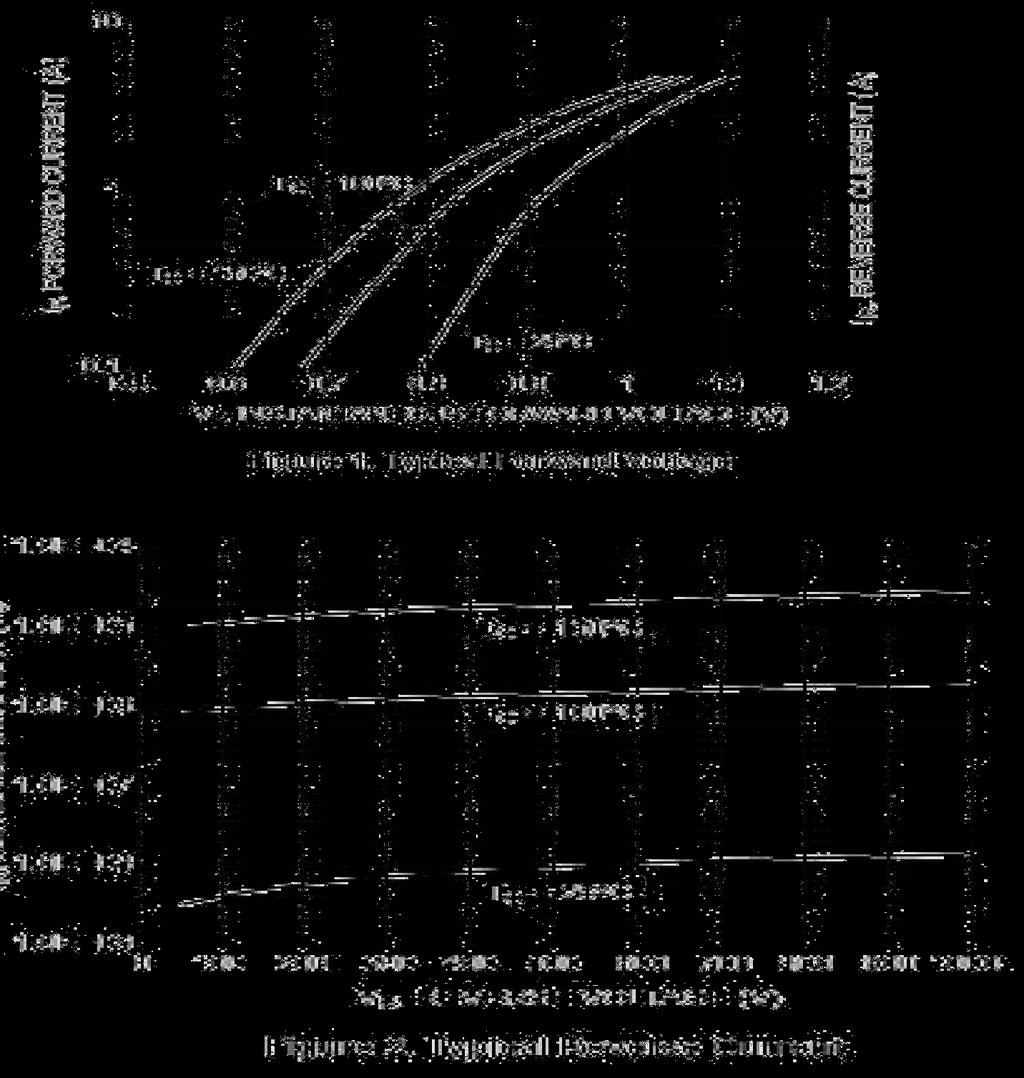
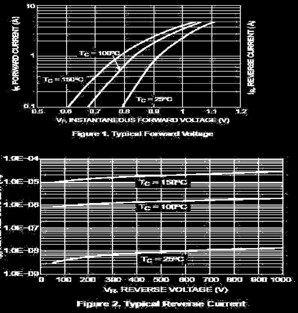
6 2. Curve tracers A curve tracer can display the characteristics of a host device. Device could be diode or transistor or other semiconductor device. Curve tracer by tektronix and other companies available Easy to use and testing with less effort and time. Diode specifications Data sheets provide data on specific semiconductor device. Manufacturers provide these information Usually given in easy readable formats like graphs, artwork, tables and so on., These specifications are required for proper utilization of devices for specific applications Important data to be considered are The forward voltage V F (at specific T) Maximum forward current I F Maximum reverse saturation current I R The reverse voltage rating (PIV) Maximum power dissipation Capacitance levels Reverse recovery time t rr Operating temperature range Depending on type of diode being used, additional data such as Frequency Noise level Switching time Thermal resistance Peak repetitive values are also provided
7 For IN4001 and 4007 Maximum ratings are those values beyond which device damage can occur.
8


9 Zener diodes By proper doping of the silicon, the Zener Breakdown can be made to have a very sharp breakdown. The breakdown voltage is commonly labeled as VZ. Characteristics of Zener diode Equivalent circuit consist of a constant voltage supply of V Z in series with a zener resistor r Z.
10 The approximate model is obtained just by neglecting the effect of r Z in the equivalent model. Only a constant voltage source is used in this model. The temperature coefficients reflects the percentage change in V Z with temperature and it is defined by the relation T c ={ V Z / V Z ( T 1 -T 0 ) } x 100% V Z change in zener potential due to temperature variation (T 1 -T 0 ) change in temperature Examples 1. Det. Nominal voltage for 1N961 fairchild zener diode at temp of c. Solution: V Z =T c V Z (T 1 -T 0 )/100 ={0.072x10V/100}( ) = 0.54V Therefore change in Zener voltage is 10.54V when temperature is raised from 25 0 c to c. 2. Find Is and vl using zener characteristics for given data. 3. Compute the Thevenin equivalent of the previous circuit with the zener diode as the load Thevenin voltage Thevenin resistance We can then write VT +RTiD+vD = 0 and find out vd,, id using the zener diode characteristics
11 vl = vd and IS = vl /RL + id Solution Answers vl = 10V IS = vl /RL + id = 10/6 +10 ma = 11.67mA vl = 9.5 V IS = vl /RL + id = 9.5/ ma = 12.92mA
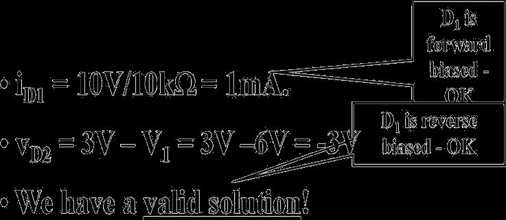
12 4. Find currents through diode D1 and D2. General Approach: Assume the state of each of the diodes: i.e., on or off. Analyze the circuit and check to see if your assumptions were correct. If not correct try another set of assumptions. Assume D1 is off : Replace with open Assume D2 is on : Replace with short vd1 = 10V 3V = 7V But this is not possible since the D1 would be forward biased or on with vd1 = 0V. We must try another set of assumptions Assume D1 is on and D2 is off
13 Example 2
Chapter 1: Semiconductor Diodes
 Chapter 1: Semiconductor Diodes Diodes The diode is a 2-terminal device. A diode ideally conducts in only one direction. 2 Diode Characteristics Conduction Region Non-Conduction Region The voltage across
Analog Electronics Circuits. Chapter 1: Diode circuits
 Analog Electronics Circuits Objective Chapter 1: Diode circuits To understand the diode operation and its equivalent circuits To understand various parameters of diodes Load line analysis Diode applications
Mechatronics Chapter 3-1 Semiconductor devices Diode
 MEMS1082 Mechatronics Chapter 3-1 Semiconductor devices Diode Semiconductor: Si Semiconductor N-type and P-type Semiconductors There are two types of impurities: N-type - In N-type doping, phosphorus or
The George Washington University School of Engineering and Applied Science Department of Electrical and Computer Engineering ECE 20 - LAB
 The George Washington University School of Engineering and Applied Science Department of Electrical and Computer Engineering ECE 20 - LAB Components: Experiment # 1 Solid State Diodes Testing & Characterization
Table of Contents. iii
 Table of Contents Subject Page Experiment 1: Diode Characteristics... 1 Experiment 2: Rectifier Circuits... 7 Experiment 3: Clipping and Clamping Circuits 17 Experiment 4: The Zener Diode 25 Experiment
Electro - Principles I
 The PN Junction Diode Introduction to the PN Junction Diode Note: In this chapter we consider conventional current flow. Page 11-1 The schematic symbol for the pn junction diode the shown in Figure 1.
Electronic Circuits I - Tutorial 03 Diode Applications I
 Electronic Circuits I - Tutorial 03 Diode Applications I -1 / 13 - T & F # Question 1 A diode can conduct current in two directions with equal ease. F 2 When reverse-biased, a diode ideally appears as
Shankersinh Vaghela Bapu Institute of Technology INDEX
 Shankersinh Vaghela Bapu Institute of Technology Diploma EE Semester III 3330905: ELECTRONIC COMPONENTS AND CIRCUITS INDEX Sr. No. Title Page Date Sign Grade 1 Obtain I-V characteristic of Diode. 2 To
LABORATORY 8 DIODE CIRCUITS
 LABORATORY 8 DIODE CIRCUITS A solid state diode consists of a junction of either dissimilar semiconductors (pn junction diode) or a metal and a semiconductor (Schottky barrier diode). Regardless of the
EXPERIMENT 7: DIODE CHARACTERISTICS AND CIRCUITS 10/24/10
 DIODE CHARACTERISTICS AND CIRCUITS EXPERIMENT 7: DIODE CHARACTERISTICS AND CIRCUITS 10/24/10 In this experiment we will measure the I vs V characteristics of Si, Ge, and Zener p-n junction diodes, and
Objective: To study and verify the functionality of a) PN junction diode in forward bias. Sl.No. Name Quantity Name Quantity 1 Diode
 PN junction diode in forward bias. Sl.No. Name Quantity Name Quantity 1 Diode") Experiment No: 1 Diode Characteristics Objective: To study and verify the functionality of a) PN junction diode in forward bias Components/ Equipments Required: b) Point-Contact diode in reverse bias Components
Experiment No: 1 Diode Characteristics Objective: To study and verify the functionality of a) PN junction diode in forward bias Components/ Equipments Required: b) Point-Contact diode in reverse bias Components
Experiment #1: Solid State Diodes Testing & Characterization. Type Value Symbol Name Multisim Part Description Resistor 1MΩ R 2 Basic/Resistor ---
 SCHOOL OF ENGINEERING AND APPLIED SCIENCE DEPARTMENT OF ELECTRICAL AND COMPUTER ENGINEERING ECE 2115: ENGINEERING ELECTRONICS LABORATORY Experiment #1: Solid State Diodes Testing & Characterization COMPONENTS
1) A silicon diode measures a low value of resistance with the meter leads in both positions. The trouble, if any, is
 A silicon diode measures a low value of resistance with the meter leads in both positions. The trouble, if any, is") 1) A silicon diode measures a low value of resistance with the meter leads in both positions. The trouble, if any, is A [ ]) the diode is open. B [ ]) the diode is shorted to ground. C [v]) the diode is
1) A silicon diode measures a low value of resistance with the meter leads in both positions. The trouble, if any, is A [ ]) the diode is open. B [ ]) the diode is shorted to ground. C [v]) the diode is
Page 1. Date 15/02/2013
 Page 1 Date 15/02/2013 Final Term Examination Fall 2012 Phy301-Circuit Theory 1. State kirchhoff s current law (KCL) Marks: 2: Answer: (PAGE 42) KIRCHHOF S CURRENT LAW Sum of all the currents entering
VTU NOTES QUESTION PAPERS NEWS RESULTS FORUMS TESTING OF DIODE CLIPPING CIRCUITS
 TESTING OF DIODE CLIPPING CIRCUITS Aim: Testing of diode clipping circuits. Apparatus required: Diode (1N4007/BY127), Resistor, DC regulated power supply, signal generator and CRO. Theory: The circuit
EXPERIMENT 3 Half-Wave and Full-Wave Rectification
 Name & Surname: ID: Date: EXPERIMENT 3 Half-Wave and Full-Wave Rectification Objective To calculate, compare, draw, and measure the DC output voltages of half-wave and full-wave rectifier circuits. Tools
RECTIFIERS AND POWER SUPPLIES
 UNIT V RECTIFIERS AND POWER SUPPLIES Half-wave, full-wave and bridge rectifiers with resistive load. Analysis for Vdc and ripple voltage with C,CL, L-C and C-L-C filters. Voltage multipliers Zenerdiode
Analog Electronic Circuits
 Analog Electronic Circuits Chapter 1: Semiconductor Diodes Objectives: To become familiar with the working principles of semiconductor diode To become familiar with the design and analysis of diode circuits
Term Roadmap : Materials Types 1. INSULATORS
 Term Roadmap : Introduction to Signal Processing Differentiating and Integrating Circuits (OpAmps) Clipping and Clamping Circuits(Diodes) Design of analog filters Sinusoidal Oscillators Multivibrators
ENG2210 Electronic Circuits. Chapter 3 Diodes
 ENG2210 Electronic Circuits Mokhtar A. Aboelaze York University Chapter 3 Diodes Objectives Learn the characteristics of ideal diode and how to analyze and design circuits containing multiple diodes Learn
EQUIVALENT EQUIPMENT CIRCUITS
 INTRODUCTION EQUIVALENT EQUIPMENT CIRCUITS The student will analyze the internal properties of the equipment used in lab. The input resistance of the oscilloscope and digital multimeter when used as a
A device which removes the peak of a waveform is known as a Clipper. Voltage clipping diagram
 DIODE CLIPPER A device which removes the peak of a waveform is known as a Clipper Voltage clipping diagram Clipping circuit Clipping circuit is a wave-shaping circuit, and is used to either remove or clip
Unit/Standard Number. LEA Task # Alignment
 1 Secondary Competency Task List 100 SAFETY 101 Demonstrate an understanding of State and School safety regulations. 102 Practice safety techniques for electronics work. 103 Demonstrate an understanding
Figure 1 Diode schematic symbol (left) and physical representation (right)
 and physical representation (right)") Page 1/7 Revision 1 20-Jul-10 OBJECTIVES To reinforce the concepts behind diode circuit analysis Verification of diode theory and operation To understand certain diode applications, such as rectification
Page 1/7 Revision 1 20-Jul-10 OBJECTIVES To reinforce the concepts behind diode circuit analysis Verification of diode theory and operation To understand certain diode applications, such as rectification
Lecture (03) Diodes and Diode Applications I
 Diodes and Diode Applications I") Lecture (03) Diodes and Diode Applications I By: Dr. Ahmed ElShafee ١ Agenda VOLTAGE CURRENT CHARACTERISTIC OF A DIODE Forward bias Reverse Bias V I Characteristic for Forward Bias V I Characteristic for
Lecture (03) Diodes and Diode Applications I By: Dr. Ahmed ElShafee ١ Agenda VOLTAGE CURRENT CHARACTERISTIC OF A DIODE Forward bias Reverse Bias V I Characteristic for Forward Bias V I Characteristic for
2) The larger the ripple voltage, the better the filter. 2) 3) Clamping circuits use capacitors and diodes to add a dc level to a waveform.
 The larger the ripple voltage, the better the filter. 2) 3) Clamping circuits use capacitors and diodes to add a dc level to a waveform.") TRUE/FALSE. Write 'T' if the statement is true and 'F' if the statement is false. 1) A diode conducts current when forward-biased and blocks current when reverse-biased. 1) 2) The larger the ripple voltage,
TRUE/FALSE. Write 'T' if the statement is true and 'F' if the statement is false. 1) A diode conducts current when forward-biased and blocks current when reverse-biased. 1) 2) The larger the ripple voltage,
Zener Diodes. Specifying and modeling the zener diode. - Diodes operating in the breakdown region can be used in the design of voltage regulators.
 Zener Diodes - Diodes operating in the breakdown region can be used in the design of voltage regulators. Specifying and modeling the zener diode Dynamic resistance, r Z a few ohms to a few tens of ohms
The preferred Exercise is shown in Exercises 5B or 5C.
 ECE 231 Laboratory Exercise 5A The preferred Exercise is shown in Exercises 5B or 5C. Laboratory Group (Names) OBJECTIVES Validate the Schottky diode equation. Calculate the dc and dynamic (ac) resistance
Physics 281 EXPERIMENT 7 I-V Curves of Non linear Device
 Physics 281 EXPERIMENT 7 I-V Curves of Non linear Device Print this page to start your lab report (1 copy) Bring a diskette to save your data. OBJECT: To study the method of obtaining the characteristics
Chapter 2. Diodes & Applications
 Chapter 2 Diodes & Applications The Diode A diode is made from a small piece of semiconductor material, usually silicon, in which half is doped as a p region and half is doped as an n region with a pn
Diodes and Applications
 Diodes and Applications Diodes and Applications 2 1 Diode Operation 2 2 Voltage-Current (V-I) Characteristics 2 3 Diode Models 2 4 Half-Wave Rectifiers 2 5 Full-Wave Rectifiers 2 6 Power Supply Filters
Experiments in Analog Electronics
 Ministry of Higher Education and Scientific Research University of Technology Department of Electrical Engineering Analog Electronics Laboratory Experiments in Analog Electronics By Firas Mohammed Ali
Federal Urdu University of Arts, Science & Technology Islamabad Pakistan SECOND SEMESTER ELECTRONICS - I
 SECOND SEMESTER ELECTRONICS - I BASIC ELECTRICAL & ELECTRONICS LAB DEPARTMENT OF ELECTRICAL ENGINEERING Prepared By: Checked By: Approved By: Engr. Yousaf Hameed Engr. M.Nasim Khan Dr.Noman Jafri Lecturer
IENGINEERS- CONSULTANTS QUESTION BANK SERIES ELECTRONICS ENGINEERING 1 YEAR UPTU
 ELECTRONICS ENGINEERING Unit 1 Objectives Q.1 The breakdown mechanism in a lightly doped p-n junction under reverse biased condition is called. (A) avalanche breakdown. (B) zener breakdown. (C) breakdown
3. Diode, Rectifiers, and Power Supplies
 3. Diode, Rectifiers, and Power Supplies Semiconductor diodes are active devices which are extremely important for various electrical and electronic circuits. Diodes are active non-linear circuit elements
SUMMER 13 EXAMINATION Subject Code: Model Answer Page No: / N
 Important Instructions to examiners: 1) The answers should be examined by key words and not as word-to-word as given in the model answer scheme. 2) The model answer and the answer written by candidate
The Norwegian University of Science and Technology ENGLISH. EXAM IN TFY 4185 Measurement Technique/Måleteknikk. 1 Dec 2014 Time: 09:00-13:00
 Page 1 of 9 The Norwegian University of Science and Technology ENGLISH Department of Physics Contact person: Name: Patrick Espy Tel: +47 73 55 10 95 (office) or +47 41 38 65 78 (mobile) EXAM IN TFY 4185
Entry Level Assessment Blueprint Electronics
 Entry Level Assessment Blueprint Electronics Test Code: 3034 / Version: 01 Specific Competencies and Skills Tested in this Assessment: Safety Demonstrate understanding of SDS Exhibit understanding of ESD
Revised April Unit/Standard Number. Proficiency Level Achieved: (X) Indicates Competency Achieved to Industry Proficiency Level
 Indicates Competency Achieved to Industry Proficiency Level") Unit/Standard Number Electrical, Electronic and Communications Engineering Technology/Technician CIP 15.0303 Task Grid Secondary Competency Task List 100 SAFETY 101 Demonstrate an understanding of state,
Unit/Standard Number Electrical, Electronic and Communications Engineering Technology/Technician CIP 15.0303 Task Grid Secondary Competency Task List 100 SAFETY 101 Demonstrate an understanding of state,
Applications of diodes
 Applications of diodes Learners should be able to: (a) describe the I V characteristics of a silicon diode (b) describe the use of diodes for component protection in DC circuits and half-wave rectification
EC6202- ELECTRONIC DEVICES AND CIRCUITS UNIT TEST-1 EXPECTED QUESTIONS
 EC6202- ELECTRONIC DEVICES AND CIRCUITS UNIT TEST-1 EXPECTED QUESTIONS 1. List the PN diode parameters. 1. Bulk Resistance. 2. Static Resistance/Junction Resistance (or) DC Forward Resistance 3. Dynamic
EECE 2413 Electronics Laboratory
 EECE 2413 Electronics Laboratory Lab #2: Diode Circuits Goals In this lab you will become familiar with several different types of pn-junction diodes. These include silicon and germanium junction diodes,
Revised April Unit/Standard Number. High School Graduation Years 2016, 2017 and 2018
 Unit/Standard Number High School Graduation Years 2016, 2017 and 2018 Electrical, Electronic and Communications Engineering Technology/Technician CIP 15.0303 Task Grid Secondary Competency Task List 100
Exercise 12. Semiconductors EXERCISE OBJECTIVE DISCUSSION OUTLINE DISCUSSION. Introduction to semiconductors. The diode
 Exercise 12 Semiconductors EXERCISE OBJECTIVE When you have completed this exercise, you will be familiar with the operation of a diode. You will learn how to use a diode to rectify ac voltage to produce
Electron Devices and Circuits (EC 8353)
") Electron Devices and Circuits (EC 8353) Prepared by Ms.S.KARKUZHALI, A.P/EEE Diodes The diode is a 2-terminal device. A diode ideally conducts in only one direction. Diode Characteristics Conduction Region
Electron Devices and Circuits (EC 8353) Prepared by Ms.S.KARKUZHALI, A.P/EEE Diodes The diode is a 2-terminal device. A diode ideally conducts in only one direction. Diode Characteristics Conduction Region
Department of Electrical and Electronics Engineering Logic Circuits Laboratory EXPERIMENT-1 BASIC GATE CIRCUITS
 1.1 Preliminary Study Simulate experiment using an available tool and prepare the preliminary report. 1.2 Aim of the Experiment Implementation and examination of logic gate circuits and their basic operations.
Lecture 6: Zener Diodes.
 Whites, EE 320 Lecture 6 Page 1 of 11 Lecture 6: Zener Diodes. The very steep portion in the reverse biased i-v characteristic curve is called the breakdown region. In this region the voltage across the
SKEU 3741 BASIC ELECTRONICS LAB
 Faculty: Subject Subject Code : SKEU 3741 FACULTY OF ELECTRICAL ENGINEERING : 2 ND YEAR ELECTRONIC DESIGN LABORATORY Review Release Date Last Amendment Procedure Number : 1 : 2013 : 2013 : PK-UTM-FKE-(0)-10
Lecture -1: p-n Junction Diode
 Lecture -1: p-n Junction Diode Diode: A pure silicon crystal or germanium crystal is known as an intrinsic semiconductor. There are not enough free electrons and holes in an intrinsic semi-conductor to
Equivalent Equipment Circuits
 1. Introduction Equivalent Equipment Circuits The student will analyze the internal properties of the equipment used in lab. The input resistance of the oscilloscope and Digital MultiMeter (DMM) when used
EXPERIMENTS USING SEMICONDUCTOR DIODES
 EXPERIMENT 9 EXPERIMENTS USING SEMICONDUCTOR DIODES Semiconductor Diodes Structure 91 Introduction Objectives 92 Basics of Semiconductors Revisited 93 A p-n Junction Operation of a p-n Junction A Forward
CHAPTER 1 DIODE CIRCUITS. Semiconductor act differently to DC and AC currents
 CHAPTER 1 DIODE CIRCUITS Resistance levels Semiconductor act differently to DC and AC currents There are three types of resistances 1. DC or static resistance The application of DC voltage to a circuit
Objective Type Questions 1. Why pure semiconductors are insulators at 0 o K? 2. What is effect of temperature on barrier voltage? 3.
 Objective Type Questions 1. Why pure semiconductors are insulators at 0 o K? 2. What is effect of temperature on barrier voltage? 3. What is difference between electron and hole? 4. Why electrons have
semiconductor p-n junction Potential difference across the depletion region is called the built-in potential barrier, or built-in voltage:
 Chapter four The Equilibrium pn Junction The Electric field will create a force that will stop the diffusion of carriers reaches thermal equilibrium condition Potential difference across the depletion
Mechatronics and Measurement. Lecturer:Dung-An Wang Lecture 2
 Mechatronics and Measurement Lecturer:Dung-An Wang Lecture 2 Lecture outline Reading:Ch3 of text Today s lecture Semiconductor 2 Diode 3 4 Zener diode Voltage-regulator diodes. This family of diodes exhibits
Experiment 2 Electric Circuit Fundamentals
 Experiment 2 Electric Circuit Fundamentals Introduction This experiment has two parts. Each part will have to be carried out using the Multisim Electronics Workbench software. The experiment will then
EXPERIMENT 5 CURRENT AND VOLTAGE CHARACTERISTICS OF BJT
 EXPERIMENT 5 CURRENT AND VOLTAGE CHARACTERISTICS OF BJT 1. OBJECTIVES 1.1 To practice how to test NPN and PNP transistors using multimeter. 1.2 To demonstrate the relationship between collector current
Summer 2015 Examination. 1) The answers should be examined by key words and not as word-to-word as given in the model answer scheme.
 The answers should be examined by key words and not as word-to-word as given in the model answer scheme.") Summer 2015 Examination Subject Code: 17215 Model Answer Important Instructions to examiners: 1) The answers should be examined by key words and not as word-to-word as given in the model answer scheme.
Summer 2015 Examination Subject Code: 17215 Model Answer Important Instructions to examiners: 1) The answers should be examined by key words and not as word-to-word as given in the model answer scheme.
INSTITUTE OF AERONAUTICAL ENGINEERING (Autonomous) Dundigal, Hyderabad
 Dundigal, Hyderabad") I INSTITUTE OF AERONAUTICAL ENGINEERING (Autonomous) Dundigal, Hyderabad-500043 CIVIL ENGINEERING TUTORIAL QUESTION BANK Course Name : BASIC ELECTRICAL AND ELECTRONICS ENGINEERING Course Code : AEE018
I INSTITUTE OF AERONAUTICAL ENGINEERING (Autonomous) Dundigal, Hyderabad-500043 CIVIL ENGINEERING TUTORIAL QUESTION BANK Course Name : BASIC ELECTRICAL AND ELECTRONICS ENGINEERING Course Code : AEE018
NEW HORIZON PRE UNIVERSITY COLLEGE LESSON PLAN FOR THE ACADEMIC YEAR Department of ELECTRONICS
 NEW HORIZON PRE UNIVERSITY COLLEGE LESSON PLAN FOR THE ACADEMIC YEAR 2017 2018 Department of ELECTRONICS I PUC Month: JUNE I 1. INTRODUCTION TO ELECTRONICS Electronics and its scope: Development of vacuum
1. An engineer measures the (step response) rise time of an amplifier as. Estimate the 3-dB bandwidth of the amplifier. (2 points)
 rise time of an amplifier as. Estimate the 3-dB bandwidth of the amplifier. (2 points)") Exam 1 Name: Score /60 Question 1 Short Takes 1 point each unless noted otherwise. 1. An engineer measures the (step response) rise time of an amplifier as. Estimate the 3-dB bandwidth of the amplifier.
Exam 1 Name: Score /60 Question 1 Short Takes 1 point each unless noted otherwise. 1. An engineer measures the (step response) rise time of an amplifier as. Estimate the 3-dB bandwidth of the amplifier.
EE/COE 152: Basic Electronics. Lecture 3. A.S Agbemenu. https://sites.google.com/site/agbemenu/courses/ee-coe-152
 EE/COE 152: Basic Electronics Lecture 3 A.S Agbemenu https://sites.google.com/site/agbemenu/courses/ee-coe-152 Books: Microelcetronic Circuit Design (Jaeger/Blalock) Microelectronic Circuits (Sedra/Smith)
Pre-certification Electronics Questions. Answer the following with the MOST CORRECT answer.
 Electronics Questions Answer the following with the MOST CORRECT answer. 1. The cathode end terminal of a semiconductor diode can be identified by: a. the negative sign marked on the case b. a circular
PN Junction Diode Table of Contents. What Are Diodes Made Out Of?
 PN Junction iode Table of Contents What are diodes made out of?slide 3 N-type materialslide 4 P-type materialslide 5 The pn junctionslides 6-7 The biased pn junctionslides 8-9 Properties of diodesslides
EDC Lecture Notes UNIT-1
 P-N Junction Diode EDC Lecture Notes Diode: A pure silicon crystal or germanium crystal is known as an intrinsic semiconductor. There are not enough free electrons and holes in an intrinsic semi-conductor
MEASUREMENTS & INSTRUMENTATION ANALOG AND DIGITAL METERS
 MEASUREMENTS & INSTRUMENTATION ANALOG AND DIGITAL METERS ANALOG Metering devices Provides monotonous (continuous) movement. ELECTRICAL MEASURING INSTRUMENTS ANALOG METERS A d Arsonval galvanometer (Moving
Field - Effect Transistor
 Page 1 of 6 Field - Effect Transistor Aim :- To draw and study the out put and transfer characteristics of the given FET and to determine its parameters. Apparatus :- FET, two variable power supplies,
Class XII - Physics Semiconductor Electronics. Chapter-wise Problems
 lass X - Physics Semiconductor Electronics Materials, Device and Simple ircuit hapter-wise Problems Multiple hoice Question :- 14.1 The conductivity of a semiconductor increases with increase in temperature
CHADALAWADA RAMANAMMA ENGINEERING COLLEGE (AUTONOMOUS) Chadalawada Nagar, Renigunta Road, Tirupati
 Chadalawada Nagar, Renigunta Road, Tirupati") ELECTRONIC DEVICES AND CIRCUITS LABORATORY MANUAL Subject Code : 17CA04305 Regulations : R17 Class : III Semester (ECE) CHADALAWADA RAMANAMMA ENGINEERING COLLEGE (AUTONOMOUS) Chadalawada Nagar, Renigunta
ELECTRONIC DEVICES AND CIRCUITS LABORATORY MANUAL Subject Code : 17CA04305 Regulations : R17 Class : III Semester (ECE) CHADALAWADA RAMANAMMA ENGINEERING COLLEGE (AUTONOMOUS) Chadalawada Nagar, Renigunta
GUJARAT TECHNOLOGICAL UNIVERSITY BE - SEMESTER III EXAMINATION SUMMER 2013
 Seat No.: Enrolment No. GUJARAT TECHNOLOGICAL UNIVERSITY BE - SEMESTER III EXAMINATION SUMMER 2013 Subject Code: 131101 Date: 31-05-2013 Subject Name: Basic Electronics Time: 02.30 pm - 05.00 pm Total
KOM2751 Analog Electronics :: Dr. Muharrem Mercimek :: YTU - Control and Automation Dept. 1 1 (CONT D) DIODES
 DIODES") KOM2751 Analog Electronics :: Dr. Muharrem Mercimek :: YTU - Control and Automation Dept. 1 1 (CONT D) DIODES Most of the content is from the textbook: Electronic devices and circuit theory, Robert L.
KOM2751 Analog Electronics :: Dr. Muharrem Mercimek :: YTU - Control and Automation Dept. 1 1 (CONT D) DIODES Most of the content is from the textbook: Electronic devices and circuit theory, Robert L.
Diode Characteristics and Applications
 Diode Characteristics and Applications Topics covered in this presentation: Diode Characteristics Diode Clamp Protecting Against Back-EMF Half-Wave Rectifier The Zener Diode 1 of 18 Diode Characteristics
EC T34 ELECTRONIC DEVICES AND CIRCUITS
 RAJIV GANDHI COLLEGE OF ENGINEERING AND TECHNOLOGY PONDY-CUDDALORE MAIN ROAD, KIRUMAMPAKKAM-PUDUCHERRY DEPARTMENT OF ECE EC T34 ELECTRONIC DEVICES AND CIRCUITS II YEAR Mr.L.ARUNJEEVA., AP/ECE 1 PN JUNCTION
UNIT 4 BIASING AND STABILIZATION
 UNIT 4 BIASING AND STABILIZATION TRANSISTOR BIASING: To operate the transistor in the desired region, we have to apply external dec voltages of correct polarity and magnitude to the two junctions of the
Chapter 1: Diode circuits
 Analog Electronics Circuits Nagamani A N Lecturer, PESIT, Bangalore 85 Email nagamani@pes.edu Chapter 1: Diode circuits Objective To understand the diode operation and its equivalent circuits To understand
Diode Limiters or Clipper Circuits
 Diode Limiters or Clipper Circuits Circuits which are used to clip off portions of signal voltages above or below certain levels are called limiters or clippers. Types of Clippers Positive Clipper Negative
Electronics Laboratory And Students kits For Self-Study And Distant Learning. By: Charbel T. Fahed
 Electronics Laboratory And Students kits For Self-Study And Distant Learning By: Charbel T. Fahed Table of Contents I. DC and AC fundamentals 1) Color Code 2) Ohm s Law 3) Series Circuits 4) Parallel Circuits
UNIT IX ELECTRONIC DEVICES
 UNT X ELECTRONC DECES Weightage Marks : 07 Semiconductors Semiconductors diode-- characteristics in forward and reverse bias, diode as rectifier. - characteristics of LED, Photodiodes, solarcell and Zener
55:041 Electronic Circuits
 55:041 Electronic Circuits Chapter 1 & 2 A. Kruger Diode Review, Page-1 Semiconductors licon () atoms have 4 electrons in valence band and form strong covalent bonds with surrounding atoms. Section 1.1.2
R. W. Erickson. Department of Electrical, Computer, and Energy Engineering University of Colorado, Boulder
 R. W. Erickson Department of Electrical, Computer, and Energy Engineering University of Colorado, Boulder Inclusion of Switching Loss in the Averaged Equivalent Circuit Model The methods of Chapter 3 can
UNIVERSITY OF TECHNOLOGY, JAMAICA SCHOOL OF ENGENEERING. Electrical Engineering Science. Laboratory Manual
 UNIVERSITY OF TECHNOLOGY, JAMAICA SCHOOL OF ENGENEERING Electrical Engineering Science Laboratory Manual Table of Contents Experiment #1 OHM S LAW... 3 Experiment # 2 SERIES AND PARALLEL CIRCUITS... 8
Shankersinh Vaghela Bapu Institute of Technology
 Shankersinh Vaghela Bapu Institute of Technology B.E. Semester III (EC) 131101: Basic Electronics INDEX Sr. No. Title Page Date Sign Grade 1 [A] To Study the V-I characteristic of PN junction diode. [B]
SCRIPT. Voltage Dividers
 SCRIPT Hello friends in our earlier discussion we talked about series resistive circuits, when connected in series, resistors form a "string" in which there is only one path for current. Ohm's law can
Perkins Statewide Articulation Agreement. Documentation item: Secondary Competency Task List Coversheet
 Perkins Statewide Articulation Agreement Documentation item: Secondary Task List Coversheet The Secondary School agrees to: A. Implement the approved PDE Program(s) of Study. B. Provide assessment of student
DC Bias. Graphical Analysis. Script
 Course: B.Sc. Applied Physical Science (Computer Science) Year & Sem.: Ist Year, Sem - IInd Subject: Electronics Paper No.: V Paper Title: Analog Circuits Lecture No.: 3 Lecture Title: Analog Circuits
DE52/DC52 FUNDAMENTALS OF ELECTRICAL & ELECT ENGG DEC 2014
 Q.2 a. Derive an expression for the current flowing at any instant during the discharge of a capacitor C across a resistor R. b. The coil of a moving coil instrument is wound with 50 turns of wire. The
PHYS 1402 General Physics II Experiment 5: Ohm s Law
 PHYS 1402 General Physics II Experiment 5: Ohm s Law Student Name Objective: To investigate the relationship between current and resistance for ordinary conductors known as ohmic conductors. Theory: For
UNIT 3: FIELD EFFECT TRANSISTORS
 FIELD EFFECT TRANSISTOR: UNIT 3: FIELD EFFECT TRANSISTORS The field effect transistor is a semiconductor device, which depends for its operation on the control of current by an electric field. There are
Ohm s Law and Electrical Circuits
 Ohm s Law and Electrical Circuits INTRODUCTION In this experiment, you will measure the current-voltage characteristics of a resistor and check to see if the resistor satisfies Ohm s law. In the process
EXPERIMENT 5 : DIODES AND RECTIFICATION
 EXPERIMENT 5 : DIODES AND RECTIFICATION Component List Resistors, one of each o 2 1010W o 1 1k o 1 10k 4 1N4004 (Imax = 1A, PIV = 400V) Diodes Center tap transformer (35.6Vpp, 12.6 VRMS) 100 F Electrolytic
FINALTERM EXAMINATION. Spring PHY301- Circuit Theory
 Date 14/2/2013 Eini FINALTERM EXAMINATION Spring 2010 PHY301- Circuit Theory Time: 90 min Marks: 60 Question No: 1 If we connect 3 capacitors in parallel, the combined effect of all these capacitors will
A.C voltmeters using rectifier
 Lecture 5 A.C voltmeters using rectifier The PMMC movement used in d.c. voltmeters can be effectively used in a.c. voltmeters. The rectifier is used to convert a.c. voltage to be measured, to d.c. This
Intrinsic Semiconductor
 Semiconductors Crystalline solid materials whose resistivities are values between those of conductors and insulators. Good electrical characteristics and feasible fabrication technology are some reasons
Module 1, Lesson 2 Introduction to electricity. Student. 45 minutes
 Module 1, Lesson 2 Introduction to electricity 45 minutes Student Purpose of this lesson Explanations of fundamental quantities of electrical circuits, including voltage, current and resistance. Use a
Basic Electronic Devices and Circuits EE 111 Electrical Engineering Majmaah University 2 nd Semester 1432/1433 H. Chapter 2. Diodes and Applications
 Basic Electronic Devices and Circuits EE 111 Electrical Engineering Majmaah University 2 nd Semester 1432/1433 H Chapter 2 Diodes and Applications 1 Diodes A diode is a semiconductor device with a single
55:041 Electronic Circuits
 55:041 Electronic Circuits Chapter 1 & 2 A. Kruger Diode Review, Page-1 Semiconductors licon () atoms have 4 electrons in valence band and form strong covalent bonds with surrounding atoms. Section 1.1.2
Charge Current Voltage
 ECE110 Introduction to Electronics What is? Charge Current Voltage 1 Kirchhoff s Current Law Current in = Current out Conservation of charge! (What goes in must come out, or the total coming in is zero)
Fig [5]
![Fig [5]](/thumbs/82/85456687.jpg "Fig [5]") 1 (a) Fig. 4.1 shows the I-V characteristic of a light-emitting diode (LED). 40 I / 10 3 A 30 20 10 0 1.0 1.5 2.0 V / V Fig. 4.1 (i) In Describe the significant features of the graph in terms of current,
1 (a) Fig. 4.1 shows the I-V characteristic of a light-emitting diode (LED). 40 I / 10 3 A 30 20 10 0 1.0 1.5 2.0 V / V Fig. 4.1 (i) In Describe the significant features of the graph in terms of current,
 ANNA UNIVERSITY, Chennai 2013 REGULATION DEPARTMENT OF ELECTRONICS & COMMUNICATION ENGG. EC6211 CIRCUITS AND DEVICES LABORATORY (I B.E II Semester Batch 2013) EC6211 CIRCUITS AND DEVICES LABORATORY List
UNIVERSITY OF TECHNOLOGY, JAMAICA School of Engineering -
 UNIVERSITY OF TECHNOLOGY, JAMAICA School of Engineering - Electrical Engineering Science Laboratory Manual Table of Contents Safety Rules and Operating Procedures... 3 Troubleshooting Hints... 4 Experiment