MPI Halbleiterlabor. Detectors for the experiments at FLASH, LCLS, SCSS and XFEL. CFEL inside. MPI Semiconductor Laboratory
|
|
|
- Aubrie Marianna Hoover
- 6 years ago
- Views:
Transcription


1 CFEL inside MPI Halbleiterlabor MPI Semiconductor Laboratory Detectors for the experiments at FLASH, LCLS, SCSS and XFEL The fine art of high speed X-ray imaging UNIVERSITÄT SIEGEN


2 MPI für extraterrestische Physik (MPE) The MPI Semiconductor Laboratory High speed, low noise, low power, radiation hard, high Q.E.... Home made imaging X-ray detectors systems Feb 7, 2007 E. Lama, N. Kimmel, O. Hälker, S. Herrmann, T. Lauf, E. Hyde, N. Meidinger, D. Miessner, G. Hasinger, F. Schopper, G. Schaller, M. Porro, J. Treis, S. Wölfel, C. Zhang, P. Holl, P. Lechner, R. Eckardt, I. Radivojevic, R. Andritschke, L. Strüder A. Bechtel, O. Jaritschin, R. MPI für extraterrestrische Physik M. Schnecke, R. Richter, Hartmann, K. Heinzinger, C. Koitsch, A. Wassatsch H. Soltau, G. Lutz, C. Reich, G. Signeri, F. Hempelmann, Max-Planck-Institut für Physik
 Lothar Strüder, Rainer Richter, Matteo Porro, Florian Schopper, Gabi Schächner, Danilo Miessner, Martina Schnecke, Thomas Lauf, Gerhard Schaller, Norbert Meidinger, Sven")
3 Prepared by 1. MPI-HLL (MPE and MPP) Lothar Strüder, Rainer Richter, Matteo Porro, Florian Schopper, Gabi Schächner, Danilo Miessner, Martina Schnecke, Thomas Lauf, Gerhard Schaller, Norbert Meidinger, Sven Herrmann, Laci Andricek, Gerhard Fuchs, Johannes Treis, Nils Kimmel, Robert Andritschke, Zdenka Albrechtskirchinger, Valentin Fedl, Giulio de Vita, Georg Weidenspointner, A. Wassatsch, Hans-Günther Moser, Admir Ramic, Gerhard Fuchs Daniel Pietschner, Johannes Elbs, Olaf Hälker, Toboas Panzner, Stefanie Ebermayer, Sebastian Hasinger, Florian Aschauer, Alexander Bähr, 2. PNSensor and PNDetector Heike Soltau, Robert Hartmann, Peter Lechner, Peter Holl, Rouven Eckhart, Adrian Nicolae, Klaus Heinzinger, Christian Koitsch, Andreas Liebel, Alois Bechteler, Uwe Weichert, Olga Jaritschin, Gerhard Lutz, Sebastian Ihle, Gabriele Signeri, Ivan Ordavo Christian Reich, Christian Thamm, Kathrin Hermenau, Markus Kufner Adrian Niculae, Armin Schön, Barbara Titze, Samantha Jeschke Melanie Schulze
4 OUTLINE Fully depleted, high speed, monolithic, large format pnccds and DePFETs are being or will be - used from 50 ev to 25 kev for spectroscopic and intensity imaging at the FLASH, Petra III, LCLS and XFEL synchrotrons: SDDs pnccds LSDDs DEPFET APS gatable DEPFETs RNDR
5 OUTLINE Fully depleted, high speed, monolithic, large format pnccds and DePFETs are being or will be - used from 50 ev to 25 kev for spectroscopic and intensity imaging at the FLASH, Petra III, LCLS and XFEL synchrotrons: SDDs pnccds LSDDs first part DEPFET APS gatable DEPFETs RNDR

6 OUTLINE Fully depleted, high speed, monolithic, large format pnccds and DePFETs are being or will be - used from 50 ev to 25 kev for spectroscopic and intensity imaging at the FLASH, Petra III, LCLS and XFEL synchrotrons: SDDs pnccds LSDDs DEPFET APS gatable DEPFETs RNDR second part
7 Requirements of the FLASH, LCLS and XFEL FLASH, LCLS + XFEL pnccd and DePFET system single photon resolution yes yes energy range 0.05 < E < 24 (kev) 0.05 < E < 25 [kev] pixel size (µm) (250) sig.rate/pixel/bunch 10 3 (10 5 ) quantum efficiency > 0.8 > 0.8 from 0.3 to 12 kev number of pixels 512 x 512 (min.) 1024 x 1024 and 2048 x 2048 frame rate/repetition rate 10 Hz Hz up to 250 Hz with pnccd XFEL burst mode 5 MHz (3.000 bunches) > 5 MHz (3.000 bunches) with DePFET system Readout noise < 150 e - (rms) < 30 e - (rms) (2 e - possible) cooling possible - 20 o C optimum room temperature possible
8 What is the challenge for XFEL Time structure: difference with others Electron bunch trains; up to 3000 bunches in 600 µsec, repeated 10 times per second. Producing 100 fsec X-ray pulses (up to bunches per second). 100 ms 100 ms 600 µs 99.4 ms 200 ns X-ray photons fs FEL process
9 What is the challenge for XFEL Time structure: difference with others Electron bunch trains; up to 3000 bunches in 600 µsec, repeated 10 times per second. Producing 100 fsec X-ray pulses (up to bunches per second). 600 µs 100 ms 100 ms 99.4 ms bunches/s but 99.4 ms (%) no photons 200 ns X-ray photons fs FEL process


10 What is limiting the quantum efficiency? The thickness of Silicon!! Q.E. = kev d = 2 mm Q.E. = kev d = 0.5 mm
11 Monolithic Integration of optical blocking filters Thin entrance window Silicon entrance window with x nm of SiO 2 and y nm of Si 3 N 4 plus z nm of Al (optical shield) optical light attenuation: ev 5 kev
12 I. the pnccd for operations up to 250 frames per sec

13 II. the DePFET active pixel sensor for 200 ns frame acquisition time


14 CCD basics full depletion (50 µm to 500 µm) back side illumination radiation hardness high readout speed pixel sizes from 36 µm to 650 µm charge handling: more than 106 e-/pixel high quantum efficiency SLAC, Menlo Park Lothar Strüder, MPI Halbleiterlabor and Universität Siegen


15 How many charges can be stored What determines the charge handling capacity in a pixel? pixel volume: 20x40x12 µm 3 1x10 4 µm 3 Doping: 10 2 P per µm 3 CHC = 1 x 10 6 per pixel can be increased by external voltages
16
17 Hard X-ray SASE Free Electron Lasers LINAC COHERENT LIGHT SOURCE LCLS 2009 European XFEL Facility SCSS SPring-8 Compact SASE Source
18 Hard X-ray SASE Free Electron Lasers LINAC COHERENT LIGHT SOURCE LCLS SCSS SPring-8 Compact SASE Source European XFEL Facility 2013 FLASH in operation
19 Hard X-ray SASE Free Electron Lasers LINAC COHERENT LIGHT SOURCE LCLS SCSS SPring-8 Compact SASE Source European XFEL Facility 2013 FLASH in operation FLASH: the ice breaker for XFELs


20 Hard X-ray SASE Free Electron Lasers LINAC COHERENT LIGHT SOURCE LCLS SCSS SPring-8 Compact SASE Source FLASH: 5 Hz, 10 Hz and 5 MHz LCLS: 120 Hz European XFEL Facility 2013 FLASH in operation FLASH: the ice breaker for XFELs SCSS: XFEL: 60 Hz 5 Hz, 10 Hz and 5 MHz
21 Detectors for FLASH+LCLS+XFEL 16 outputs device fabrication is finished now CMX CMX CMX CMX transfer of signal charges insensitive gaps: 800 µm Chip 1: area 29.5 cm 2 format: 1024 x 512 hole diameter: 3 mm Chip 2: area 29.5 cm 2 format: 1024 x 512 The full sensitive area of the system is 59 cm 2 with 75 µm pixels, 1024 x 1024 Full Frame imaging area per chip 512 x 1024 CMX CMX CMX CMX 16 outputs total area per chip: 29.5 cm 2 pixel size 75x75 µm 2 readout time per frame: 4 ms i.e. 250 fps can be triggered externally Total sensitive system area: 59 cm
22 pnccd: 1024 x 512, 30 cm pixel, 7.8 cm Area: 29.6 cm pixel, 3.7 cm Imaging 7.8 x 3.7 cm 2 = 29.6 cm 2 75 x 75 µm parallel read nodes 2 e 250 fps for 6 kev X-rays the system delivers 4k x 4k resolution points in all the area with less than one photon per pixel (typ. 90 %)

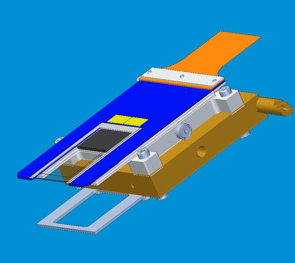
23 Flex lead ceramic carrier for thermal and structural support Flex lead CCD1 Flex lead CCD2 look at radiation entrance Flex lead for window side - power - control - signal out

24 pnccds overlapping in the center 800 µm insensitive gap Electrical components al components CCD1 Center hole CCD2 Electrical components Ceramic board Electrical components Mechanical thermal structure

25 The CFEL-ASG Chamber Reaction microscope: Many particle ion and electron imaging spectrometer Velocity map imaging Additional feautures: Integration of jet-targets,ports for lasers, special injectors support structures for fixed targets, etc...
 = 5 cm and P max with d(p IA ;P max ) = 300 mm.")
26 The CFEL-ASG Chamber Imaging system: For inside view the housing of C1 and C2 is drawn transparently. Detector 1 can have any position between P min with d(p IA ;P min ) = 5 cm and P max with d(p IA ;P max ) = 300 mm. Detector 2 is mounted fixed at d(p ;P ) = 500 mm.

27 The Imager of the CFEL-ASG Chamber Imaging system: (a) format 1024x1024, pixel size 75x75 µm 2, 8x8 cm 2 focal surface (b) center hole, typically 3 mm Due to overlap of the two detectors, effective insensitive area can be reduced to 1.6 mm, insensitive gaps: 0.8 mm (c) movement in y-direction: up to 45 mm


28 The Imager of the CFEL-ASG Chamber System alignment: Detector 1 is movable in Y, Z and X (limited), 400 mm Ø Detector 2 is fixed, 250 mm Ø
29 Detectors for FLASH+XFEL+PETRA III devices are scheduled for fabrication end 2009 ready: end 2010 The full sensitive area of the system is 239 cm 2 with 75 µm pixels, 2048 x 2048 CMX CMX CMX CMX Chip 1: area 59 cm 2 format: 1024 x 1024 transfer of charges Full Frame imaging, format per chip 1024 x 1024 total area per chip: 59 cm 2, per system: 236 cm 2 readout time per frame: 8 ms i.e. 125 fps pixel size 75x75 µm 2 This system is 3 side buttable, can be extended to a 2048 x 2048 array 16 outputs
30 FLASH, PETRA III and XFEL 2048 x 2048 CCD array (resolution points: 8kx8k) pixel size: 75 x 75 µm 2 total area: 236 cm 2 readout time: < 8 ms read noise < 15 electrons Charge handling capacity: > 1000 photons pp Energy 0.1<E<24 kev thickness: 500 µm


31 Recent pnccds fabrications flight type erosita version format: 384 x 384 x 2 pixel area: 8.4 cm cm 2 pixel size: 75 x 75 µm 2 prototype erosita version format: 256 x 256 x 2 pixel area: 3.7 cm cm 2 pixel size: 75 x 75 µm 2

32 Measurements with 512x256 FLASH + BESSY 256 parallel low noise readout channels with 2 or 4 output nodes Frame store area 256 x 256 pixel Imaging area 256 x 256 pixel
33 CAMEX block diagram Sr1 S1... S8 Sr1 G2 G4 G1 Vdd G3 IN Vbst Sin Stst BW1 BW2 BW3 Ss&h Smux OUT- OUT+ Vsss Tst current source JFET- amplifier passive lowpass filter CDS- filter sample & hold serializer cable driver digital control Vref master reference DAC(s) communication
 differential output buffer BIAS DACs BIAS master reference configuration")
34 CAMEX erosita 128I-JD 9153 um 128 x current source 6080 um 128 x AMP & CDS-filter S&H MUX CMX internal SEQ (shiftregister 16x64) differential output buffer BIAS DACs BIAS master reference configuration registers
 LVDS receivers generators of the")

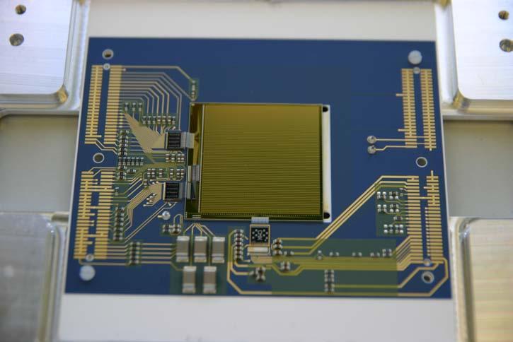
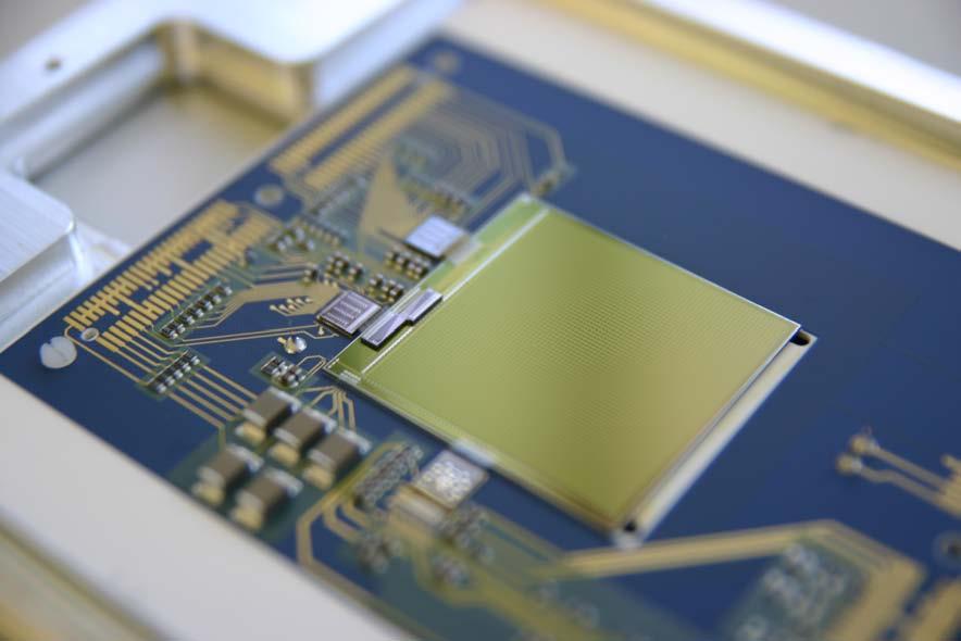
35 Development status: Flex lead + frontend PCB - connects CCD module to front-end PCB by wedge bonds - front-end PCB: analog output buffers (for the s, one per CAMEX) LVDS receivers generators of the analog CCD clock pulses (PHI drivers) connectors as electric interface to the camera electronics DUO flex lead: performance tested erosita flex lead: circuit diagram: under way layout: under way 29
36


37 Structure determination with a FEL Molecules atomic resolution Crystal J. Kirz, Nature Physics 2, 799 (2006) Lysozyme R. Neutze, J. Haidu et al., Nature 406, 752 (2000) Radiation damage and Coulomb explosion


38 Clusters in the Flight Xe clusters CFEL Detectors CCD camera nozzle skimmer cluster beam MCP detector + phosphor screen 550 nm visible light FEL beam aperture skimmer aperture VUV scattered light beam dump plane mirror

39 FLASH set-up in T.M. Beamline planar detector geometry in reflection mode CCD detector X-ray 90 ev Multilayer X-ray Mirror

40 First observation of 32 nm Xe nanocluster simulation of 90 ev X-rays scattering at single Xe nanoclusters with 32 nm size (C. Bostedt et al.) field of view of the pnccd during the experiment at the FLASH X-ray free electron laser facility at DESY, Hamburg
 FWHM: 38.9 ev s h ol d 30 ev T = -50 C Spectrum from 4.000 frames with 0.")
41 90 ev X-rays in single photon counting mode!!! t r i g g e r t h re E = 90 ev 25 ± 1.7 e-h pairs ENC = 2.5 e - (rms) FWHM: 38.9 ev s h ol d 30 ev T = -50 C Spectrum from frames with 0.05 photons/pixel/frame

42 Set-up in T.M. FLASH pnccd3 pnccd1 42 o 80 o 10 o 25 o pnccd2 20 o 40 o
43 Clusters in the Flight Collaboration: TU Berlin, MPI-HLL, MPI-K: Bostedt, Rupp, Adolph, Möller, Hartmann, Strüder, Rudenko, et al.
44 Free Electron Lasers Screen-Shots: To be evaluated!

45 Free Electron Lasers Screen-Shots: To be evaluated! SLAC, Menlo Park Lothar Strüder, MPI Halbleiterlabor and Universität Siegen

46 Clusters in the Flight Collaboration: TU Berlin, MPI-HLL, MPI-K: Bostedt, Rupp, Adolph, Möller, Hartmann, Strüder, Rudenko, et al.

47 Clusters in the Flight intensity / photons per pixel angle / deg
48 Clusters in the Flight intensity / photons per pixel angle / deg
49 Clusters in the Flight intensity / photons per pixel detector 1 detector 2 detector 3 angle / deg
50 Clusters in the Flight intensity / photons per pixel R = 83 nm detector 1 detector 2 detector 3 angle / deg
51 Clusters in the Flight intensity / photons per pixel R = 83 nm detector 1 detector 2 detector 3 R = 80 nm angle / deg
52 Clusters in the Flight intensity / photons per pixel Structure and Dynamics! detector 1 detector 2 detector 3 R = 83 nm R = 80 nm With strongly increased absorption! angle / deg
53 Bragg s law in energy space In angular space: λ=2 D sin α Peak distance : sinα n+1 sinα n 1/D Changing footprint area In energy space: E = hc/(2*d*sin α) E 6.2/(α*D) Peak distance : E n+1 E n 1/D


54 Useable spectral range Emission spectrum of BESSY II (1.7 GeV) Absorption by Air Usable energy range (measurement + calc.) Energy resolution of the detector < 150 ev 0.7 m air Useful spectrum kev

55 Langmuir-Blodgett-Film fixed angle of incidence Few minutes counting to photons per frame 400 to frames per second typical measurement times: 100 s to s position,time and energy resolved photons per spectrum: typ 10 8 α i = 0.8 deg
56 pnccd operating parameters Parameter Frame Store pnccd XMM type pnccd pixel size 36 µm, 48 µm, 51 µm and 75 µm 150 µm format x2, x2, x2, 512x x200, 400x400 active area (image only) 3.9 cm 2, 1.9 cm 2, 8.3 cm 2, 29 cm 2 3 cm 2, 36 cm 2 sensitive depth 450 µm 300 µm readout noise electrons (rms) 5 electrons (rms) Q.E. 90 % from 0.4 to 11 kev 90 % from 0.4 to 10 kev charge handling 5 x 10 5 electrons per pixel 5 x 10 5 e per pixel 6 kev 1 x x 10-5 E ev, kev --, kev readout time 10 µs or 20 µs per row 25 µs per row pixel rate 13 Mpix or 25 Mpix per second 2.8 Mpix per second frame rate up to 900 fps, 20 fps for erosita 14 fps out-of time events 0.2 % in the case of erosita 6%
. 100 ms 100 ms 600 µs 99.")
57 What is the challenge for XFEL Time structure: difference with others Electron bunch trains; up to 3000 bunches in 600 µsec, repeated 10 times per second. Producing 100 fsec X-ray pulses (up to bunches per second). 100 ms 100 ms 600 µs 99.4 ms 200 ns X-ray photons fs FEL process
58 Original LSDD Concept: reduce number of readout channels by time multiplexing 128 channels 1 MHz frame 200µm pixel on-chip electr. E=2-20 kev 10 3 X-rays QE>80%@10keV ENC~50 el. Expandable to: 512x512 (monolithic) 1000 ns 1000 ns (Δx=200µm, Δt=15 ns) 1.28 cm (64 pixels) 1.28 cm (64 pixels) on-chip electr. V drift 13 µm/ns (i.e. ~3.5V/30µm bias) T drift, max = 1000 ns 128 channels Limitations of that concept: frame rate limited to 1 MHz limited dynamic range, limited occupancy system noise difficult to 5 ns shaping

59 esa s, NASA s and JAXA s IXO mission in 2021
60 Circular DEPMOSFET pixels

61 Circular DEPMOSFET pixels
62 DEPFET Active Pixel Sensor matrix organisation common back contact operation philosophy» thin, homogeneous entrance window one active row» fill factor 100 % all other pixels turned off row-wise connection of gate, clear, clear gate» low power consumption column-wise connection of source / drain» individually addressable pixels all operations in a row in parallel SLAC, Menlo» Park windowing option 2008» fast processing Lothar Strüder, MPI Halbleiterlabor and Universität Siegen
63 DEPFET Active Pixel Sensor matrix organisation common back contact operation philosophy» thin, homogeneous entrance window one active row» fill factor 100 % all other pixels turned off row-wise connection of gate, clear, clear gate» low power consumption column-wise connection of source / drain» individually addressable pixels all operations in a row in parallel SLAC, Menlo» Park windowing option 2008» fast processing Lothar Strüder, MPI Halbleiterlabor and Universität Siegen
64 DEPFET Active Pixel Sensor matrix organisation common back contact operation philosophy» thin, homogeneous entrance window one active row» fill factor 100 % all other pixels turned off row-wise connection of gate, clear, clear gate» low power consumption column-wise connection of source / drain» individually addressable pixels all operations in a row in parallel SLAC, Menlo» Park windowing option 2008» fast processing Lothar Strüder, MPI Halbleiterlabor and Universität Siegen
65 DEPFET Active Pixel Sensor matrix organisation common back contact operation philosophy» thin, homogeneous entrance window one active row» fill factor 100 % all other pixels turned off row-wise connection of gate, clear, clear gate» low power consumption column-wise connection of source / drain» individually addressable pixels all operations in a row in parallel SLAC, Menlo» Park windowing option 2008» fast processing Lothar Strüder, MPI Halbleiterlabor and Universität Siegen


66 DEPFET Active Pixel Sensor matrix organisation common back contact operation philosophy» thin, homogeneous entrance window one active row» fill factor 100 % all other pixels turned off row-wise connection of gate, clear, clear gate» low power consumption column-wise connection of source / drain» individually addressable pixels all operations in a row in parallel SLAC, Menlo» Park windowing option 2008» fast processing Lothar Strüder, MPI Halbleiterlabor and Universität Siegen
67 SIMBOL-X-Hybrid 3.2 cm 3.2 cm

68 8.2 cm 8.2 cm
69 Hybrid Pixel Detector Approach DePMOS Active Pixel Sensor X-rays Connecting Bumps 1 per pixel CMOS Layer Signal processing Signal storage & output
70 DePFET system overview
71 Basic concept Internal gate extends below large area source Small signal charge is collected below transistor channel Large signal charges distributed also over outer regions of internal gate; only the fraction below channel steers the transistor current efficiently This arrangement leads to a non linear characteristics The shape of this characteristics can be tuned by the doping profile of the internal gate Clearing electrode is not shown in the picture

72 drift ring pixel size: 200x200 µm 2 drain can be realized from 75 x 75 µm 2 to 300 x 300 µm 2 gate clear 5 deep n implants for the graded internal gate source
73 37 consecutive steps of Non-linear DEPFET: Simulation C charge deposition were simulated: i.e. 37 x e - = e - Resulting drain current I = 130 µa and
74 DePFET output characteristics this corresponds to x 10 4 e - = 2.5 x i.e photons of 10 kev per pixel
75 Timing behaviour of the DePFET
76 Radiation damage tests Generation and saturation of surface states

77 Surface charge generation
78 Charge cloud expansion Plasma effects are not included Deformation of the local electric field is not included

79 electron dynamics potential electron concentration after 1.3 ns electron concentration after 50 ps injection of electrons

80 Mechanical, thermal, electrical interconnections

81 What is achieved (by simulation) up to now: high dynamic range from single photon 1 kev up to kev in one single pixel the maximum voltage swing at the on-chip amplifier nev exceeds 1 V highest low signals, lowest the highest photon densities. Intensity resolution is matched with the precision of the Poisson statistics of the incoming photons the charge collection, the signal processing and the cha


82 Development system philosophy prototype system breadboard full quadrant with system with system with at least 64 x 64 or 512 x x 512 pixel 128 x 128 pixel pixel

83 Full DePFET system (1k x 1k) one quadrant, composed by 4 ladders fill factor: 90 % a qualified prototype should be available in 3 years the breadboard system in 4.5 years and the full system in 6 years from now
84 Conclusions: 1. the proposed DePFET detector covers the dynamic range the required noise performance pixel size area fill factor charge collection, signal filtering and reset are within 200 ns 2. the anticipated pixel area of 200 x 200 µm 2 allows for the integration of a pixelwise analog signal processing, digitization and data storage with a 130 nm process 3. radiation hardness for X-rays seem to be sufficient

85 Conclusions Phase I + II fast pnccd systems will cover the parameter space for FLASH, LCLS, SCSS and XFEL except for the 5 MHz operation Phase III DePFET type active pixel sensors will cover the ultrafast imaging modes up to 5 MHz frame rates in 2014 Both systems are: highly efficient,
MPI Halbleiterlabor. MPI Semiconductor Laboratory. MPI mf
 MPI Halbleiterlabor MPI Semiconductor Laboratory MPI mf LCLS User Workshop, SLAC, Menlo Park, 18. 10. 2008 Lothar Strüder, MPI Halbleiterlabor and Universität Siegen 1 Prepared by 1. MPI-HLL (MPE and MPP)
pnccds for High Speed X-ray imaging at experiments at FLASH, LCLS and XFEL
 CFEL inside MPI Halbleiterlabor MPI Semiconductor Laboratory pnccds for High Speed X-ray imaging at experiments at FLASH, LCLS and XFEL UNIVERSITÄT SIEGEN NDIP09, Aix-les-Bains, 16.- 21. 6. 2008 Lothar
The Simbol-X. Low Energy Detector. Peter Lechner PNSensor & MPI-HLL. on behalf of the LED consortium. Paris, Simbol-X Symposium. P.
 The Simbol-X Low Energy Detector Peter Lechner PNSensor & MPI-HLL on behalf of the LED consortium Simbol-X X Symposium 1 LED collaboration K. Heinzinger,, G. Lutz, G. Segneri, H. Soltau PNSensor GmbH &
Single Photon Counting in the Visible
 Single Photon Counting in the Visible OUTLINE System Definition DePMOS and RNDR Device Concept RNDR working principle Experimental results Gatable APS devices Achieved and achievable performance Conclusions
STATE-OF-THE-ART SILICON DETECTORS FOR X-RAY SPECTROSCOPY
 Copyright JCPDS - International Centre for Diffraction Data 2004, Advances in X-ray Analysis, Volume 47. 47 STATE-OF-THE-ART SILICON DETECTORS FOR X-RAY SPECTROSCOPY P. Lechner* 1, R. Hartmann* 1, P. Holl*
The Wide Field Imager
 Athena Kickoff Meeting Garching, 29.January 2014 The Wide Field Imager Norbert Meidinger, Athena WFI project leader WFI Flight Hardware Architecture (1 st Draft) DEPFET APS Concept Active pixel sensor
THE Max-Planck-Institut Halbleiterlabor (HLL) has established
 has established") A New High-Speed, Single Photon Imaging CCD for the Optical Peter Holl, Robert Andritschke, Rouven Eckhardt, Robert Hartmann, Christian Koitsch, Gerhard Lutz, Norbert Meidinger, Rainer H. Richter, Gerhard
A New High-Speed, Single Photon Imaging CCD for the Optical Peter Holl, Robert Andritschke, Rouven Eckhardt, Robert Hartmann, Christian Koitsch, Gerhard Lutz, Norbert Meidinger, Rainer H. Richter, Gerhard
PNCCD for photon detection from near infrared to X-rays
 1 PNCCD for photon detection from near infrared to X-rays Norbert Meidinger, a,d * Robert Andritschke, a,d Robert Hartmann, b,d Sven Herrmann, a,d Peter Holl, b,d Gerhard Lutz, c,d and Lothar Strüder a,d
SIMBOL-X. Peter Lechner MPI-HLL Project Review Schloss Ringberg, science background. mission. telescope.
 SIMBOL-X Peter Lechner MPI-HLL Project Review Schloss Ringberg, 24.04.07 science background mission telescope detector payload low energy detector science background science targets black holes astrophysics
X-ray Detectors at DESY
 X-ray Detectors at DESY (Contribution given at the FEL2006 meeting in Berlin) DESY The European XFEL Time structure: difference with others Electron bunch trains; up to 3000 bunches in 600 μsec, repeated
Spectroscopic Performance of DEPFET active Pixel Sensor Prototypes suitable for the high count rate Athena WFI Detector
 Spectroscopic Performance of DEPFET active Pixel Sensor Prototypes suitable for the high count rate Athena WFI Detector Johannes Müller-Seidlitz a, Robert Andritschke a, Alexander Bähr a, Norbert Meidinger
Detector Challenges in Photon Science.
 Detector Challenges in Photon Science. Heinz Graafsma DESY-Hamburg; Germany & University of Mid-Sweden Outline > Photon Science and the detector challenge > Synchrotron storage rings The LAMBDA system
Nuclear Instruments and Methods in Physics Research A
 Nuclear Instruments and Methods in Physics Research A 624 (2010) 360 366 Contents lists available at ScienceDirect Nuclear Instruments and Methods in Physics Research A journal homepage: www.elsevier.com/locate/nima
Rivelatori di immagini ad alta velocita per il European X-ray Free Electron Laser. Andrea Castoldi Politecnico di Milano & INFN
 Rivelatori di immagini ad alta velocita per il European X-ray Free Electron Laser Andrea Castoldi Politecnico di Milano & INFN MoU signed by: Germany, Italy, France, Greece, Spain, Sweden, Switzerland,
MPE's views on SDDs as focal plane detectors for SFA
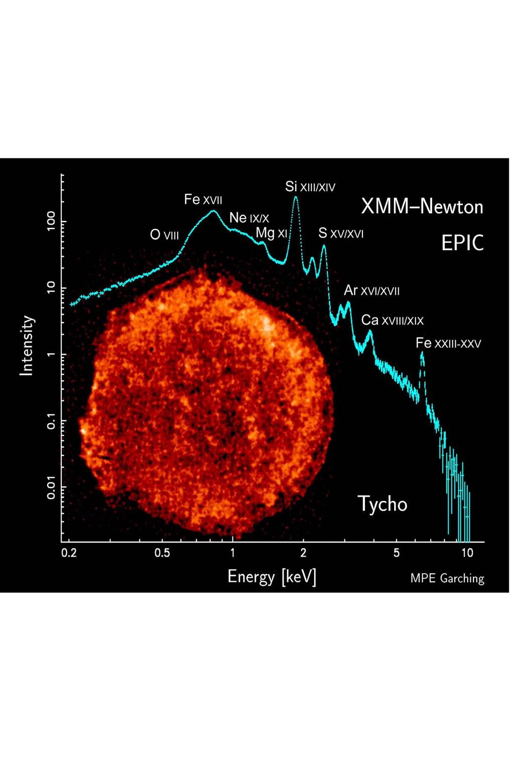
 extp meeting (extp: enhanced X-ray Timing and Polarization mission) Shanghai, 30th March 1st April 2016 MPE's views on SDDs as focal plane detectors for SFA - Overview: MPE HEG space projects XMM-Newton
Active Pixel Matrix for X-ray Satellite Missions
 Active Pixel Matrix for X-ray Satellite Missions P. Holl 1,*, P. Fischer 2, P. Klein 3, G. Lutz 4, W. Neeser 2, L. Strüder 5, N. Wermes 2 1 Ketek GmbH, Am Isarbach 30, D-85764 Oberschleißheim, Germany
DELIVERABLE!D60.4! 1k!x!1k!pnCCD!Conceptual!Design! WP60!Advanced!Instrumentation!Development! 1 ST Reporting Period.
 www.solarnet-east.eu This project is supported by the European Commission s FP7 Capacities Programme for the period April 2013 - March 2017 under the Grant Agreement number 312495. DELIVERABLED60.4 1kx1kpnCCDConceptualDesign
Pixel hybrid photon detectors
 Pixel hybrid photon detectors for the LHCb-RICH system Ken Wyllie On behalf of the LHCb-RICH group CERN, Geneva, Switzerland 1 Outline of the talk Introduction The LHCb detector The RICH 2 counter Overall
Detectors for AXIS. Eric D. Miller Catherine Grant (MIT)
") Detectors for AXIS Eric D. Miller Catherine Grant (MIT) Outline detector technology and capabilities CCD (charge coupled device) APS (active pixel sensor) notional AXIS detector background particle environment
Detectors for AXIS Eric D. Miller Catherine Grant (MIT) Outline detector technology and capabilities CCD (charge coupled device) APS (active pixel sensor) notional AXIS detector background particle environment
Wide Field Imager for Athena
 Exploring the Hot and Energetic Universe: The first scientific conference dedicated to the Athena X-ray observatory Wide Field Imager for Athena Norbert Meidinger on behalf of the WFI proto-consortium
Simulation of High Resistivity (CMOS) Pixels
 Pixels") Simulation of High Resistivity (CMOS) Pixels Stefan Lauxtermann, Kadri Vural Sensor Creations Inc. AIDA-2020 CMOS Simulation Workshop May 13 th 2016 OUTLINE 1. Definition of High Resistivity Pixel Also
Simulation of High Resistivity (CMOS) Pixels Stefan Lauxtermann, Kadri Vural Sensor Creations Inc. AIDA-2020 CMOS Simulation Workshop May 13 th 2016 OUTLINE 1. Definition of High Resistivity Pixel Also
Multi-Element Si Sensor with Readout ASIC for EXAFS Spectroscopy 1
 Multi-Element Si Sensor with Readout ASIC for EXAFS Spectroscopy 1 Gianluigi De Geronimo a, Paul O Connor a, Rolf H. Beuttenmuller b, Zheng Li b, Antony J. Kuczewski c, D. Peter Siddons c a Microelectronics
Lecture 2. Part 2 (Semiconductor detectors =sensors + electronics) Segmented detectors with pn-junction. Strip/pixel detectors
 Segmented detectors with pn-junction. Strip/pixel detectors") Lecture 2 Part 1 (Electronics) Signal formation Readout electronics Noise Part 2 (Semiconductor detectors =sensors + electronics) Segmented detectors with pn-junction Strip/pixel detectors Drift detectors
Lecture 2 Part 1 (Electronics) Signal formation Readout electronics Noise Part 2 (Semiconductor detectors =sensors + electronics) Segmented detectors with pn-junction Strip/pixel detectors Drift detectors
The Wide-Field Imager for IXO: Status and future activities
 The Wide-Field Imager for IXO: Status and future activities The MIT Faculty has made this article openly available. Please share how this access benefits you. Your story matters. Citation As Published
The Simbol-X focal plane
 Mem. S.A.It. Vol. 79, 32 c SAIt 2008 Memorie della The Simbol-X focal plane P. Laurent 1,4, P. Lechner 2, M. Authier 1, U. Briel 3, C. Cara 1, S. Colonges 4, P. Ferrando 1,4, J. Fontignie 1, E. Kendziorra
Semiconductor Detector Systems
 Semiconductor Detector Systems Helmuth Spieler Physics Division, Lawrence Berkeley National Laboratory OXFORD UNIVERSITY PRESS ix CONTENTS 1 Detector systems overview 1 1.1 Sensor 2 1.2 Preamplifier 3
DepFET detectors in astrophysics and particle physics instrumentation (and photon science)
") Jelena Ninkovic 1 607. WE Heraeus-Seminar, Feb. 2016 DepFET detectors in astrophysics and particle physics instrumentation (and photon science) Jelena Ninkovic for the MPG HLL team MPS Semiconductor Laboratory,
Jelena Ninkovic 1 607. WE Heraeus-Seminar, Feb. 2016 DepFET detectors in astrophysics and particle physics instrumentation (and photon science) Jelena Ninkovic for the MPG HLL team MPS Semiconductor Laboratory,
Today s Outline - January 25, C. Segre (IIT) PHYS Spring 2018 January 25, / 26
 PHYS Spring 2018 January 25, / 26") Today s Outline - January 25, 2018 C. Segre (IIT) PHYS 570 - Spring 2018 January 25, 2018 1 / 26 Today s Outline - January 25, 2018 HW #2 C. Segre (IIT) PHYS 570 - Spring 2018 January 25, 2018 1 / 26 Today
Today s Outline - January 25, 2018 C. Segre (IIT) PHYS 570 - Spring 2018 January 25, 2018 1 / 26 Today s Outline - January 25, 2018 HW #2 C. Segre (IIT) PHYS 570 - Spring 2018 January 25, 2018 1 / 26 Today
pcvd diamond beam position monitors for PETRA III
 pcvd diamond beam position monitors for PETRA III Eckhard Wörner Diamond Materials GmbH Tullastraße 72, 79108 Freiburg, Germany CARAT workshop 13-15.12.09 1/39 Outline Some news about Diamond Materials
Strip Detectors. Principal: Silicon strip detector. Ingrid--MariaGregor,SemiconductorsasParticleDetectors. metallization (Al) p +--strips
 p +--strips") Strip Detectors First detector devices using the lithographic capabilities of microelectronics First Silicon detectors -- > strip detectors Can be found in all high energy physics experiments of the last
Strip Detectors First detector devices using the lithographic capabilities of microelectronics First Silicon detectors -- > strip detectors Can be found in all high energy physics experiments of the last
Production of HPDs for the LHCb RICH Detectors
 Production of HPDs for the LHCb RICH Detectors LHCb RICH Detectors Hybrid Photon Detector Production Photo Detector Test Facilities Test Results Conclusions IEEE Nuclear Science Symposium Wyndham, 24 th
Nuclear Instruments and Methods in Physics Research A
 Nuclear Instruments and Methods in Physics Research A 624 () 5 547 Contents lists available at ScienceDirect Nuclear Instruments and Methods in Physics Research A journal homepage: www.elsevier.com/locate/nima
 http://clicdp.cern.ch Hybrid Pixel Detectors with Active-Edge Sensors for the CLIC Vertex Detector Simon Spannagel on behalf of the CLICdp Collaboration Experimental Conditions at CLIC CLIC beam structure
Photon Diagnostics. FLASH User Workshop 08.
 Photon Diagnostics FLASH User Workshop 08 Kai.Tiedtke@desy.de Outline What kind of diagnostic tools do user need to make efficient use of FLASH? intensity (New GMD) beam position intensity profile on the
On-line spectrometer for FEL radiation at
 On-line spectrometer for FEL radiation at FERMI@ELETTRA Fabio Frassetto 1, Luca Poletto 1, Daniele Cocco 2, Marco Zangrando 3 1 CNR/INFM Laboratory for Ultraviolet and X-Ray Optical Research & Department
The European XFEL: a great opportunity for science, a challenge for detectors!
 The European XFEL: a great opportunity for science, a challenge for detectors! Guillaume Potdevin Photon Science Detector Systems DESY- Hamburg; Germany Outlook The European XFEL Introduction General informations
CCD47-10 NIMO Back Illuminated Compact Pack High Performance CCD Sensor
 CCD47-10 NIMO Back Illuminated Compact Pack High Performance CCD Sensor FEATURES 1024 by 1024 Nominal (1056 by 1027 Usable Pixels) Image area 13.3 x 13.3mm Back Illuminated format for high quantum efficiency
The High-Voltage Monolithic Active Pixel Sensor for the Mu3e Experiment
 The High-Voltage Monolithic Active Pixel Sensor for the Mu3e Experiment Shruti Shrestha On Behalf of the Mu3e Collaboration International Conference on Technology and Instrumentation in Particle Physics
The Wide Field Imager for the Athena X-ray Observatory
 Wide Field Imager The for the Athena X-ray Observatory Arne Rau (Athena/WFI Project Scien:st, MPE - on behalf of the WFI Team) The Hot and Energetic Universe - Science Theme for ESA s L2 Mission How do
DESIGN AND MEASUREMENT WITH A NEW PORTABLE X-RAY CAMERA FOR FULL-FIELD FLUORESCENCE IMAGING
 14 DESIGN AND MEASUREMENT WITH A NEW PORTABLE X-RAY CAMERA FOR FULL-FIELD FLUORESCENCE IMAGING I. Ordavo 1,2, A. Bjeoumikhov 3, S. Bjeoumikhova 3, G. Buzanich 4, R. Gubzhokov 4, R. Hartmann 1, S. Ihle
The 2D X-ray detector development program for the European XFEL
 The 2D X-ray detector development program for the European DESY-Photon Science Detector Group WorkPackage Detectors for Where is the challenge? 100 ms 100 ms 0.6 ms 200 ns 99.4 ms X-ray photons
Dynamic Range. Can I look at bright and faint things at the same time?
 Detector Basics The purpose of any detector is to record the light collected by the telescope. All detectors transform the incident radiation into a some other form to create a permanent record, such as
STA1600LN x Element Image Area CCD Image Sensor
 ST600LN 10560 x 10560 Element Image Area CCD Image Sensor FEATURES 10560 x 10560 Photosite Full Frame CCD Array 9 m x 9 m Pixel 95.04mm x 95.04mm Image Area 100% Fill Factor Readout Noise 2e- at 50kHz
Detector development activities at DESY FS-DS. Julian Becker Photon Science Detector Group, DESY
 Detector development activities at DESY FS-DS Julian Becker Photon Science Detector Group, DESY Overview >Introduction to our group: DESY FS-DS >Projects for synchrotron radiation detectors LAMBDA High-Z
VII. IR Arrays & Readout VIII.CCDs & Readout. This lecture course follows the textbook Detection of
 Detection of Light VII. IR Arrays & Readout VIII.CCDs & Readout This lecture course follows the textbook Detection of Light 4-3-2016 by George Rieke, Detection Cambridge of Light Bernhard Brandl University
Fast Solar Polarimeter
 Fast Solar Polarimeter A. Feller, F. Iglesias, K. Nagaraju, S. K. Solanki Max Planck Institute for Solar System Research and colleagues from the Max Planck semiconductor lab A. Feller FSP IAUS 305 1 /
CCDS. Lesson I. Wednesday, August 29, 12
 CCDS Lesson I CCD OPERATION The predecessor of the CCD was a device called the BUCKET BRIGADE DEVICE developed at the Phillips Research Labs The BBD was an analog delay line, made up of capacitors such
An Introduction to CCDs. The basic principles of CCD Imaging is explained.
 An Introduction to CCDs. The basic principles of CCD Imaging is explained. Morning Brain Teaser What is a CCD? Charge Coupled Devices (CCDs), invented in the 1970s as memory devices. They improved the
The Wide Field Imager Instrument for Athena
 The Wide Field Imager Instrument for Athena Norbert Meidinger a, Josef Eder a, Tanja Eraerds a, Kirpal Nandra a, Daniel Pietschner a, Markus Plattner a, Arne Rau a, and Rafael Strecker a a Max-Planck-Institut
Highly Miniaturised Radiation Monitor (HMRM) Status Report. Yulia Bogdanova, Nicola Guerrini, Ben Marsh, Simon Woodward, Rain Irshad
 Status Report. Yulia Bogdanova, Nicola Guerrini, Ben Marsh, Simon Woodward, Rain Irshad") Highly Miniaturised Radiation Monitor (HMRM) Status Report Yulia Bogdanova, Nicola Guerrini, Ben Marsh, Simon Woodward, Rain Irshad HMRM programme aim Aim of phase A/B: Develop a chip sized prototype radiation
Highly Miniaturised Radiation Monitor (HMRM) Status Report Yulia Bogdanova, Nicola Guerrini, Ben Marsh, Simon Woodward, Rain Irshad HMRM programme aim Aim of phase A/B: Develop a chip sized prototype radiation
Next generation microprobes: Detector Issues and Approaches
 Next generation microprobes: Detector Issues and Approaches D. Peter Siddons National Synchrotron Light Source Brookhaven National Laboratory Upton, New York 11973 USA. Outline Why do we need new detectors?
Based on lectures by Bernhard Brandl
 Astronomische Waarneemtechnieken (Astronomical Observing Techniques) Based on lectures by Bernhard Brandl Lecture 10: Detectors 2 1. CCD Operation 2. CCD Data Reduction 3. CMOS devices 4. IR Arrays 5.
arxiv:physics/ v1 [physics.acc-ph] 25 Apr 2000
![arxiv:physics/ v1 [physics.acc-ph] 25 Apr 2000](/thumbs/94/119571821.jpg "arxiv:physics/ v1 [physics.acc-ph] 25 Apr 2000") DESY -65 April 2 physics/463 arxiv:physics/463v1 [physics.acc-ph] 25 Apr 2 Test Results on the Silicon Pixel Detector for the TTF-FEL Beam Trajectory Monitor S. Hillert a, R. Ischebeck b, U. C. Müller
DESY -65 April 2 physics/463 arxiv:physics/463v1 [physics.acc-ph] 25 Apr 2 Test Results on the Silicon Pixel Detector for the TTF-FEL Beam Trajectory Monitor S. Hillert a, R. Ischebeck b, U. C. Müller
Chromatic X-Ray imaging with a fine pitch CdTe sensor coupled to a large area photon counting pixel ASIC
 Chromatic X-Ray imaging with a fine pitch CdTe sensor coupled to a large area photon counting pixel ASIC R. Bellazzini a,b, G. Spandre a*, A. Brez a, M. Minuti a, M. Pinchera a and P. Mozzo b a INFN Pisa
Where detectors are used in science & technology
 Lecture 9 Outline Role of detectors Photomultiplier tubes (photoemission) Modulation transfer function Photoconductive detector physics Detector architecture Where detectors are used in science & technology
X-ray Detectors: What are the Needs?
 X-ray Detectors: What are the Needs? Sol M. Gruner Physics Dept. & Cornell High Energy Synchrotron Source (CHESS) Ithaca, NY 14853 smg26@cornell.edu 1 simplified view of the Evolution of Imaging Synchrotron
X-ray FEL Oscillator (XFEL-O) Gun Requirements and R&D Overview FLS2010: WG5: High Brightness Guns March 1, 2010
 Gun Requirements and R&D Overview FLS2010: WG5: High Brightness Guns March 1, 2010") X-ray FEL Oscillator (XFEL-O) Gun Requirements and R&D Overview FLS2010: WG5: High Brightness Guns March 1, 2010 Nick Sereno (APS/ASD) - Argonne National Laboratory (ANL) / Advanced Photon source (APS)
X-ray FEL Oscillator (XFEL-O) Gun Requirements and R&D Overview FLS2010: WG5: High Brightness Guns March 1, 2010 Nick Sereno (APS/ASD) - Argonne National Laboratory (ANL) / Advanced Photon source (APS)
Characterization of the eline ASICs in prototype detector systems for LCLS
 Characterization of the eline ASICs in prototype detector systems for LCLS G. A Carini *, A. Dragone, B.-L. Berube, P. Caragiulo, D. M. Fritz, P. A. Hart, R. Herbst, S. Herrmann, C. J. Kenney, A. J. Kuczewski,
Demonstration of exponential growth and saturation at VUV wavelengths at the TESLA Test Facility Free-Electron Laser. P. Castro for the TTF-FEL team
 Demonstration of exponential growth and saturation at VUV wavelengths at the TESLA Test Facility Free-Electron Laser P. Castro for the TTF-FEL team 100 nm 1 Å FEL radiation TESLA Test Facility at DESY
Implementation of A Nanosecond Time-resolved APD Detector System for NRS Experiment in HEPS-TF
 Implementation of A Nanosecond Time-resolved APD Detector System for NRS Experiment in HEPS-TF LI Zhen-jie a ; MA Yi-chao c ; LI Qiu-ju a ; LIU Peng a ; CHANG Jin-fan b ; ZHOU Yang-fan a * a Beijing Synchrotron
Wide field imager instrument for the Advanced Telescope for High Energy Astrophysics
 Wide field imager instrument for the Advanced Telescope for High Energy Astrophysics Norbert Meidinger Kirpal Nandra Markus Plattner Matteo Porro Arne Rau Andrea Santangelo Chris Tenzer Jörn Wilms Journal
JUNGFRAU: a pixel detector for photon science at free electron laser facilities.
 WIR SCHAFFEN WISSEN HEUTE FÜR MORGEN Aldo Mozzanica for the Swiss Light Source Detector Group JUNGFRAU: a pixel detector for photon science at free electron laser facilities. PIXEL 2016 Outline Introduction
Instruction manual and data sheet ipca h
 1/15 instruction manual ipca-21-05-1000-800-h Instruction manual and data sheet ipca-21-05-1000-800-h Broad area interdigital photoconductive THz antenna with microlens array and hyperhemispherical silicon
ITk silicon strips detector test beam at DESY
 ITk silicon strips detector test beam at DESY Lucrezia Stella Bruni Nikhef Nikhef ATLAS outing 29/05/2015 L. S. Bruni - Nikhef 1 / 11 Qualification task I Participation at the ITk silicon strip test beams
3 General layout of the XFEL Facility
 3 General layout of the XFEL Facility 3.1 Introduction The present chapter provides an overview of the whole European X-Ray Free-Electron Laser (XFEL) Facility layout, enumerating its main components and
THz Pump Beam for LCLS. Henrik Loos. LCLS Hard X-Ray Upgrade Workshop July 29-31, 2009
 Beam for LCLS Henrik Loos Workshop July 29-31, 29 1 1 Henrik Loos Overview Coherent Radiation Sources Timing THz Source Performance 2 2 Henrik Loos LCLS Layout 6 MeV 135 MeV 25 MeV 4.3 GeV 13.6 GeV σ z.83
LCLS project update. John Arthur. LCLS Photon Systems Manager
 LCLS project update LCLS Photon Systems Manager LCLS major construction nearly finished Technical systems turning on with good performance Experimental instruments Expectations for early operation First
X-ray generation by femtosecond laser pulses and its application to soft X-ray imaging microscope
 X-ray generation by femtosecond laser pulses and its application to soft X-ray imaging microscope Kenichi Ikeda 1, Hideyuki Kotaki 1 ' 2 and Kazuhisa Nakajima 1 ' 2 ' 3 1 Graduate University for Advanced
CCD30-11 NIMO Back Illuminated Deep Depleted High Performance CCD Sensor
 CCD30-11 NIMO Back Illuminated Deep Depleted High Performance CCD Sensor FEATURES 1024 by 256 Pixel Format 26µm Square Pixels Image area 26.6 x 6.7mm Back Illuminated format for high quantum efficiency
The Hot and Energetic Universe
 The Hot and Energetic Universe An Athena+ supporting paper The Wide Field Imager (WFI) for Athena+ Authors and contributors A. Rau, N. Meidinger, K. Nandra, M. Porro, D. Barret, A. Santangelo, C. Schmid,
Introduction to X-ray Detectors for Synchrotron Radiation Applications
 Introduction to X-ray Detectors for Synchrotron Radiation Applications Pablo Fajardo Instrumentation Services and Development Division ESRF, Grenoble EIROforum School on Instrumentation (ESI 2011) Outline
Silicon Drift Detector. with On- Chip Ele ctronics for X-Ray Spectroscopy. KETEK GmbH Am Isarbach 30 D O berschleißheim GERMANY
 KETEK GmbH Am Isarbach 30 D-85764 O berschleißheim GERMANY Silicon Drift Detector Phone +49 (0)89 315 57 94 Fax +49 (0)89 315 58 16 with On- Chip Ele ctronics for X-Ray Spectroscopy high energy resolution
The Medipix3 Prototype, a Pixel Readout Chip Working in Single Photon Counting Mode with Improved Spectrometric Performance
 26 IEEE Nuclear Science Symposium Conference Record NM1-6 The Medipix3 Prototype, a Pixel Readout Chip Working in Single Photon Counting Mode with Improved Spectrometric Performance R. Ballabriga, M. Campbell,
CMOS Detectors Ingeniously Simple!
 CMOS Detectors Ingeniously Simple! A.Schöning University Heidelberg B-Workshop Neckarzimmern 18.-20.2.2015 1 Detector System on Chip? 2 ATLAS Pixel Module 3 ATLAS Pixel Module MCC sensor FE-Chip FE-Chip
Nonintercepting Diagnostics for Transverse Beam Properties: from Rings to ERLs
 Nonintercepting Diagnostics for Transverse Beam Properties: from Rings to ERLs Alex H. Lumpkin Accelerator Operations Division Advanced Photon Source Presented at Jefferson National Accelerator Laboratory
Electron-Bombarded CMOS
 New Megapixel Single Photon Position Sensitive HPD: Electron-Bombarded CMOS University of Lyon / CNRS-IN2P3 in collaboration with J. Baudot, E. Chabanat, P. Depasse, W. Dulinski, N. Estre, M. Winter N56:
Digital camera. Sensor. Memory card. Circuit board
 Digital camera Circuit board Memory card Sensor Detector element (pixel). Typical size: 2-5 m square Typical number: 5-20M Pixel = Photogate Photon + Thin film electrode (semi-transparent) Depletion volume
Progress of the TEO experiment at FLASH
 Progress of the TEO experiment at VUV-FEL at DESY - Armin Azima S. Duesterer, J. Feldhaus, H. Schlarb, H. Redlin, B. Steffen, DESY Hamburg K. Sengstock, Uni Hamburg Adrian Cavalieri, David Fritz, David
Introduction. Chapter 1
 1 Chapter 1 Introduction During the last decade, imaging with semiconductor devices has been continuously replacing conventional photography in many areas. Among all the image sensors, the charge-coupled-device
CSPADs: how to operate them, which performance to expect and what kind of features are available
 CSPADs: how to operate them, which performance to expect and what kind of features are available Gabriella Carini, Gabriel Blaj, Philip Hart, Sven Herrmann Cornell-SLAC Pixel Array Detector What is it?
Moderne Teilchendetektoren - Theorie und Praxis 2. Dr. Bernhard Ketzer Technische Universität München SS 2013
 Moderne Teilchendetektoren - Theorie und Praxis 2 Dr. Bernhard Ketzer Technische Universität München SS 2013 7 Signal Processing and Acquisition 7.1 Signals 7.2 Amplifier 7.3 Electronic Noise 7.4 Analog-to-Digital
A flexible compact readout circuit for SPAD arrays ABSTRACT Keywords: 1. INTRODUCTION 2. THE SPAD 2.1 Operation 7780C - 55
 A flexible compact readout circuit for SPAD arrays Danial Chitnis * and Steve Collins Department of Engineering Science University of Oxford Oxford England OX13PJ ABSTRACT A compact readout circuit that
X-Ray Transport, Diagnostic, & Commissioning Plans. LCLS Diagnostics and Commissioning Workshop
 X-Ray Transport, Diagnostic, & Commissioning Plans LCLS Diagnostics and Commissioning Workshop *This work was performed under the auspices of the U.S. Department of Energy by the University of California,
Light gathering Power: Magnification with eyepiece:
 Telescopes Light gathering Power: The amount of light that can be gathered by a telescope in a given amount of time: t 1 /t 2 = (D 2 /D 1 ) 2 The larger the diameter the smaller the amount of time. If
Water-Window Microscope Based on Nitrogen Plasma Capillary Discharge Source
 2015 International Workshop on EUV and Soft X-Ray Sources Water-Window Microscope Based on Nitrogen Plasma Capillary Discharge Source T. Parkman 1, M. F. Nawaz 2, M. Nevrkla 2, M. Vrbova 1, A. Jancarek
Gas Pixel Detectors. Ronaldo Bellazzini INFN - Pisa. 8th International Workshop on Radiation Imaging Detectors (IWORID-8) Pisa 2-6/july 2
 Pisa 2-6/july 2") Gas Pixel Detectors Ronaldo Bellazzini INFN - Pisa 8th International Workshop on Radiation Imaging Detectors (IWORID-8) Pisa 2-6/july 2 2006 Polarimetry: The Missing Piece of the Puzzle Imaging: Chandra
Gas Pixel Detectors Ronaldo Bellazzini INFN - Pisa 8th International Workshop on Radiation Imaging Detectors (IWORID-8) Pisa 2-6/july 2 2006 Polarimetry: The Missing Piece of the Puzzle Imaging: Chandra
LCLS Injector Diagnostics. Henrik Loos. Diagnostics overview Transverse Beam Properties Longitudinal Beam Properties
 Diagnostics overview Transverse Beam Properties Longitudinal Beam Properties LCLS Diagnostics Tasks Charge Toroids (Gun, Inj, BC, Und) Faraday cups (Gun & Inj) Trajectory & energy Stripline BPMs (Gun,
ELECTRON BEAM DIAGNOSTICS AND FEEDBACK FOR THE LCLS-II*
 THB04 Proceedings of FEL2014, Basel, Switzerland ELECTRON BEAM DIAGNOSTICS AND FEEDBACK FOR THE LCLS-II* Josef Frisch, Paul Emma, Alan Fisher, Patrick Krejcik, Henrik Loos, Timothy Maxwell, Tor Raubenheimer,
Fundamentals of CMOS Image Sensors
 CHAPTER 2 Fundamentals of CMOS Image Sensors Mixed-Signal IC Design for Image Sensor 2-1 Outline Photoelectric Effect Photodetectors CMOS Image Sensor(CIS) Array Architecture CIS Peripherals Design Considerations
ISIS2 as a Pixel Sensor for ILC
 ISIS2 as a Pixel Sensor for ILC Yiming Li (University of Oxford) on behalf of UK ISIS Collaboration (U. Oxford, RAL, Open University) LCWS 10 Beijing, 28th March 2010 1 / 24 Content Introduction to ISIS
1-Å FEL Oscillator with ERL Beams
 1-Å FEL Oscillator with ERL Beams 29 th International FEL Conference August 26-31, BINP Novosibirsk, Russia Kwang-Je Kim, ANL Sven Reiche, UCLA Yuri Shvyd ko, ANL FELs for λ
Development of Pixel Detectors for the Inner Tracker Upgrade of the ATLAS Experiment
 Development of Pixel Detectors for the Inner Tracker Upgrade of the ATLAS Experiment Natascha Savić L. Bergbreiter, J. Breuer, A. Macchiolo, R. Nisius, S. Terzo IMPRS, Munich # 29.5.215 Franz Dinkelacker
Ultra fast single photon counting chip
 Ultra fast single photon counting chip P. Grybos, P. Kmon, P. Maj, R. Szczygiel Faculty of Electrical Engineering, Automatics, Computer Science and Biomedical Engineering AGH University of Science and
Performance of the SASE3 monochromator equipped with a provisional short grating. Variable line spacing grating specifications
 TECHNICAL REPORT Performance of the SASE monochromator equipped with a provisional short grating. Variable line spacing grating specifications N. Gerasimova for the X-Ray Optics and Beam Transport group
LCLS-II-HE Instrumentation
 LCLS-II-HE Instrumentation Average Brightness (ph/s/mm 2 /mrad 2 /0.1%BW) LCLS-II-HE: Enabling New Experimental Capabilities Structural Dynamics at the Atomic Scale Expand the photon energy reach of LCLS-II
Chapter 4 Vertex. Qun Ouyang. Nov.10 th, 2017Beijing. CEPC detector CDR mini-review
 Chapter 4 Vertex Qun Ouyang Nov.10 th, 2017Beijing Nov.10 h, 2017 CEPC detector CDR mini-review CEPC detector CDR mini-review Contents: 4 Vertex Detector 4.1 Performance Requirements and Detector Challenges
Test Beam Measurements for the Upgrade of the CMS Phase I Pixel Detector
 Test Beam Measurements for the Upgrade of the CMS Phase I Pixel Detector Simon Spannagel on behalf of the CMS Collaboration 4th Beam Telescopes and Test Beams Workshop February 4, 2016, Paris/Orsay, France
Beam Diagnostics, Low Level RF and Feedback for Room Temperature FELs. Josef Frisch Pohang, March 14, 2011
 Beam Diagnostics, Low Level RF and Feedback for Room Temperature FELs Josef Frisch Pohang, March 14, 2011 Room Temperature / Superconducting Very different pulse structures RT: single bunch or short bursts
Characterisation of a CMOS Charge Transfer Device for TDI Imaging
 Preprint typeset in JINST style - HYPER VERSION Characterisation of a CMOS Charge Transfer Device for TDI Imaging J. Rushton a, A. Holland a, K. Stefanov a and F. Mayer b a Centre for Electronic Imaging,
Integration of Optoelectronic and RF Devices for Applications in Optical Interconnect and Wireless Communication
 Integration of Optoelectronic and RF Devices for Applications in Optical Interconnect and Wireless Communication Zhaoran (Rena) Huang Assistant Professor Department of Electrical, Computer and System Engineering