Detector development activities at DESY FS-DS. Julian Becker Photon Science Detector Group, DESY
|
|
|
- Jewel Charles
- 5 years ago
- Views:
Transcription


1 Detector development activities at DESY FS-DS Julian Becker Photon Science Detector Group, DESY
2 Overview >Introduction to our group: DESY FS-DS >Projects for synchrotron radiation detectors LAMBDA High-Z pixel detectors (hard X-ray detectors) PERCIVAL >Project for the European XFEL AGIPD J. Becker DESY/KEK meeting 20/03/12 Page 2


3 Our group: DESY FS-DS Heinz Graafsma Group leader Stephanie Jack Project manager Michael Lohmann Detector scientist Trixi Wunderer Detector scientist Ulrich Trunk Detector scientist David Pennicard Postdoc Laura Bianco Postdoc Julian Becker Postdoc Alessandro Marras Postdoc Alexander Kluyev Engineer-physicist Sabine Lange Electronic engineer Sergej Smoljanin Electronic technician Helmut Hirsemann Mechanical engineer Matthias Bayer Mechanical engineer J. Becker DESY/KEK meeting 20/03/12 Page 3 Björn Nilsson Mechanical technician
4 Our detector development projects (all collaborations) > LAMBDA (Large Area Medipix3-Based Detector Array) Photon counting pixel detector module > High-Z detectors (Ge, HiZpad collaboration, GALAPAD) New semiconductor pixel detectors for hard X-rays > PERCIVAL (Pixelated Energy Resolving CMOS Imager, Versatile And Large) Low E (250 ev 1 kev) imaging detector > AGIPD (Adaptive Gain Integrating Pixel Detector) 2D detector for XFEL, developed with PSI, Uni Hamburg, Uni Bonn > DSSC (DEPMOS Sensor with Signal Compression) XFEL detector project, led by MPI-HLL, Munich J. Becker DESY/KEK meeting 20/03/12 Page 4
5 Other involvements > CAMP (CFEL-ASG Multi-Purpose) Chamber Already in use at LCLS > Detector and science simulation (HORUS) > XNAP (2D array of avalanche photodiodes) Collaboration with ESRF, U. Heidelberg, SPring-8, Exelitas > Diamond beam position monitors with RF readout Collaboration with ESRF > Detector loan pool Pool of a variety of detectors (Pilatus, Maxipix, CCDs, imaging plates, etc.) and associated equipment to support user operation at photon sources. J. Becker DESY/KEK meeting 20/03/12 Page 5
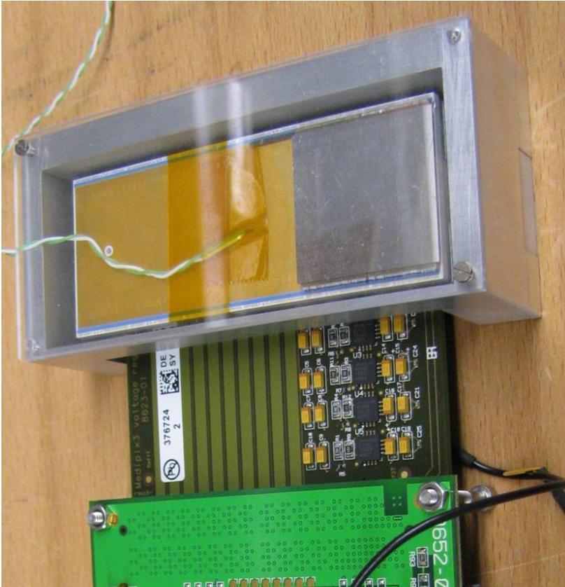
6 Hybrid pixel detectors (counting) > Pixellated photodiode sensor > Readout chip with 1 readout channel per pixel 14 mm Medipix3 chip J. Becker DESY/KEK meeting 20/03/12 Page 6
 > 256 * 256 pixels, 55µm > 2 counters per pixel for deadtime-free readout Up to 2000 fps")

7 Medipix3 readout chip > 21 groups in collaboration Chip design at CERN > Successor to Medipix2 (Maxipix) > 256 * 256 pixels, 55µm > 2 counters per pixel for deadtime-free readout Up to 2000 fps with 12 bit counter depth > Charge summing circuitry to compensate charge sharing effects Charge shared between pixels More reliable hit detection Better energy discrimination J. Becker DESY/KEK meeting 20/03/12 Page 7
 Maxipix (ESRF, Medipix2; 55µm pixels) > Advantages Single photon counting ( noise free ) Fast")
 Poor efficiency at high energies Problems at high flux rates J.")
8 Hybrid pixels and X-ray detection > First generation of X-ray hybrid pixels in use Pilatus (Dectris, PSI; 172 µm pixels) Maxipix (ESRF, Medipix2; 55µm pixels) > Advantages Single photon counting ( noise free ) Fast readout Large dynamic range Energy discrimination > Disadvantages Pixel-to-pixel variation in electronics (must be calibrated) Poor efficiency at high energies Problems at high flux rates J. Becker DESY/KEK meeting 20/03/12 Page 8
 Si has poor absorption efficiency > 20 kev Heavier semiconductors (Ge, CdTe, GaAs) allow hard X-ray detection > PERCIVAL (Pixelated Energy Resolving CMOS Imager,")
9 Detector developments at DESY > LAMBDA (Large Area Medipix-Based Detector Array) Large detector modules using new Medipix3 chip 55µm pixel size, fast readout, greater functionality > High-Z semiconductors (Ge, HiZpad, GALAPAD) Si has poor absorption efficiency > 20 kev Heavier semiconductors (Ge, CdTe, GaAs) allow hard X-ray detection > PERCIVAL (Pixelated Energy Resolving CMOS Imager, Versatile And Large) Low E (250 ev 1 kev) CMOS detector with 25 µm pixel size Designed by STFC, readout by DESY > AGIPD (Adaptive Gain Integrating Pixel Detector) Integrating detector with dynamic gain switching In-pixel storage for ultra fast (4.5 MHz) imaging at XFEL J. Becker DESY/KEK meeting 20/03/12 Page 9


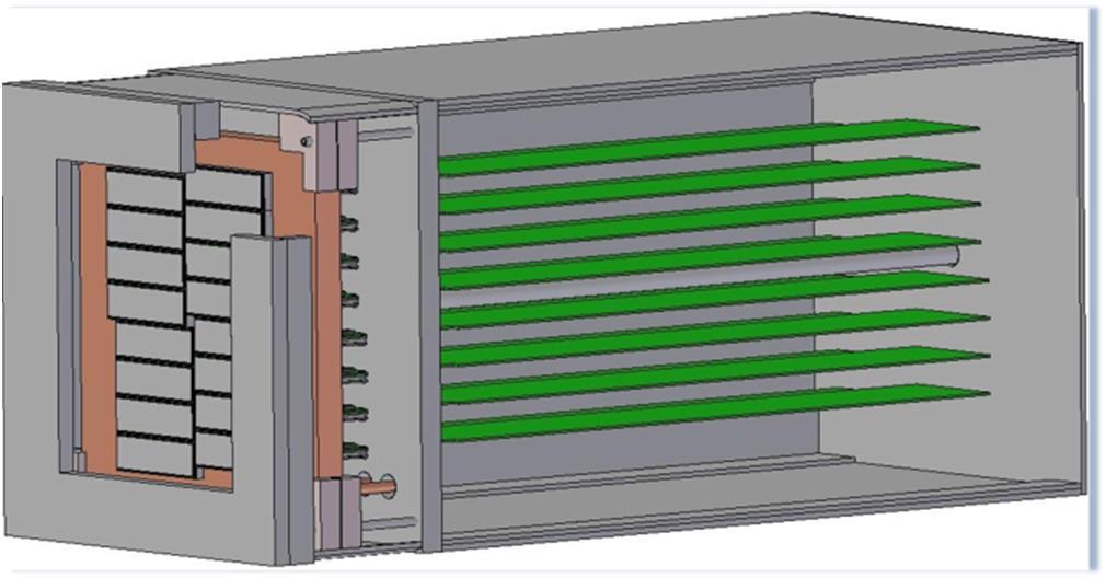
10 LAMBDA detector head > Large sensor area 2-by-6-chip layout 1536*512 pixel, 84 mm * 28 mm Set by typical silicon and high-z wafer sizes (6, 3 ) > Suitable for high-speed readout > Low-temp operation possible > Modular design Multiple readout chips build a single module Multiple modules tiled in large system 1 large Si sensor 84 mm * 28 mm 500-pin high density connector or 2 hexa high-z sensors Each 42 mm * 28 mm Voltage reg. board J. Becker DESY/KEK meeting 20/03/12 Page 10
 > Mechanics with Peltier cooling >")
 > Prototype readout board (completed) USB2")
 > High-speed readout Common")

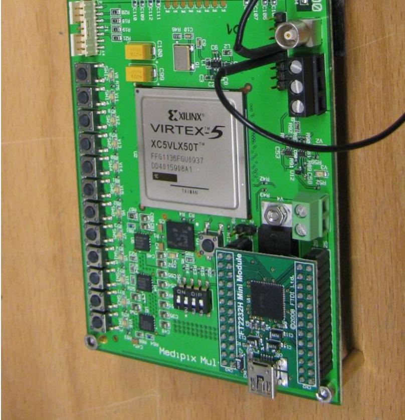
11 First prototype systems > 4 modules built with quad sensors (2*2 chip, 512*512 pixels) > Mechanics with Peltier cooling > Electronics to one side of sensor (but right-angle connector now available) > Prototype readout board (completed) USB2 communication with control PC (10 frames per second with large-area sensor should be possible) > High-speed readout Common readout mezzanine board being developed for LAMBDA, PERCIVAL and AGIPD Multiple 10 Gigabit Ethernet links for full-speed readout J. Becker DESY/KEK meeting 20/03/12 Page 11


12 Test results so far > Quad detectors are functional > Full-size sensor currently being bump-bonded at IZM > Working on high-speed readout J. Becker DESY/KEK meeting 20/03/12 Page 12
13 High-Z materials X-ray absorption efficiency > Replacing Si with high-z material could combine hybrid pixel advantages with high efficiency with hard X-rays > However, each high-z material has its downsides! > Our projects: Proportion absorbed / interacting 120% 100% 80% 60% 40% 20% 0% X-ray absorption / interaction Silicon (500um) Ge / GaAs (500um) CdTe (500um) X-ray energy (kev) Germanium development with Canberra and IZM (Berlin) Cadmium Telluride HiZPAD consortium (led by ESRF) Gallium Arsenide Russian-German partnership with FMF, KIT, JINR (Dubna) and RID Ltd. (Tomsk) MAR345 ~2% at 100keV J. Becker DESY/KEK meeting 20/03/12 Page 13
")

 J.")
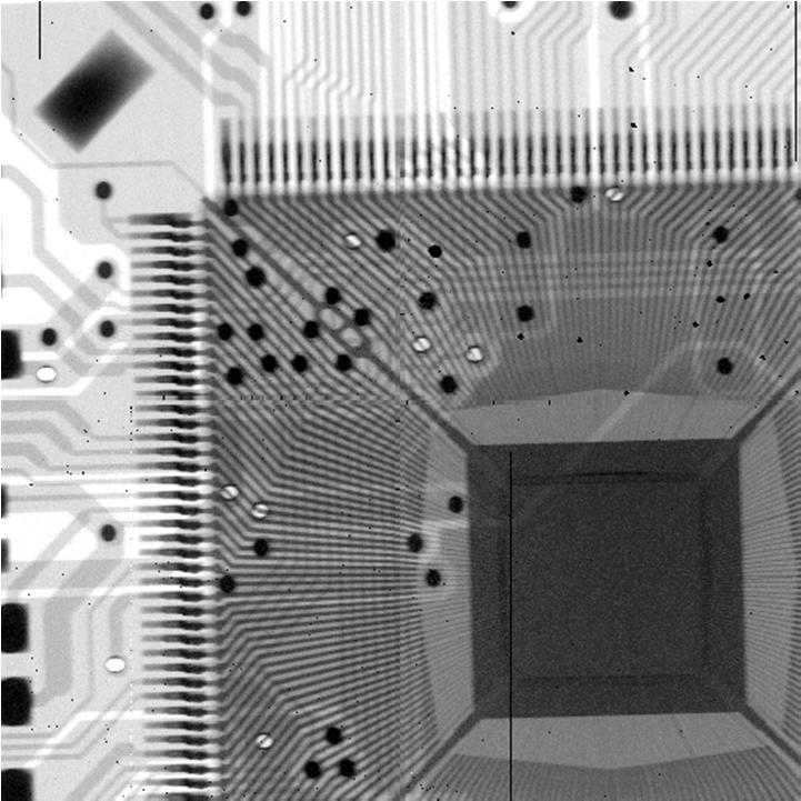
14 Germanium sensor production and bump bonding > Sensor structure (Canberra) Modification of existing strip detector technology 55µm pixels, 700 µm thick > Indium bump bonding (IZM) Sensor and ASIC bonded at T < 100 C During cooling, ductility of Indium compensates for mismatch in contraction > 2 high purity Ge wafers plus mechanical dummies received from Canberra 16 Medipix3 singles / wafer IZM optimizing process using dummies HP Ge bonding follows soon > Readout and mechanics by DESY (LAMBDA framework) J. Becker DESY/KEK meeting 20/03/12 Page 14
 > CdTe (Z Cd,Te = 48, 52,")
, often with inhomogeneities > Tested CdTe sensor with Medipix2")
 J.")
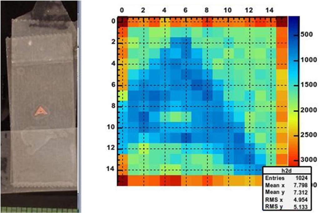
15 Cadmium Telluride > HiZPAD (High-Z sensors for Pixel Array Detectors) EU-funded consortium 12 institutes (led by ESRF) > CdTe (Z Cd,Te = 48, 52, Z Si = 14) Already used in single-element detectors / small arrays Small wafers (3 ), often with inhomogeneities > Tested CdTe sensor with Medipix2 readout 55µm pixel, 256 * 256 array, 1000 µm thick Tests done at DORIS III - BW5 beam line (160 kev photons) J. Becker DESY/KEK meeting 20/03/12 Page 15
16 PERCIVAL project photodiodes embedded circuitry e- backthinned (~12um) epi Si handling wafer board Aspired performance parameters: Primary energy range 250 ev 1 kev(will work from <200 evto few kev) 12 µm Si sensitive volume with 25 µm pixels 4k 4k pixel sensor 4 sensors in cloverleaf arrangement can make up 64 Mpixel(20cm x 20cm) back-illuminated, back-thinned for uniform QE > 90% 120 Hz frame rate and lower 2-side buttable(space between active pixel edges on the order of 1mm) electronic noise < 15e-, full well ~ 20 Me- Multi-gain approach to access full dynamic range, all gains active all the time J. Becker DESY/KEK meeting 20/03/12 Page 16
17 Overview >Introduction to our group: DESY FS-DS >Projects for synchrotron radiation detectors LAMBDA High-Z pixel detectors (hard X-ray detectors) PERCIVAL >Project for the European XFEL AGIPD J. Becker DESY/KEK meeting 20/03/12 Page 17

 through FEL")


18 The European XFEL 17.5 GeV linear electron accelerator producing 12.4 kev x-rays (tunable) through FEL process unprecedented peak brilliance user facility: common infrastructure shared by many experiments Tunnel: 3.4 km long m deep DESY Switch Building (Osdorfer Born) Experimental Hall (Schenefeld) J. Becker DESY/KEK meeting 20/03/12 Page 18
19 Single shot imaging e.g. Coherent Diffractive Imaging (CDI or CXI): K. J. Gaffney and H. N. Chapman, Science 8 June 2007 J. Becker DESY/KEK meeting 20/03/12 Page 19

 pulse consists of 10 12 photons arriving <100 fs > Beam")
 nominal design energy for AGIPD J.")
20 XFEL pulse trains > Special structure of pulse trains: 600 µs long pulse trains at a repetition rate of 10 Hz Each train consists of 2700 pulses with a separation of 220 ns Each (SASE) pulse consists of photons arriving <100 fs > Beam energy: 5 25 kev (depends on station) 12.4 kev (λ=0.1 nm) nominal design energy for AGIPD J. Becker DESY/KEK meeting 20/03/12 Page 20
21 XFEL Detector requirements 4.5 MHz J. Becker DESY/KEK meeting 20/03/12 Page 21
 Reading out of single frames during pulse train")
22 XFEL challenges XFEL provides Simultaneous deposition of all photons Challenges Single photon counting not possible Dynamic range: 10 4 photons/pixel with single photon sensitivity Approach Charge integration Dynamic gain switching 3 gain stages Single photon sensitivity in highest gain High number of bunches 2700 bunches per train (600 µs) Reading out of single frames during pulse train impossible Analog memory in the pixel using the 350 storage cells per pixel J. Becker DESY/KEK meeting 20/03/12 Page 22
23 AGIPD ASIC Sensor ASIC per pixel Pixel matrix HV THR + - CDS SW CTRL DAC Analog Mem Analog Mem RO Amp RO bus (per column) Calibration circuitry Adaptive gain amplifier 352 analog memory cells ASIC periphery Chip output driver Mux J. Becker DESY/KEK meeting 20/03/12 Page 23


24 Imaging with AGIPD 0.2 prototype J. Becker DESY/KEK meeting 20/03/12 Page 24


25 The detector layout > Specifications: 1 Mpixel 4 quadrants 4 modules per quadrant 1 module: 8 x 2 chips, 1 chip: 64 x 64 pixels 8 chips 2 chips module single chip quadrant 200 x 200 µm 2 pixel size 500 µm silicon sensor Hole for direct beam Upgradable to 4 Mpix J. Becker DESY/KEK meeting 20/03/12 Page 25
26 Summary (of detector projects) > LAMBDA Large area modules (1536 * 512 pixels, 84 mm * 28 mm) 55 µm pixel size 2 khz frame rate > HiZ materials (Ge, GaAs, CdTe) Direct detection imaging at high energies Compatible with LAMBDA modules > PERCIVAL Low energy imaging (<250 ev to >1 kev) 25 µm pixel size 120 Hz frame rate > AGIPD 4.5 MHz imaging kev γ dynamic range single photon sensitivity for E > 5 kev J. Becker DESY/KEK meeting 20/03/12 Page 26
27 Backup J. Becker DESY/KEK meeting 20/03/12 Page 27
28 DAQ architecture custom 10 GE UDP 10 GE TCP TCP, FC, Infiniband DESY IT standard 2D pixel FEE Train builder PC layer C. Youngman, S. Esanov FEI Data cache net. switch switch.... PCs Archive silos 1D FEE FEI.... camera Train builder? PC layer Data cache FEI net. switch switch PCs PCs Front End Electronics (FEE) Front End Interface (FEI) interface to Train Builder integrated in 2D Train builder layer builds trains simple data processing PC layer interface to cache additional train building more complex data process Data cache hold, analyze, reduce and reject data post processing commit to silo J. Becker DESY/KEK meeting 20/03/12 Page 28
Detector Challenges in Photon Science.
 Detector Challenges in Photon Science. Heinz Graafsma DESY-Hamburg; Germany & University of Mid-Sweden Outline > Photon Science and the detector challenge > Synchrotron storage rings The LAMBDA system
The European XFEL: a great opportunity for science, a challenge for detectors!
 The European XFEL: a great opportunity for science, a challenge for detectors! Guillaume Potdevin Photon Science Detector Systems DESY- Hamburg; Germany Outlook The European XFEL Introduction General informations
The 2D X-ray detector development program for the European XFEL
 The 2D X-ray detector development program for the European DESY-Photon Science Detector Group WorkPackage Detectors for Where is the challenge? 100 ms 100 ms 0.6 ms 200 ns 99.4 ms X-ray photons
X-ray Detectors at DESY
 X-ray Detectors at DESY (Contribution given at the FEL2006 meeting in Berlin) DESY The European XFEL Time structure: difference with others Electron bunch trains; up to 3000 bunches in 600 μsec, repeated
AGIPD, a high dynamic range fast detector for the European XFEL
 Home Search Collections Journals About Contact us My IOPscience AGIPD, a high dynamic range fast detector for the European XFEL This content has been downloaded from IOPscience. Please scroll down to see
Large-Area CdTe Photon-Counting Pixel Detectors
 Large-Area CdTe Photon-Counting Pixel Detectors Tilman Donath, Application Scientist 22.6.2015, DIR2015, Ghent DECTRIS Ltd. 5400 Baden Switzerland www.dectris.com Agenda 1. Introduction Hybrid Photon Counting
Chromatic X-Ray imaging with a fine pitch CdTe sensor coupled to a large area photon counting pixel ASIC
 Chromatic X-Ray imaging with a fine pitch CdTe sensor coupled to a large area photon counting pixel ASIC R. Bellazzini a,b, G. Spandre a*, A. Brez a, M. Minuti a, M. Pinchera a and P. Mozzo b a INFN Pisa
Strip Detectors. Principal: Silicon strip detector. Ingrid--MariaGregor,SemiconductorsasParticleDetectors. metallization (Al) p +--strips
 p +--strips") Strip Detectors First detector devices using the lithographic capabilities of microelectronics First Silicon detectors -- > strip detectors Can be found in all high energy physics experiments of the last
Strip Detectors First detector devices using the lithographic capabilities of microelectronics First Silicon detectors -- > strip detectors Can be found in all high energy physics experiments of the last
 http://clicdp.cern.ch Hybrid Pixel Detectors with Active-Edge Sensors for the CLIC Vertex Detector Simon Spannagel on behalf of the CLICdp Collaboration Experimental Conditions at CLIC CLIC beam structure
LAMBDA Detector An Example of a State-of-the-Art Photon Counting Imaging System
 3 LAMBDA Detector An Example of a State-of-the-Art Photon Counting Imaging System David Pennicard, Julian Becker, and Milija Sarajlić CONTENTS 3.1 Introduction...56 3.1.1 State-of-the-Art Detectors at
X-ray Detectors: What are the Needs?
 X-ray Detectors: What are the Needs? Sol M. Gruner Physics Dept. & Cornell High Energy Synchrotron Source (CHESS) Ithaca, NY 14853 smg26@cornell.edu 1 simplified view of the Evolution of Imaging Synchrotron
AGIPD calibration status report
 AGIPD calibration status report A. Allahgholi 2, R. Dinapoli 1, P. Goettlicher 2, M. Gronewald 4, H. Graafsma 2,5, D. Greiffenberg 1, B.H. Henrich 1, H. Hirsemann 2, S. Jack 2, R. Klanner 3, A. Klyuev
The Medipix3 Prototype, a Pixel Readout Chip Working in Single Photon Counting Mode with Improved Spectrometric Performance
 26 IEEE Nuclear Science Symposium Conference Record NM1-6 The Medipix3 Prototype, a Pixel Readout Chip Working in Single Photon Counting Mode with Improved Spectrometric Performance R. Ballabriga, M. Campbell,
The High-Voltage Monolithic Active Pixel Sensor for the Mu3e Experiment
 The High-Voltage Monolithic Active Pixel Sensor for the Mu3e Experiment Shruti Shrestha On Behalf of the Mu3e Collaboration International Conference on Technology and Instrumentation in Particle Physics
MEASUREMENT OF TIMEPIX DETECTOR PERFORMANCE VICTOR GUTIERREZ DIEZ UNIVERSIDAD COMPLUTENSE DE MADRID
 MEASUREMENT OF TIMEPIX DETECTOR PERFORMANCE VICTOR GUTIERREZ DIEZ UNIVERSIDAD COMPLUTENSE DE MADRID ABSTRACT Recent advances in semiconductor technology allow construction of highly efficient and low noise
3 General layout of the XFEL Facility
 3 General layout of the XFEL Facility 3.1 Introduction The present chapter provides an overview of the whole European X-Ray Free-Electron Laser (XFEL) Facility layout, enumerating its main components and
CMOS Detectors Ingeniously Simple!
 CMOS Detectors Ingeniously Simple! A.Schöning University Heidelberg B-Workshop Neckarzimmern 18.-20.2.2015 1 Detector System on Chip? 2 ATLAS Pixel Module 3 ATLAS Pixel Module MCC sensor FE-Chip FE-Chip
LCLS-II-HE Instrumentation
 LCLS-II-HE Instrumentation Average Brightness (ph/s/mm 2 /mrad 2 /0.1%BW) LCLS-II-HE: Enabling New Experimental Capabilities Structural Dynamics at the Atomic Scale Expand the photon energy reach of LCLS-II
ITk silicon strips detector test beam at DESY
 ITk silicon strips detector test beam at DESY Lucrezia Stella Bruni Nikhef Nikhef ATLAS outing 29/05/2015 L. S. Bruni - Nikhef 1 / 11 Qualification task I Participation at the ITk silicon strip test beams
Marten Bosma 1, Alex Fauler 2, Michael Fiederle 2 en Jan Visser Nikhef, Amsterdam, The Netherlands 2. FMF, Freiburg, Germany
 Marten Bosma 1, Alex Fauler 2, Michael Fiederle 2 en Jan Visser 1 1. Nikhef, Amsterdam, The Netherlands 2. FMF, Freiburg, Germany Digital Screen film Digital radiography advantages: Larger dynamic range
Detectors that cover a dynamic range of more than 1 million in several dimensions
 Detectors that cover a dynamic range of more than 1 million in several dimensions Detectors for Astronomy Workshop Garching, Germany 10 October 2009 James W. Beletic Teledyne Providing the best images
Today s Outline - January 25, C. Segre (IIT) PHYS Spring 2018 January 25, / 26
 PHYS Spring 2018 January 25, / 26") Today s Outline - January 25, 2018 C. Segre (IIT) PHYS 570 - Spring 2018 January 25, 2018 1 / 26 Today s Outline - January 25, 2018 HW #2 C. Segre (IIT) PHYS 570 - Spring 2018 January 25, 2018 1 / 26 Today
Today s Outline - January 25, 2018 C. Segre (IIT) PHYS 570 - Spring 2018 January 25, 2018 1 / 26 Today s Outline - January 25, 2018 HW #2 C. Segre (IIT) PHYS 570 - Spring 2018 January 25, 2018 1 / 26 Today
Design and Performance of a Pinned Photodiode CMOS Image Sensor Using Reverse Substrate Bias
 Design and Performance of a Pinned Photodiode CMOS Image Sensor Using Reverse Substrate Bias 13 September 2017 Konstantin Stefanov Contents Background Goals and objectives Overview of the work carried
Case Study: Custom CCD for X-ray Free Electron Laser Experiment
 Introduction The first XFEL (X-ray Free Electron Laser) experiments are being constructed around the world. These facilities produce femto-second long bursts of the most intense coherent X-rays ever to
Beam Condition Monitors and a Luminometer Based on Diamond Sensors
 Beam Condition Monitors and a Luminometer Based on Diamond Sensors Wolfgang Lange, DESY Zeuthen and CMS BRIL group Beam Condition Monitors and a Luminometer Based on Diamond Sensors INSTR14 in Novosibirsk,
JUNGFRAU: a pixel detector for photon science at free electron laser facilities.
 WIR SCHAFFEN WISSEN HEUTE FÜR MORGEN Aldo Mozzanica for the Swiss Light Source Detector Group JUNGFRAU: a pixel detector for photon science at free electron laser facilities. PIXEL 2016 Outline Introduction
NOT FOR DISTRIBUTION JINST_128P_1010 v2
 Pixel sensitivity variations in a CdTe-Medipix2 detector using poly-energetic x-rays R Aamir a, S P Lansley a, b,*, R Zainon a, M Fiederle c, A. Fauler c, D. Greiffenberg c, P H Butler a, d d, e, f, A
Simulation of High Resistivity (CMOS) Pixels
 Pixels") Simulation of High Resistivity (CMOS) Pixels Stefan Lauxtermann, Kadri Vural Sensor Creations Inc. AIDA-2020 CMOS Simulation Workshop May 13 th 2016 OUTLINE 1. Definition of High Resistivity Pixel Also
Simulation of High Resistivity (CMOS) Pixels Stefan Lauxtermann, Kadri Vural Sensor Creations Inc. AIDA-2020 CMOS Simulation Workshop May 13 th 2016 OUTLINE 1. Definition of High Resistivity Pixel Also
Based on lectures by Bernhard Brandl
 Astronomische Waarneemtechnieken (Astronomical Observing Techniques) Based on lectures by Bernhard Brandl Lecture 10: Detectors 2 1. CCD Operation 2. CCD Data Reduction 3. CMOS devices 4. IR Arrays 5.
Ultra fast single photon counting chip
 Ultra fast single photon counting chip P. Grybos, P. Kmon, P. Maj, R. Szczygiel Faculty of Electrical Engineering, Automatics, Computer Science and Biomedical Engineering AGH University of Science and
Implementation of A Nanosecond Time-resolved APD Detector System for NRS Experiment in HEPS-TF
 Implementation of A Nanosecond Time-resolved APD Detector System for NRS Experiment in HEPS-TF LI Zhen-jie a ; MA Yi-chao c ; LI Qiu-ju a ; LIU Peng a ; CHANG Jin-fan b ; ZHOU Yang-fan a * a Beijing Synchrotron
Electronic Packaging Technologies from Bump Bonding to 3D Integration
 Electronic Packaging Technologies from Bump Bonding to 3D Integration Fraunhofer Institute for Reliability and Microintegration (IZM) Gustav-Meyer-Allee 25 13355 Berlin Germany Dipl.-Ing. Thomas Fritzsch
On the cutting edge of semiconductor sensors: towards intelligent X-ray detectors Bosma, M.J.
 UvA-DARE (Digital Academic Repository) On the cutting edge of semiconductor sensors: towards intelligent X-ray detectors Bosma, M.J. Link to publication Citation for published version (APA): Bosma, M.
A monolithic pixel sensor with fine space-time resolution based on silicon-on-insulator technology for the ILC vertex detector
 A monolithic pixel sensor with fine space-time resolution based on silicon-on-insulator technology for the ILC vertex detector, Miho Yamada, Toru Tsuboyama, Yasuo Arai, Ikuo Kurachi High Energy Accelerator
The HPD DETECTOR. Michele Giunta. VLVnT Workshop "Technical Aspects of a Very Large Volume Neutrino Telescope in the Mediterranean Sea"
 The HPD DETECTOR VLVnT Workshop "Technical Aspects of a Very Large Volume Neutrino Telescope in the Mediterranean Sea" In this presentation: The HPD working principles The HPD production CLUE Experiment
Towards a 10 μs, thin high resolution pixelated CMOS sensor system for future vertex detectors
 Towards a 10 μs, thin high resolution pixelated CMOS sensor system for future vertex detectors Rita De Masi IPHC-Strasbourg On behalf of the IPHC-IRFU collaboration Physics motivations. Principle of operation
PIXSCAN CT scanner for Small Animal Imaging Based on hybrid pixel detectors
 PIXSCAN CT scanner for Small Animal Imaging Based on hybrid pixel detectors Centre de Physique des Particules de M arseille (CPPM -IN2P3), France S. B a s o lo, A. B o n is s e n t, P. B re u g n o n,
PIXSCAN CT-scanner for Small Animal Imaging Based on hybrid pixel detectors
 PIXSCAN CT-scanner for Small Animal Imaging Based on hybrid pixel detectors Centre de Physique des Particules de Marseille (CPPM-IN2P3), France S. Basolo, A. Bonissent, P. Breugnon, J.C. Clemens, P. Delpierre,
MPI Halbleiterlabor. MPI Semiconductor Laboratory. MPI mf
 MPI Halbleiterlabor MPI Semiconductor Laboratory MPI mf LCLS User Workshop, SLAC, Menlo Park, 18. 10. 2008 Lothar Strüder, MPI Halbleiterlabor and Universität Siegen 1 Prepared by 1. MPI-HLL (MPE and MPP)
Lecture 2. Part 2 (Semiconductor detectors =sensors + electronics) Segmented detectors with pn-junction. Strip/pixel detectors
 Segmented detectors with pn-junction. Strip/pixel detectors") Lecture 2 Part 1 (Electronics) Signal formation Readout electronics Noise Part 2 (Semiconductor detectors =sensors + electronics) Segmented detectors with pn-junction Strip/pixel detectors Drift detectors
Lecture 2 Part 1 (Electronics) Signal formation Readout electronics Noise Part 2 (Semiconductor detectors =sensors + electronics) Segmented detectors with pn-junction Strip/pixel detectors Drift detectors
Scintillator/WLS Fiber Readout with Geiger-mode APD Arrays
 Scintillator/WLS Fiber Readout with Geiger-mode APD Arrays David Warner, Robert J. Wilson, Qinglin Zeng, Rey Nann Ducay Department of Physics Colorado State University Stefan Vasile apeak 63 Albert Road,
FLASH at DESY. FLASH. Free-Electron Laser in Hamburg. The first soft X-ray FEL operating two undulator beamlines simultaneously
 FLASH at DESY The first soft X-ray FEL operating two undulator beamlines simultaneously Katja Honkavaara, DESY for the FLASH team FEL Conference 2014, Basel 25-29 August, 2014 First Lasing FLASH2 > First
VII. IR Arrays & Readout VIII.CCDs & Readout. This lecture course follows the textbook Detection of
 Detection of Light VII. IR Arrays & Readout VIII.CCDs & Readout This lecture course follows the textbook Detection of Light 4-3-2016 by George Rieke, Detection Cambridge of Light Bernhard Brandl University
Seminar. BELLE II Particle Identification Detector and readout system. Andrej Seljak advisor: Prof. Samo Korpar October 2010
 Seminar BELLE II Particle Identification Detector and readout system Andrej Seljak advisor: Prof. Samo Korpar October 2010 Outline Motivation BELLE experiment and future upgrade plans RICH proximity focusing
A Novel Design of a High-Resolution Hodoscope for the Hall D Tagger Based on Scintillating Fibers
 A Novel Design of a High-Resolution Hodoscope for the Hall D Tagger Based on Scintillating Fibers APS Division of Nuclear Physics Meeting October 25, 2008 GlueX Photon Spectrum Bremsstrahlung in diamond
Charged-Coupled Devices
 Charged-Coupled Devices Charged-Coupled Devices Useful texts: Handbook of CCD Astronomy Steve Howell- Chapters 2, 3, 4.4 Measuring the Universe George Rieke - 3.1-3.3, 3.6 CCDs CCDs were invented in 1969
Electron-Bombarded CMOS
 New Megapixel Single Photon Position Sensitive HPD: Electron-Bombarded CMOS University of Lyon / CNRS-IN2P3 in collaboration with J. Baudot, E. Chabanat, P. Depasse, W. Dulinski, N. Estre, M. Winter N56:
Multi-Element Si Sensor with Readout ASIC for EXAFS Spectroscopy 1
 Multi-Element Si Sensor with Readout ASIC for EXAFS Spectroscopy 1 Gianluigi De Geronimo a, Paul O Connor a, Rolf H. Beuttenmuller b, Zheng Li b, Antony J. Kuczewski c, D. Peter Siddons c a Microelectronics
Pixel hybrid photon detectors
 Pixel hybrid photon detectors for the LHCb-RICH system Ken Wyllie On behalf of the LHCb-RICH group CERN, Geneva, Switzerland 1 Outline of the talk Introduction The LHCb detector The RICH 2 counter Overall
Direct Measurement of Optical Cross-talk in Silicon Photomultipliers Using Light Emission Microscopy
 Direct Measurement of Optical Cross-talk in Silicon Photomultipliers Using Light Emission Microscopy Derek Strom, Razmik Mirzoyan, Jürgen Besenrieder Max-Planck-Institute for Physics, Munich, Germany ICASiPM,
Wir schaffen Wissen heute für morgen. Paul Scherrer Institut Bernd Schmitt X-ray Detector Development at the Swiss Light Source
 Wir schaffen Wissen heute für morgen Paul Scherrer Institut Bernd Schmitt X-ray Detector Development at the Swiss Light Source PSI, 7. Mai 2012 PAUL SCHERRER INSTITUT (2011) Swissfel PSI East Aare 700m
CSPADs: how to operate them, which performance to expect and what kind of features are available
 CSPADs: how to operate them, which performance to expect and what kind of features are available Gabriella Carini, Gabriel Blaj, Philip Hart, Sven Herrmann Cornell-SLAC Pixel Array Detector What is it?
Results of FE65-P2 Pixel Readout Test Chip for High Luminosity LHC Upgrades
 for High Luminosity LHC Upgrades R. Carney, K. Dunne, *, D. Gnani, T. Heim, V. Wallangen Lawrence Berkeley National Lab., Berkeley, USA e-mail: mgarcia-sciveres@lbl.gov A. Mekkaoui Fermilab, Batavia, USA
THz Pump Beam for LCLS. Henrik Loos. LCLS Hard X-Ray Upgrade Workshop July 29-31, 2009
 Beam for LCLS Henrik Loos Workshop July 29-31, 29 1 1 Henrik Loos Overview Coherent Radiation Sources Timing THz Source Performance 2 2 Henrik Loos LCLS Layout 6 MeV 135 MeV 25 MeV 4.3 GeV 13.6 GeV σ z.83
Shad-o-Box HS Product Family
 Shad-o-Box HS Product Family DATASHEET Overview Key Features Large active area up to 10x15 cm Up to 10 lp/mm resolution Gigabit Ethernet interface (Camera Link optional) 14-bit digital video output Energy
Test Beam Measurements for the Upgrade of the CMS Phase I Pixel Detector
 Test Beam Measurements for the Upgrade of the CMS Phase I Pixel Detector Simon Spannagel on behalf of the CMS Collaboration 4th Beam Telescopes and Test Beams Workshop February 4, 2016, Paris/Orsay, France
The HGTD: A SOI Power Diode for Timing Detection Applications
 The HGTD: A SOI Power Diode for Timing Detection Applications Work done in the framework of RD50 Collaboration (CERN) M. Carulla, D. Flores, S. Hidalgo, D. Quirion, G. Pellegrini IMB-CNM (CSIC), Spain
SIMBOL-X. Peter Lechner MPI-HLL Project Review Schloss Ringberg, science background. mission. telescope.
 SIMBOL-X Peter Lechner MPI-HLL Project Review Schloss Ringberg, 24.04.07 science background mission telescope detector payload low energy detector science background science targets black holes astrophysics
LCLS project update. John Arthur. LCLS Photon Systems Manager
 LCLS project update LCLS Photon Systems Manager LCLS major construction nearly finished Technical systems turning on with good performance Experimental instruments Expectations for early operation First
Single Photon X-Ray Imaging with Si- and CdTe-Sensors
 Single Photon X-Ray Imaging with Si- and CdTe-Sensors P. Fischer a, M. Kouda b, S. Krimmel a, H. Krüger a, M. Lindner a, M. Löcker a,*, G. Sato b, T. Takahashi b, S.Watanabe b, N. Wermes a a Physikalisches
Analog X-ray Pixel Detector (APAD) Developments
 Developments") Analog X-ray Pixel Detector (APAD) Developments Sol M. Gruner Department of Physics & Cornell High Energy Synchrotron Source (CHESS) Cornell University, Ithaca, NY 14853, USA Description of APADs Application
Analog X-ray Pixel Detector (APAD) Developments Sol M. Gruner Department of Physics & Cornell High Energy Synchrotron Source (CHESS) Cornell University, Ithaca, NY 14853, USA Description of APADs Application
The Wide Field Imager
 Athena Kickoff Meeting Garching, 29.January 2014 The Wide Field Imager Norbert Meidinger, Athena WFI project leader WFI Flight Hardware Architecture (1 st Draft) DEPFET APS Concept Active pixel sensor
CMS Tracker Upgrades. R&D Plans, Present Status and Perspectives. Benedikt Vormwald Hamburg University on behalf of the CMS collaboration
 R&D Plans, Present Status and Perspectives Benedikt Vormwald Hamburg University on behalf of the CMS collaboration EPS-HEP 2015 Vienna, 22.-29.07.2015 CMS Tracker Upgrade Program LHC HL-LHC ECM[TeV] 7-8
Beam Diagnostics, Low Level RF and Feedback for Room Temperature FELs. Josef Frisch Pohang, March 14, 2011
 Beam Diagnostics, Low Level RF and Feedback for Room Temperature FELs Josef Frisch Pohang, March 14, 2011 Room Temperature / Superconducting Very different pulse structures RT: single bunch or short bursts
Muon detection in security applications and monolithic active pixel sensors
 Muon detection in security applications and monolithic active pixel sensors Tracking in particle physics Gaseous detectors Silicon strips Silicon pixels Monolithic active pixel sensors Cosmic Muon tomography
Soft X-ray sensitivity of a photon-counting hybrid pixel detector with a Silicon sensor matrix.
 Soft X-ray sensitivity of a photon-counting hybrid pixel detector with a Silicon sensor matrix. A. Fornaini 1, D. Calvet 1,2, J.L. Visschers 1 1 National Institute for Nuclear Physics and High-Energy Physics
FLASH II. FLASH II: a second undulator line and future test bed for FEL development.
 FLASH II FLASH II: a second undulator line and future test bed for FEL development Bart.Faatz@desy.de Outline Proposal Background Parameters Layout Chalenges Timeline Cost estimate Personnel requirements
HORUS, an HPAD X-ray detector simulation program
 Journal of Instrumentation OPEN ACCESS HORUS, an HPAD X-ray detector simulation program To cite this article: G Potdevin et al Related content - The detector simulation toolkit HORUS J Becker, D Pennicard
PoS(VERTEX2015)008. The LHCb VELO upgrade. Sophie Elizabeth Richards. University of Bristol
008. The LHCb VELO upgrade. Sophie Elizabeth Richards. University of Bristol") University of Bristol E-mail: sophie.richards@bristol.ac.uk The upgrade of the LHCb experiment is planned for beginning of 2019 unitl the end of 2020. It will transform the experiment to a trigger-less
University of Bristol E-mail: sophie.richards@bristol.ac.uk The upgrade of the LHCb experiment is planned for beginning of 2019 unitl the end of 2020. It will transform the experiment to a trigger-less
The Simbol-X. Low Energy Detector. Peter Lechner PNSensor & MPI-HLL. on behalf of the LED consortium. Paris, Simbol-X Symposium. P.
 The Simbol-X Low Energy Detector Peter Lechner PNSensor & MPI-HLL on behalf of the LED consortium Simbol-X X Symposium 1 LED collaboration K. Heinzinger,, G. Lutz, G. Segneri, H. Soltau PNSensor GmbH &
Next generation microprobes: Detector Issues and Approaches
 Next generation microprobes: Detector Issues and Approaches D. Peter Siddons National Synchrotron Light Source Brookhaven National Laboratory Upton, New York 11973 USA. Outline Why do we need new detectors?
Production of HPDs for the LHCb RICH Detectors
 Production of HPDs for the LHCb RICH Detectors LHCb RICH Detectors Hybrid Photon Detector Production Photo Detector Test Facilities Test Results Conclusions IEEE Nuclear Science Symposium Wyndham, 24 th
Phase 1 upgrade of the CMS pixel detector
 Phase 1 upgrade of the CMS pixel detector, INFN & University of Perugia, On behalf of the CMS Collaboration. IPRD conference, Siena, Italy. Oct 05, 2016 1 Outline The performance of the present CMS pixel
Design and characterisation of a capacitively coupled HV-CMOS sensor for the CLIC vertex detector
 CLICdp-Pub-217-1 12 June 217 Design and characterisation of a capacitively coupled HV-CMOS sensor for the CLIC vertex detector I. Kremastiotis 1), R. Ballabriga, M. Campbell, D. Dannheim, A. Fiergolski,
CESRTA Low Emittance Tuning Instrumentation: x-ray Beam Size Monitor
 CESRTA Low Emittance Tuning Instrumentation: x-ray Beam Size Monitor xbsm group: (those who sit in the tunnel) J. Alexander, N. Eggert, J. Flanagan, W. Hopkins, B. Kreis, M. McDonald, D. Peterson, N. Rider
Development of Pixel Detectors for the Inner Tracker Upgrade of the ATLAS Experiment
 Development of Pixel Detectors for the Inner Tracker Upgrade of the ATLAS Experiment Natascha Savić L. Bergbreiter, J. Breuer, A. Macchiolo, R. Nisius, S. Terzo IMPRS, Munich # 29.5.215 Franz Dinkelacker
Rivelatori di immagini ad alta velocita per il European X-ray Free Electron Laser. Andrea Castoldi Politecnico di Milano & INFN
 Rivelatori di immagini ad alta velocita per il European X-ray Free Electron Laser Andrea Castoldi Politecnico di Milano & INFN MoU signed by: Germany, Italy, France, Greece, Spain, Sweden, Switzerland,
Highly Miniaturised Radiation Monitor (HMRM) Status Report. Yulia Bogdanova, Nicola Guerrini, Ben Marsh, Simon Woodward, Rain Irshad
 Status Report. Yulia Bogdanova, Nicola Guerrini, Ben Marsh, Simon Woodward, Rain Irshad") Highly Miniaturised Radiation Monitor (HMRM) Status Report Yulia Bogdanova, Nicola Guerrini, Ben Marsh, Simon Woodward, Rain Irshad HMRM programme aim Aim of phase A/B: Develop a chip sized prototype radiation
Highly Miniaturised Radiation Monitor (HMRM) Status Report Yulia Bogdanova, Nicola Guerrini, Ben Marsh, Simon Woodward, Rain Irshad HMRM programme aim Aim of phase A/B: Develop a chip sized prototype radiation
Pixel Array Detectors: Counting and Integrating
 Pixel Array Detectors: Counting and Integrating Roger Durst, Bruker AXS October 13, 2016 1 The quest for a perfect detector There is, of course, no perfect detector All available detector technologies
Week 9: Chap.13 Other Semiconductor Material
 Week 9: Chap.13 Other Semiconductor Material Exam Other Semiconductors and Geometries -- Why --- CZT properties -- Silicon Structures --- CCD s Gamma ray Backgrounds The MIT Semiconductor Subway (of links
CALICE AHCAL overview
 International Workshop on the High Energy Circular Electron-Positron Collider in 2018 CALICE AHCAL overview Yong Liu (IHEP), on behalf of the CALICE collaboration Nov. 13, 2018 CALICE-AHCAL Progress, CEPC
Studies on MCM D interconnections
 Studies on MCM D interconnections Speaker: Peter Gerlach Department of Physics Bergische Universität Wuppertal D-42097 Wuppertal, GERMANY Authors: K.H.Becks, T.Flick, P.Gerlach, C.Grah, P.Mättig Department
Demonstration of exponential growth and saturation at VUV wavelengths at the TESLA Test Facility Free-Electron Laser. P. Castro for the TTF-FEL team
 Demonstration of exponential growth and saturation at VUV wavelengths at the TESLA Test Facility Free-Electron Laser P. Castro for the TTF-FEL team 100 nm 1 Å FEL radiation TESLA Test Facility at DESY
A 4 Channel Waveform Sampling ASIC in 130 nm CMOS
 A 4 Channel Waveform Sampling ASIC in 130 nm CMOS E. Oberla, H. Grabas, J.F. Genat, H. Frisch Enrico Fermi Institute, University of Chicago K. Nishimura, G. Varner University of Hawai I Large Area Picosecond
Introduction to X-ray Detectors for Synchrotron Radiation Applications
 Introduction to X-ray Detectors for Synchrotron Radiation Applications Pablo Fajardo Instrumentation Services and Development Division ESRF, Grenoble EIROforum School on Instrumentation (ESI 2011) Outline
Some Studies on ILC Calorimetry
 Some Studies on ILC Calorimetry M. Benyamna, C. Carlogan, P. Gay, S. Manen, F. Morisseau, L. Royer (LPC-Clermont) & Y. Gao, H. Gong, Z. Yang (Tsinghua Univ.) Topics of the collaboration - Algorithm for
Direct Measurement of Optical Cross-talk in Silicon Photomultipliers Using Light Emission Microscopy
 Direct Measurement of Optical Cross-talk in Silicon Photomultipliers Using Light Emission Microscopy Derek Strom, Razmik Mirzoyan, Jürgen Besenrieder Max-Planck-Institute for Physics, Munich, Germany 14
Development of CMOS pixel sensors for tracking and vertexing in high energy physics experiments
 PICSEL group Development of CMOS pixel sensors for tracking and vertexing in high energy physics experiments Serhiy Senyukov (IPHC-CNRS Strasbourg) on behalf of the PICSEL group 7th October 2013 IPRD13,
New fabrication and packaging technologies for CMOS pixel sensors: closing gap between hybrid and monolithic
 New fabrication and packaging technologies for CMOS pixel sensors: closing gap between hybrid and monolithic Outline Short history of MAPS development at IPHC Results from TowerJazz CIS test sensor Ultra-thin
arxiv: v1 [physics.ins-det] 21 Nov 2011
![arxiv: v1 [physics.ins-det] 21 Nov 2011](/thumbs/78/76913868.jpg "arxiv: v1 [physics.ins-det] 21 Nov 2011") arxiv:1111.491v1 [physics.ins-det] 21 Nov 211 Optimization of the Radiation Hardness of Silicon Pixel Sensors for High X-ray Doses using TCAD Simulations J. Schwandt a,, E. Fretwurst a, R. Klanner a, I.
arxiv:1111.491v1 [physics.ins-det] 21 Nov 211 Optimization of the Radiation Hardness of Silicon Pixel Sensors for High X-ray Doses using TCAD Simulations J. Schwandt a,, E. Fretwurst a, R. Klanner a, I.
Diamond Sensors. John Smedley DOE BES Neutron & Photon Detector Workshop
 Diamond Sensors John Smedley DOE BES Neutron & Photon Detector Workshop Diamond for Light Sources In May 2011, the APS held the 4 th Diamond for Modern Light Sources Monochromators Kineform lenses Windows
A 4-Channel Fast Waveform Sampling ASIC in 130 nm CMOS
 A 4-Channel Fast Waveform Sampling ASIC in 130 nm CMOS E. Oberla, H. Grabas, M. Bogdan, J.F. Genat, H. Frisch Enrico Fermi Institute, University of Chicago K. Nishimura, G. Varner University of Hawai I
Single Photon Counting in the Visible
 Single Photon Counting in the Visible OUTLINE System Definition DePMOS and RNDR Device Concept RNDR working principle Experimental results Gatable APS devices Achieved and achievable performance Conclusions
DepFET detectors in astrophysics and particle physics instrumentation (and photon science)
") Jelena Ninkovic 1 607. WE Heraeus-Seminar, Feb. 2016 DepFET detectors in astrophysics and particle physics instrumentation (and photon science) Jelena Ninkovic for the MPG HLL team MPS Semiconductor Laboratory,
Jelena Ninkovic 1 607. WE Heraeus-Seminar, Feb. 2016 DepFET detectors in astrophysics and particle physics instrumentation (and photon science) Jelena Ninkovic for the MPG HLL team MPS Semiconductor Laboratory,
CCDS. Lesson I. Wednesday, August 29, 12
 CCDS Lesson I CCD OPERATION The predecessor of the CCD was a device called the BUCKET BRIGADE DEVICE developed at the Phillips Research Labs The BBD was an analog delay line, made up of capacitors such
SwissFEL Design and Status
 SwissFEL Design and Status Hans H. Braun Mini Workshop on Compact X ray Free electron Lasers Eastern Forum of Science and Technology Shanghai July 19, 2010 SwissFEL, the next large facility at PSI SwissFEL
XH Germanium Microstrip Detector for EDAS.
 XH Germanium Microstrip Detector for EDAS. Janet Groves /Jon Headspith STFC Daresbury Laboratory STFC Technology Slide title Outline Brief History of EDXAS detectors at STFC Photodiode array (PDA) Prototype
EE 392B: Course Introduction
 EE 392B Course Introduction About EE392B Goals Topics Schedule Prerequisites Course Overview Digital Imaging System Image Sensor Architectures Nonidealities and Performance Measures Color Imaging Recent
Rad-icon Large-Area Industrial X-Ray Detectors
 Rad-icon Large-Area Industrial X-Ray Detectors Overview Key Features Large-area, tiled detectors with active area up to 30 x 30 cm 5 or 10 lp/mm resolution (99 or 49.5µm pixel) Gigabit Ethernet or Camera
FLASH Operation at DESY From a Test Accelerator to a User Facility
 FLASH Operation at DESY From a Test Accelerator to a User Facility Michael Bieler FLASH Operation at DESY WAO2012, SLAC, Aug. 8, 2012 Vocabulary DESY: Deutsches Elektronen-Synchrotron, Hamburg, Germany