Wafer Level Reliability Test Application
|
|
|
- Brianna Griffin
- 5 years ago
- Views:
Transcription


1 Wafer Level Reliability Test Application
2 Agenda Introduction ProChek & Test Structures ProChek WLR Application ProChek Test Considerations & Test Results ProChek Plus Summary Q&A. 2


3 Why ProChek Obtaining Data End-User Perspective Incomplete data for reliability analysis May not provide detailed data Does not provide radiation data Fab Perspective Expensive and lengthy process to obtain test result data Data Management Several types of data need to be collected accurately Several devices under test (DUTs) are tested at the time Long & Resource Intensive Defining and characterizing semiconductor reliability attributes takes a lot of time and resources. Expensive Equipment Modern test equipment requires a large capital investment, is complicated to use, and may be focused on a single purpose. Comparative Data $ Selecting the foundry that provides the best performance devices for your products. Tracking long term performance and product quality. $ 3


4 What is ProChek? An innovative low-cost concept serving to rapidly ProChek Is a flexible & dedicated semiconductor qualification and reliability characterization system. characterize intrinsic process reliability and monitor process quality Is based on a cost-effective bench-top instrument. Interfaces to a variety of test structures Single devices Wafer level test structures Dedicated test chips. Accelerates testing of semiconductor devices in volume. 4
5 ProChek serves to ProChek Applications Characterize/quantify existing and new processes from a quality/performance perspective gather device data (I/V curves, point measurement data) Characterize/quantify existing and new processes from a reliability perspective evaluate performance degradation over time in function of operation and stress conditions 5
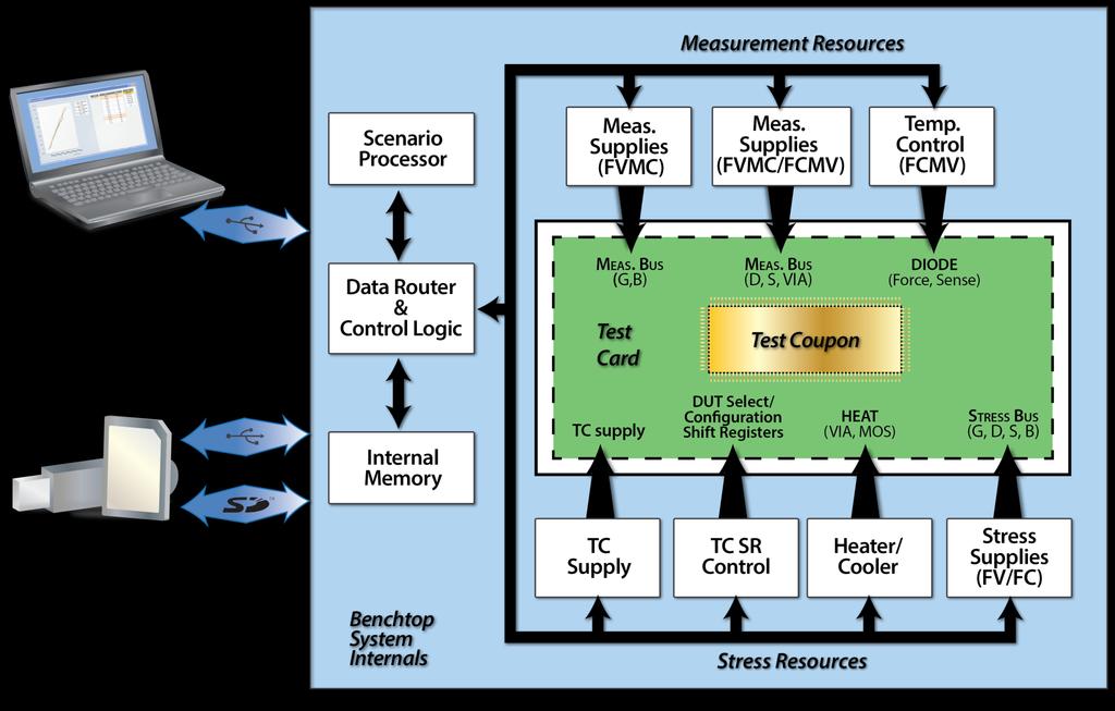

6 ProChek Architecture 6
7 ProChek Resource Overview ProChek offers full 4-terminal (gate, drain, source, body) control Resources: 4 Stress resources, serving to apply electrical stress can operate in Force Voltage (FV) or Force Current (FI) mode 4 SMUs, serving to collect data can operate in Force Voltage Measure Current (FVMI) or in Force Current (FI) mode, 10µs sampling, 4K data buffer per instrument, 24bit data Voltmeter Can operate in absolute or differential mode Can operate as slow (10µs sampling) or as fast (500ns sampling) meter Utilities Utility Voltage source Utility Current source Utility Voltmeter Heater/Cooler control 7
8 ProChek Extensions ProChek has provisions for expansion with additional (add-on) instruments. New ProChek Plus platform supports up to 24 (48) instruments/smus User specific test structures can easily be converted to a native ProChek test structure by means of an active interface board. 8
9 Analogy: Orchestra ProChek resources == musical instruments Scenario processor == Conductor Test Strategy == Music piece User == Composer ProChek Concept Controls how the music is played (key, timbre, ) Can write his own partitions Generic Test strategy support Can rely on predefined (but yet configurable) strategies (EM, SM, HCI, QBD, TDDB, xbti, ) 9
10 ProChek System ProChek Application Device under Test (DUT) or a set of DUTs Interface to link DUT with ProChek system Function of DUT nature (packaged, wafer structure, set of DUTs) Simple cable with appropriate connectors Passive Adapter/interface board with DUT socket Active interface board with DUT socket Probe card + link between probe card and ProChek system 10
11 Agenda Introduction ProChek & Test Structures ProChek WLR Application ProChek Test Considerations & Test Results ProChek Plus Summary Q&A. 11
12 ProChek & Test Structures 12
13 Agenda Introduction ProChek & Test Structures ProChek WLR Application ProChek Test Considerations & Test Results ProChek Plus Summary Q&A. 15

14 ProChek WLR Application 16

15 ProChek WLR Application 17

16 ProChek WLR Application Active Interface Board ProChek System Cable Interconnect to probe card 18
17 Agenda Introduction ProChek & Test Structures ProChek WLR Application ProChek Test Considerations & Test Results ProChek Plus Summary Q&A. 19


18 Technology (PDK) Verification ProChek s measured results closely matches test data provided by the foundry ProChek measures parameters, devices, and conditions NOT provided by the foundry Ids Vds measurements and simulations in the IBM BICMOS8HP process for different Vgs, from 0.3 to 1.5 V. 20
19 Device Characterization The ProChek approach allows for a statistical analysis of data relevant to quality monitoring. By increasing the volume of data recorded, a robust analysis can be performed. Ids Vds curves for 48 NFET DUTs Distribution of On Current in 48 NFET DUTs 21

20 Device Characterization ONC18 22
21 ProChek Capabilities ProChek can make voltage / current measurements at a 10µs interval (100KHz rate) Collecting up to 500 values per measurement point and per instrument All measurements are running concurrent ProChek s fast voltmeter can make voltage measurements at 500ns intervals (2MHz rate) Collecting up to 20K values per measurement point values can be linearly or logarithmically distributed over time Annealing function is designed to evaluate behaviors over time 23
22 ProChek Fast xbti Support FAST?! what do we mean? Ability to make measurements fast! Ability to quickly bring the DUT into a state of degradation so that it shows xbti effects! Ability to observe short lived degradation effects cancelled by annealing effects! Ability to make measurements very shortly after a DUT is switched from stress to measurement conditions before, during and after the transition from stress to measurement conditions 24
23 ProChek xbti support On-the-Fly Measurement Support 25
24 ProChek xbti support IDD only On-the-Fly Measurement Support 26
25 ProChek xbti support On-the-Fly Single Point Measurement Support 27

26 ProChek xbti support On-the-Fly Vth Measurement Support 28
27 Vth Degradation Results Measurement of Vds whilst maintaining Ids constant (IBM9SF 90nm techno) under voltage stress conditions 29
28 Vth Degradation Results 30
29 Agenda Introduction ProChek & Test Structures ProChek WLR Application ProChek Test Considerations & Test Results ProChek Plus Summary Q&A. 31

30 ProChek Plus 32

31 ProChek Plus 33
32 ProChek Plus Configurable Platform 4 slots serving Stress Resources or Low Resolution Measurement Instruments 8 slots serving High Resolution Measurement Resources Each slot can support up to 4 Resources Available Modules 4-channel configurable SMU module 2-channel configurable Voltmeter module Test Structure control module System control module 34
33 Agenda Introduction ProChek & Test Structures ProChek WLR Application ProChek Test Considerations & Test Results ProChek Plus Summary Q&A. 35


34 Summary ProChek Advanced, dedicated system for fabrication process characterization offering significant advantages to IC designers, process, and reliability engineers. Covers reliability concerns of modern nanotechnology processes, including radiation effects Covers qualification needs for new and immature processes Serving Wafer Level Tests without the need for additional equipment Significant cost and time savings 36

35 37
36 Slides and recording of the webinar will be available shortly via an from Ridgetop follow-up questions & comments to: Please fill out our brief feedback survey at Thanks for your time and interest! 38


37 Ridgetop Group, Inc West Ina Road Tucson, AZ
Ridgetop Group, Inc.
 Ridgetop Group, Inc. Ridgetop Group Facilities in Tucson, AZ Arizona-based firm, founded in 2000, with focus on electronics for critical applications Two divisions: Semiconductor & Precision Instruments
Semiconductor Process Reliability SVTW 2012 Esko Mikkola, Ph.D. & Andrew Levy
 Semiconductor Process Reliability SVTW 2012 Esko Mikkola, Ph.D. & Andrew Levy 1 IC Failure Modes Affecting Reliability Via/metallization failure mechanisms Electro migration Stress migration Transistor
Reliable Electronics? Precise Current Measurements May Tell You Otherwise. Hans Manhaeve. Ridgetop Europe
 Reliable Electronics? Precise Current Measurements May Tell You Otherwise Hans Manhaeve Overview Reliable Electronics Precise current measurements? Accurate - Accuracy Resolution Repeatability Understanding
Next Generation Curve Tracing & Measurement Tips for Power Device. Kim Jeong Tae RF/uW Application Engineer Keysight Technologies
 Next Generation Curve Tracing & Measurement Tips for Power Device Kim Jeong Tae RF/uW Application Engineer Keysight Technologies Agenda Page 2 Conventional Analog Curve Tracer & Measurement Challenges
WHITE PAPER CIRCUIT LEVEL AGING SIMULATIONS PREDICT THE LONG-TERM BEHAVIOR OF ICS
 WHITE PAPER CIRCUIT LEVEL AGING SIMULATIONS PREDICT THE LONG-TERM BEHAVIOR OF ICS HOW TO MINIMIZE DESIGN MARGINS WITH ACCURATE ADVANCED TRANSISTOR DEGRADATION MODELS Reliability is a major criterion for
EECS150 - Digital Design Lecture 19 CMOS Implementation Technologies. Recap and Outline
 EECS150 - Digital Design Lecture 19 CMOS Implementation Technologies Oct. 31, 2013 Prof. Ronald Fearing Electrical Engineering and Computer Sciences University of California, Berkeley (slides courtesy
DATE 2016 Early Reliability Modeling for Aging and Variability in Silicon System (ERMAVSS Workshop)
") March 2016 DATE 2016 Early Reliability Modeling for Aging and Variability in Silicon System (ERMAVSS Workshop) Ron Newhart Distinguished Engineer IBM Corporation March 19, 2016 1 2016 IBM Corporation Background
March 2016 DATE 2016 Early Reliability Modeling for Aging and Variability in Silicon System (ERMAVSS Workshop) Ron Newhart Distinguished Engineer IBM Corporation March 19, 2016 1 2016 IBM Corporation Background
Transient Current Measurement for Advance Materials & Devices
 & Devices 8 May 2017 Brian YEO Application Engineer Keysight Technologies Agenda 2 High speed data acquisition basics Challenges & solutions for transient current measurement. Considerations when making
What Is An SMU? SEP 2016
 What Is An SMU? SEP 2016 Agenda SMU Introduction Theory of Operation (Constant Current/Voltage Sourcing + Measure) Cabling : Triax vs Coax Advantages in Resistance Applications (vs. DMMs) Advantages in
Advanced PDK and Technologies accessible through ASCENT
 Advanced PDK and Technologies accessible through ASCENT MOS-AK Dresden, Sept. 3, 2018 L. Perniola*, O. Rozeau*, O. Faynot*, T. Poiroux*, P. Roseingrave^ olivier.faynot@cea.fr *Cea-Leti, Grenoble France;
SOURCE-MEASURE UNITS INCREASE PRODUCTIVITY AND ACCURACY IN AUTOMATED TESTING. Lee Stauffer. Keithley Instruments, Inc.
 SOURCE-MEASURE UNITS INCREASE PRODUCTIVITY AND ACCURACY IN AUTOMATED TESTING Lee Stauffer Keithley Instruments, Inc. Introduction Source-Measure Units (SMUs) are more than the next generation of power
Bias Stress Testing of SiC MOSFETs
 Bias Stress Testing of SiC MOSFETs Robert Shaw Manager, Test and Qualification August 15 th, 2014 Special thanks to the U.S. Department of Energy for funding this under SBIR DE-SC0011315. Outline Objectives
ENEE307 Lab 7 MOS Transistors 2: Small Signal Amplifiers and Digital Circuits
 ENEE307 Lab 7 MOS Transistors 2: Small Signal Amplifiers and Digital Circuits In this lab, we will be looking at ac signals with MOSFET circuits and digital electronics. The experiments will be performed
New Wide Band Gap High-Power Semiconductor Measurement Techniques Accelerate your emerging material device development
 New Wide Band Gap High-Power Semiconductor Measurement Techniques Accelerate your emerging material device development Alan Wadsworth Americas Market Development Manager Semiconductor Test Division July
Verification Structures for Transmission Line Pulse Measurements
 Verification Structures for Transmission Line Pulse Measurements R.A. Ashton Agere Systems, 9333 South John Young Parkway, Orlando, Florida, 32819 USA Phone: 44-371-731; Fax: 47-371-777; e-mail: rashton@agere.com
Keysight Technologies Improve the Accuracy and Efficiency for Organic-Thin Film Transistor (Organic-TFT) Characterization
 Characterization") Keysight Technologies Improve the Accuracy and Efficiency for Organic-Thin Film Transistor (Organic-TFT) Characterization B1500A Semiconductor Device Analyzer Application Note Introduction Organic materials
Keysight Technologies Improve the Accuracy and Efficiency for Organic-Thin Film Transistor (Organic-TFT) Characterization B1500A Semiconductor Device Analyzer Application Note Introduction Organic materials
I DDQ Current Testing
 I DDQ Current Testing Motivation Early 99 s Fabrication Line had 5 to defects per million (dpm) chips IBM wanted to get 3.4 defects per million (dpm) chips Conventional way to reduce defects: Increasing
Vector Network Analysis
 Portfolio Brochure Vector Network Analysis Product Portfolio Vector Network Analysis VNA Innovation Timeline In 1965, Anritsu filed the patent that defined the first modern Vector Network Analyzer (VNA).
Effect of Aging on Power Integrity of Digital Integrated Circuits
 Effect of Aging on Power Integrity of Digital Integrated Circuits A. Boyer, S. Ben Dhia Alexandre.boyer@laas.fr Sonia.bendhia@laas.fr 1 May 14 th, 2013 Introduction and context Long time operation Harsh
Introducing Pulsing into Reliability Tests for Advanced CMOS Technologies
 WHITE PAPER Introducing Pulsing into Reliability Tests for Advanced CMOS Technologies Pete Hulbert, Industry Consultant Yuegang Zhao, Lead Applications Engineer Keithley Instruments, Inc. AC, or pulsed,
A Unique System Concept to Improve the Accuracy of Wafer-Level Flicker-Noise Characterization. Andrej Rumiantsev, Stojan Kanev
 A Unique System Concept to Improve the Accuracy of Wafer-Level Flicker-Noise Characterization Andrej Rumiantsev, Stojan Kanev Content Motivation Challenges for 1/f Measurements New Probe System Concept
An Accelerated On-Wafer Test to Improve Long- Term Reliability of a 0.25 µm PHEMT Process
 An Accelerated On-Wafer Test to Improve Long- Term Reliability of a 0.25 µm PHEMT Process Wayne Struble, Jason Barrett, Nishant Yamujala MACOM January-4-17 September 28-30 2016, Pensacola Beach, Florida
Power. GaN. Rdyn in hard and soft-switching applications. P. Gassot, P. Moens, M. Tack, Corporate R&D Bodo Power Conference Munich, Dec.
 Power GaN Rdyn in hard and soft-switching applications P. Gassot, P. Moens, M. Tack, Corporate R&D Bodo Power Conference Munich, Dec. 2017 Acknowledgements The authors wish to acknowledge and thank the
Keysight Technologies Pulsed-IV Parametric Test Solutions. Selection Guide
 Keysight Technologies Pulsed-IV Parametric Test Solutions Selection Guide Introduction Pulsed-IV parametric testing is becoming an increasingly common requirement for the development of semiconductor process
IBIS in the Frequency Domain. Michael Mirmak Intel Corporation DAC IBIS Summit 2006 July 25, 2006
 IBIS in the Frequency Domain Michael Mirmak Intel Corporation DAC IBIS Summit 2006 July 25, 2006 Agenda Frequency Domain and Related Aspects Area 1: Maximum Switching Frequency Area 2: C_comp Stability
STM RH-ASIC capability
 STM RH-ASIC capability JAXA 24 th MicroElectronic Workshop 13 th 14 th October 2011 Prepared by STM Crolles and AeroSpace Unit Deep Sub Micron (DSM) is strategic for Europe Strategic importance of European
write-nanocircuits Direct-write Jaebum Joo and Joseph M. Jacobson Molecular Machines, Media Lab Massachusetts Institute of Technology, Cambridge, MA
 Fab-in in-a-box: Direct-write write-nanocircuits Jaebum Joo and Joseph M. Jacobson Massachusetts Institute of Technology, Cambridge, MA April 17, 2008 Avogadro Scale Computing / 1 Avogadro number s? Intel
Keysight Technologies B1500A Semiconductor Device Analyzer Ultra-Fast 1 μs NBTI Characterization Using the B1500A s WGFMU Module.
 Keysight Technologies B1500A Semiconductor Device Analyzer Ultra-Fast 1 μs NBTI Characterization Using the B1500A s WGFMU Module Application Note Introduction Reducing the time required to characterize
Keysight Technologies Pulsed-IV Parametric Test Solutions. Selection Guide
 Keysight Technologies Pulsed-IV Parametric Test Solutions Selection Guide Introduction Pulsed-IV parametric testing is becoming an increasingly common requirement for the development of semiconductor process
Precize voltage measurements of multichannel systems on transient temperature conditions
 INFOTEH-JAHORINA Vol. 16, March 2017. Precize voltage measurements of multichannel systems on transient temperature conditions Dejan Milošević, Miloš Radovanović Dialog Semiconductor Nabern, Germany dejan.milosevic@diasemi.com,
1KV PIV. High Voltage Pulsed IV measurements. Inovative Test System AMCAD ENGINEERING. June 2013
 1KV PIV Inovative Test System High Voltage Pulsed IV measurements AMCAD ENGINEERING June 2013 1 Agenda 1KV PIV Overview Pulsed IV measurement concept Main Specifications Integration with instruments Measurement
DATASHEET CADENCE QRC EXTRACTION
 DATASHEET Cadence QRC Etraction, the industry s premier 3D fullchip parasitic etractor that is independent of design style or flow, is a fast and accurate RLCK etraction solution used during design implementation
USCi MOSFET progress (ARL HVPT program)
") USCi MOSFET progress (ARL HVPT program) L. Fursin, X. Huang, W. Simon, M. Fox, J. Hostetler, X. Li, A. Bhalla Aug 18, 2016 Contents USCi product line 1200V MOSFET progress 10kV IGBT and MPS progress 2
USCi MOSFET progress (ARL HVPT program) L. Fursin, X. Huang, W. Simon, M. Fox, J. Hostetler, X. Li, A. Bhalla Aug 18, 2016 Contents USCi product line 1200V MOSFET progress 10kV IGBT and MPS progress 2
An Array-Based Circuit for Characterizing Latent Plasma-Induced Damage
 An Array-Based Circuit for Characterizing Latent Plasma-Induced Damage Won Ho Choi, Pulkit Jain and Chris H. Kim University of Minnesota, Minneapolis, MN choi0444@umn.edu www.umn.edu/~chriskim/ Purpose
An On-Chip NBTI Sensor for Measuring PMOS Threshold Voltage Degradation
 An On-Chip NBTI Sensor for Measuring PMOS Threshold Voltage Degradation John Keane Tae-Hyoung Kim Chris H. Kim Department of Electrical Engineering University of Minnesota, Minneapolis, MN {jkeane, thkim,
Digital Design and System Implementation. Overview of Physical Implementations
 Digital Design and System Implementation Overview of Physical Implementations CMOS devices CMOS transistor circuit functional behavior Basic logic gates Transmission gates Tri-state buffers Flip-flops
GATE & DRAIN Probe heads specifications
 GATE & DRAIN Probe heads specifications Page 1 /18 October 11, Ref 01102011 Table of contents 1 Main Characteristic of the Pulse IV System 3 1.1 General Description 3 1.2 Main features 4 1.3 Pulse Timing
Solving Connection Challenges in On-Wafer Power Semiconductor Device Test. Application Note Series. Introduction
 Number 3276 pplication Note Series Solving Connection Challenges in On-Wafer Power Semiconductor Device Test Introduction Measuring DC and capacitance parameters for high power semiconductor devices requires
Monolith Semiconductor Inc. ARL SiC MOSFET Workshop 14 August 2015
 Monolith Semiconductor Inc. ARL SiC MOSFET Workshop 14 August 2015 Kevin Matocha, President 408 Fannin Ave Round Rock, TX 78664 Bringing SiC to our World. Acknowledgments Office of Science SBIR Prog. Office
Ultra-Fast NBTI/PBTI Package for the Model 4200-SCS
 Best-in-class test speed allows faster, more complete device characterization Begin measuring BTI degradation as soon as 30ns after stress is removed Measure transistor V T in less than 1µs using I D V
4.1.2 InAs nanowire circuits fabricated by field-assisted selfassembly on a host substrate
 22 Annual Report 2010 - Solid-State Electronics Department 4.1.2 InAs nanowire circuits fabricated by field-assisted selfassembly on a host substrate Student Scientist in collaboration with R. Richter
EECS150 - Digital Design Lecture 15 - CMOS Implementation Technologies. Overview of Physical Implementations
 EECS150 - Digital Design Lecture 15 - CMOS Implementation Technologies Mar 12, 2013 John Wawrzynek Spring 2013 EECS150 - Lec15-CMOS Page 1 Overview of Physical Implementations Integrated Circuits (ICs)
EECS150 - Digital Design Lecture 9 - CMOS Implementation Technologies
 EECS150 - Digital Design Lecture 9 - CMOS Implementation Technologies Feb 14, 2012 John Wawrzynek Spring 2012 EECS150 - Lec09-CMOS Page 1 Overview of Physical Implementations Integrated Circuits (ICs)
Optimizing Automatic Parametric Test (APT) in Mixed Signal / Mems foundry
 in Mixed Signal / Mems foundry") Optimizing Automatic Parametric Test (APT) in Mixed Signal / Mems foundry Authors: Steffen Richter, Group Mgr PCM-Member Technical Staff, Xfab Silicon Foundries Alex Pronin, Ph.D, Lead Applications Engineer,
Optimizing Automatic Parametric Test (APT) in Mixed Signal / Mems foundry Authors: Steffen Richter, Group Mgr PCM-Member Technical Staff, Xfab Silicon Foundries Alex Pronin, Ph.D, Lead Applications Engineer,
A NEW DC MEASUREMENT PRINCIPLE TO FULLY COVER DEVICE SELF-HEATING
 -1- A NEW DC MEASUREMENT PRINCIPLE TO FULLY COVER DEVICE SELF-HEATING Keywords: Device Self-Heating During DC Measurement, Data Sampling After Self-Heating Reached Final Value, IC-CAP Demo File Contents:
Probing for oscilloscope
 Probing for oscilloscope Agenda - Notion de sonde en oscilloscopie - Structure des différentes sondes - Passives - Actives - Logiques - Différentielles - Comment choisir la bonne sonde - Nouvelle technologie
CD40174BMS. CMOS Hex D -Type Flip-Flop. Features. Pinout. Applications. Functional Diagram. Description. December 1992
 SEMICONDUCTOR CD17BMS December 199 CMOS Hex D -Type Flip-Flop Features Pinout High Voltage Type (V Rating) 5V, and 15V Parametric Ratings CD17BMS TOP VIEW Standardized, Symmetrical Output Characteristics
EE 320 L LABORATORY 9: MOSFET TRANSISTOR CHARACTERIZATIONS. by Ming Zhu UNIVERSITY OF NEVADA, LAS VEGAS 1. OBJECTIVE 2. COMPONENTS & EQUIPMENT
 EE 320 L ELECTRONICS I LABORATORY 9: MOSFET TRANSISTOR CHARACTERIZATIONS by Ming Zhu DEPARTMENT OF ELECTRICAL AND COMPUTER ENGINEERING UNIVERSITY OF NEVADA, LAS VEGAS 1. OBJECTIVE Get familiar with MOSFETs,
Prerelease product(s)
") Datasheet Aerospace 60 A - 200 V fast recovery rectifier STTH60200CSA1 31218 FR SMD1 Features Very small conduction losses Negligible switching losses High surge current capability Hermetic package TID
Datasheet Aerospace 60 A - 200 V fast recovery rectifier STTH60200CSA1 31218 FR SMD1 Features Very small conduction losses Negligible switching losses High surge current capability Hermetic package TID
ANITA ROSS Trigger/Digitizer/DAQ. Gary S. Varner University of Hawai, i, Manoa ANITA Collaboration JPL March 2004
 ANITA ROSS Trigger/Digitizer/DAQ Gary S. Varner University of Hawai, i, Manoa ANITA Collaboration Meeting @ JPL March 2004 Overview System overview Reiterate, with ROSS simplifications ROSS trigger descope
Emulation of junction field-effect transistors for real-time audio applications
 This article has been accepted and published on J-STAGE in advance of copyediting. Content is final as presented. IEICE Electronics Express, Vol.* No.*,*-* Emulation of junction field-effect transistors
EE 230 Lab Lab 9. Prior to Lab
 MOS transistor characteristics This week we look at some MOS transistor characteristics and circuits. Most of the measurements will be done with our usual lab equipment, but we will also use the parameter
Low noise Amplifier, simulated and measured.
 Low noise Amplifier, simulated and measured. Introduction: As a study project a low noise amplifier shaper for capacitive detectors in AMS 0.6 µm technology is designed and realised. The goal was to design
Manufacturing Case Studies: Copy Exactly (CE!) and the two-year cycle at Intel
 and the two-year cycle at Intel") Manufacturing Case Studies: Copy Exactly (CE!) and the two-year cycle at Intel Paolo A. Gargini Director Technology Strategy Intel Fellow 1 Agenda 2-year cycle Copy Exactly Conclusions 2 I see no reason
Manufacturing Case Studies: Copy Exactly (CE!) and the two-year cycle at Intel Paolo A. Gargini Director Technology Strategy Intel Fellow 1 Agenda 2-year cycle Copy Exactly Conclusions 2 I see no reason
Impact of Basal Plane Dislocations and Ruggedness of 10 kv 4H-SiC Transistors
 11th International MOS-AK Workshop (co-located with the IEDM and CMC Meetings) Silicon Valley, December 5, 2018 Impact of Basal Plane Dislocations and Ruggedness of 10 kv 4H-SiC Transistors *, A. Kumar,
CharFlo-Cell! Cell! Next-Generation Solution for Characterizing and Modeling Standard Cell and I/O Library
 CharFlo-Cell! Cell! TM Next-Generation Solution for Characterizing and Modeling Standard Cell and I/O Library Agenda Introduction The Flow of CharFlo-Cell! The Applications and Features BiSection Methods
DARPA TRUST in IC s Effort. Dr. Dean Collins Deputy Director, MTO 7 March 2007
 DARPA TRUST in IC s Effort Dr. Dean Collins Deputy Director, MTO 7 March 27 Report Documentation Page Form Approved OMB No. 74-88 Public reporting burden for the collection of information is estimated
Sophisticated Power Loss Analysis Using A Digital Phosphor Oscilloscope
 Sophisticated Power Loss Analysis Using A Digital Phosphor Oscilloscope Quickly Locate Power Dissipation in Switching Power Supplies With demand for power driving architectural changes to switching power
2520 Pulsed Laser Diode Test System
 Complete pulse test of laser diode bars and chips with dual photocurrent measurement channels 0 Pulsed Laser Diode Test System Simplifies laser diode L-I-V testing prior to packaging or active temperature
A Perspective on Semiconductor Equipment. R. B. Herring March 4, 2004
 A Perspective on Semiconductor Equipment R. B. Herring March 4, 2004 Outline Semiconductor Industry Overview of circuit fabrication Semiconductor Equipment Industry Some equipment business strategies Product
Depletion-mode operation ( 공핍형 ): Using an input gate voltage to effectively decrease the channel size of an FET
: Using an input gate voltage to effectively decrease the channel size of an FET") Ch. 13 MOSFET Metal-Oxide-Semiconductor Field-Effect Transistor : I D D-mode E-mode V g The gate oxide is made of dielectric SiO 2 with e = 3.9 Depletion-mode operation ( 공핍형 ): Using an input gate voltage
Ch. 13 MOSFET Metal-Oxide-Semiconductor Field-Effect Transistor : I D D-mode E-mode V g The gate oxide is made of dielectric SiO 2 with e = 3.9 Depletion-mode operation ( 공핍형 ): Using an input gate voltage
Impact of Interconnect Length on. Degradation
 Impact of Interconnect Length on BTI and HCI Induced Frequency Degradation Xiaofei Wang, Pulkit Jain, Dong Jiao and Chris H. Kim University of Minnesota, Minneapolis, MN xfwang@umn.edu www.umn.edu/~chriskim/
Welcome! Device Characterization with the Keithley Model 4200-SCS Characterization System.
 Welcome! Device Characterization with the Keithley Model 4200-SCS Characterization System Safety Precautions Working with Electricity Before starting, check cables for cracks or wear. Get new cables if
Automated Semiconductor Device Measurement System for Temperature and Magnetic Field Characterization
 Session 2259 Automated Semiconductor Device Measurement System for Temperature and Magnetic Field Characterization M.G. Guvench, M. Rollins, S. Guvench and M. Denton University of Southern Maine Summary
Low Power Design of Successive Approximation Registers
 Low Power Design of Successive Approximation Registers Rabeeh Majidi ECE Department, Worcester Polytechnic Institute, Worcester MA USA rabeehm@ece.wpi.edu Abstract: This paper presents low power design
HINP4 Progress Report
 HINP4 Progress Report George Engel, D.Sc. Srikanth Thota (student) IC Design Research Laboratory Department of Electrical and Computer Engineering Southern Illinois University Edwardsville, IL, 62026-1801
High Speed Digital Systems Require Advanced Probing Techniques for Logic Analyzer Debug
 JEDEX 2003 Memory Futures (Track 2) High Speed Digital Systems Require Advanced Probing Techniques for Logic Analyzer Debug Brock J. LaMeres Agilent Technologies Abstract Digital systems are turning out
Front-To-Back MMIC Design Flow with ADS. Speed MMICs to market Save money and achieve high yield
 Front-To-Back MMIC Design Flow with ADS Speed MMICs to market Save money and achieve high yield 1 Unique Tools for Robust Designs, First Pass, and High Yield Yield Sensitivity Histogram (YSH) to components
Lecture Integrated circuits era
 Lecture 1 1.1 Integrated circuits era Transistor was first invented by William.B.Shockley, Walter Brattain and John Bardeen of Bell laboratories. In 1961, first IC was introduced. Levels of Integration:-
of High Power Semiconductor Device Testing
 Tips, Tricks, and Traps of High Power Semiconductor Device Testing 张卫华 KEITHLEY INSTRUMENTS 1 8/20/2012 2012 Keithley Instruments, Inc. 2012 Keithley Instruments, Inc. Overview The goal of this seminar
FDTD SPICE Analysis of High-Speed Cells in Silicon Integrated Circuits
 FDTD Analysis of High-Speed Cells in Silicon Integrated Circuits Neven Orhanovic and Norio Matsui Applied Simulation Technology Gateway Place, Suite 8 San Jose, CA 9 {neven, matsui}@apsimtech.com Abstract
2.5D Platform (Examples of products produced to date are shown here to demonstrate Amkor's production capabilities)
") Wafer Finishing & Flip Chip Stacking interconnects have emerged to serve a wide range of 2.5D- & 3D- packaging applications and architectures that demand very high performance and functionality at the
Wafer Finishing & Flip Chip Stacking interconnects have emerged to serve a wide range of 2.5D- & 3D- packaging applications and architectures that demand very high performance and functionality at the
Keysight Technologies Accurate NBTI Characterization Using Timing-on-the-fly Sampling Mode. Application Note
 Keysight Technologies Accurate NBTI Characterization Using Timing-on-the-fly Sampling Mode Application Note Introduction Keysight B1500A Semiconductor Device Analyzer Controlled dynamic recovery with 100
Probing Techniques for Signal Performance Measurements in High Data Rate Testing
 Probing Techniques for Signal Performance Measurements in High Data Rate Testing K. Helmreich, A. Lechner Advantest Test Engineering Solutions GmbH Contents: 1 Introduction: High Data Rate Testing 2 Signal
Precision INSTRUMENTATION AMPLIFIER
 Precision INSTRUMENTATION AMPLIFIER FEATURES LOW OFFSET VOLTAGE: µv max LOW DRIFT:.µV/ C max LOW INPUT BIAS CURRENT: na max HIGH COMMON-MODE REJECTION: db min INPUT OVER-VOLTAGE PROTECTION: ±V WIDE SUPPLY
Non-Volatile Memory Characterization and Measurement Techniques
 Non-Volatile Memory Characterization and Measurement Techniques Alex Pronin Keithley Instruments, Inc. 1 2012-5-21 Why do more characterization? NVM: Floating gate Flash memory Very successful; lead to
Automotive TFQ. A brief introduction of automotive test for quality Jonathan Ying
 Automotive TFQ A brief introduction of automotive test for quality Jonathan Ying 1 Why do we need this? Its quite simple quality in automotive safety applications is critical,automotive OEM require 0 DPPM
CMOS 120 GHz Phase-Locked Loops Based on Two Different VCO Topologies
 JOURNAL OF ELECTROMAGNETIC ENGINEERING AND SCIENCE, VOL. 17, NO. 2, 98~104, APR. 2017 http://dx.doi.org/10.5515/jkiees.2017.17.2.98 ISSN 2234-8395 (Online) ISSN 2234-8409 (Print) CMOS 120 GHz Phase-Locked
Curve Tracer Laboratory Assistant Using the Analog Discovery Module as A Curve Tracer
 Curve Tracer Laboratory Assistant Using the Analog Discovery Module as A Curve Tracer The objective of this lab is to become familiar with methods to measure the dc current-voltage (IV) behavior of diodes
New Generation Reliability Model
 New Generation Reliability Model S.-Y. Liao, C. Huang, T. Guo, A. Chen, Jushan Xie, Cadence Design Systems, Inc. S. Guo, R. Wang, Z. Yu, P. Hao, P. Ren, Y. Wang, R. Huang, Peking University Dec. 5th, 2016
TPH3207WS TPH3207WS. GaN Power Low-loss Switch PRODUCT SUMMARY (TYPICAL) Absolute Maximum Ratings (T C =25 C unless otherwise stated)
 Absolute Maximum Ratings (T C =25 C unless otherwise stated)") PRODUCT SUMMARY (TYPICAL) V DS (V) 650 R DS(on) (m ) 35 Q rr (nc) 175 Features Low Q rr Free-wheeling diode not required Quiet Tab for reduced EMI at high dv/dt GSD pin layout improves high speed design
PRODUCT SUMMARY (TYPICAL) V DS (V) 650 R DS(on) (m ) 35 Q rr (nc) 175 Features Low Q rr Free-wheeling diode not required Quiet Tab for reduced EMI at high dv/dt GSD pin layout improves high speed design
UNIT-III POWER ESTIMATION AND ANALYSIS
 UNIT-III POWER ESTIMATION AND ANALYSIS In VLSI design implementation simulation software operating at various levels of design abstraction. In general simulation at a lower-level design abstraction offers
Technology Transfers Opportunities, Process and Risk Mitigation. Radhika Srinivasan, Ph.D. IBM
 Technology Transfers Opportunities, Process and Risk Mitigation Radhika Srinivasan, Ph.D. IBM Abstract Technology Transfer is quintessential to any technology installation or semiconductor fab bring up.
Application Overview: Simplified I/V Characterization of DC-DC Converters
 Application Overview: Simplified I/V Characterization of DC-DC Converters What is a SMU? Source measure units (SMUs) are an all-in-one solution for current voltage (I/V) characterization with the combined
FACULTY OF ENGINEERING LAB SHEET ENT 3036 SEMICONDUCTOR DEVICES TRIMESTER
 FACULTY OF ENGINEERING LAB SHEET ENT 3036 SEMICONDUCTOR DEVICES TRIMESTER 3 2017-2018 SD1 I-V MEASUREMENT OF MOS CAPACITOR *Note: On-the-spot evaluation may be carried out during or at the end of the experiment.
Lecture 6: Electronics Beyond the Logic Switches Xufeng Kou School of Information Science and Technology ShanghaiTech University
 Lecture 6: Electronics Beyond the Logic Switches Xufeng Kou School of Information Science and Technology ShanghaiTech University EE 224 Solid State Electronics II Lecture 3: Lattice and symmetry 1 Outline
Current sensor by IZM
 Current sensor by IZM TYPICAL APPLICATIONS Current measurement in commutation cell Monitoring of switching behavior of Si, SiC, GaN, or similar semiconductors Measuring of current pulses Analysis of power
AC Current Probes CT1 CT2 CT6 Data Sheet
 View at www.testequipmentdepot.com AC Current Probes CT1 CT2 CT6 Data Sheet Features & Benefits High Bandwidth Ultra-low Inductance Very Small Form Factor Characterize Current Waveforms up to
Testing Digital Systems II
 Lecture : Introduction Instructor: M. Tahoori Copyright 206, M. Tahoori TDS II: Lecture Today s Lecture Logistics Course Outline Review from TDS I Copyright 206, M. Tahoori TDS II: Lecture 2 Lecture Logistics
Optimization of Wafer Level Test Hardware using Signal Integrity Simulation
 June 7-10, 2009 San Diego, CA Optimization of Wafer Level Test Hardware using Signal Integrity Simulation Jason Mroczkowski Ryan Satrom Agenda Industry Drivers Wafer Scale Test Interface Simulation Simulation
Digital Step Attenuator
 Wide band Digital Step Attenuator 50Ω 0 to 31.75, 0.25 Step 9 khz to 6.0 GHz 7 Bit, Parallel control interface, Single Supply Voltage The Big Deal Wideband, operates up to 6 GHz Immune to latchup High
Measurement and Analysis for Switchmode Power Design
 Measurement and Analysis for Switchmode Power Design Switched Mode Power Supply Measurements AC Input Power measurements Safe operating area Harmonics and compliance Efficiency Switching Transistor Losses
Computer Controlled Curve Tracer
 Computer Controlled Curve Tracer Christopher Curro The Cooper Union New York, NY Email: chris@curro.cc David Katz The Cooper Union New York, NY Email: katz3@cooper.edu Abstract A computer controlled curve
Revision: Jan 29, E Main Suite D Pullman, WA (509) Voice and Fax
 Voice and Fax") Revision: Jan 29, 2011 215 E Main Suite D Pullman, WA 99163 (509) 334 6306 Voice and Fax Overview The purpose of this lab assignment is to provide users with an introduction to some of the equipment which
Revision: Jan 29, 2011 215 E Main Suite D Pullman, WA 99163 (509) 334 6306 Voice and Fax Overview The purpose of this lab assignment is to provide users with an introduction to some of the equipment which
Introduction to VLSI ASIC Design and Technology
 Introduction to VLSI ASIC Design and Technology Paulo Moreira CERN - Geneva, Switzerland Paulo Moreira Introduction 1 Outline Introduction Is there a limit? Transistors CMOS building blocks Parasitics
PHYTER 100 Base-TX Reference Clock Jitter Tolerance
 PHYTER 100 Base-TX Reference Clock Jitter Tolerance 1.0 Introduction The use of a reference clock that is less stable than those directly driven from an oscillator may be required for some applications.
nanomca 80 MHz HIGH PERFORMANCE, LOW POWER DIGITAL MCA Model Numbers: NM0530 and NM0530Z
 datasheet nanomca 80 MHz HIGH PERFORMANCE, LOW POWER DIGITAL MCA Model Numbers: NM0530 and NM0530Z I. FEATURES Finger-sized, high performance digital MCA. 16k channels utilizing smart spectrum-size technology
Gallium nitride (GaN)
") 80 Technology focus: GaN power electronics Vertical, CMOS and dual-gate approaches to gallium nitride power electronics US research company HRL Laboratories has published a number of papers concerning
80 Technology focus: GaN power electronics Vertical, CMOS and dual-gate approaches to gallium nitride power electronics US research company HRL Laboratories has published a number of papers concerning
Semiconductor Materials for Power Electronics (SEMPEL) GaN power electronics materials
 GaN power electronics materials") Semiconductor Materials for Power Electronics (SEMPEL) GaN power electronics materials Kjeld Pedersen Department of Physics and Nanotechnology, AAU SEMPEL Semiconductor Materials for Power Electronics
Semiconductor Materials for Power Electronics (SEMPEL) GaN power electronics materials Kjeld Pedersen Department of Physics and Nanotechnology, AAU SEMPEL Semiconductor Materials for Power Electronics
Ultra640 SCSI with Receiver Equalization, 25 meters into a Backplane with 6 loads. Russ Brown Quantum Corporation
 T1/-154r Ultra64 SCSI with Receiver Equalization, 25 meters into a Backplane with 6 loads Russ Brown Quantum Corporation SCSI Physical Working Group Meeting 7 March 2 Dallas, TX U64 25 Meter Cable Test