ANITA ROSS Trigger/Digitizer/DAQ. Gary S. Varner University of Hawai, i, Manoa ANITA Collaboration JPL March 2004
|
|
|
- Sabina Cox
- 6 years ago
- Views:
Transcription

1 ANITA ROSS Trigger/Digitizer/DAQ Gary S. Varner University of Hawai, i, Manoa ANITA Collaboration JPL March 2004
2 Overview System overview Reiterate, with ROSS simplifications ROSS trigger descope System descope Buffer depth Sampling record Critical R&D Items Largely the same STRAW3 LABRADOR as is More detail on LABRADOR 1
3 Proposed Signal Flow Trigger LNA Gain [GHz] Digitize [GHz] 2
4 Updated August 03 Baseline ANITA Sampling Unit for RF (SURF) Board 3
5 ROSS Single-Crate Scheme During Aug 2003 Collab Meeting challenged to go to 4 Antenna/Digitizer Card Transition module TURF boards CPU Crate Top View PCI bus 1 PCI bus 2 7 drops max 40 channel scenario 4 antenna SURF boards 4 spare cpci slots for other functionality (GPS, housekeeping?) 4


6 STRAW3 Data Sheet Available on the ID Lab web-site A number of SPICE Simulations of Performance Expectations 5

7 STRAW Architecture 0.25µm TSMC process 6
8 Self-Triggering 7
9 Digital-to-Analog Convert Fine-adjust DAC Main DAC DAC Code 8


10 Fine Adjust R 2R 9
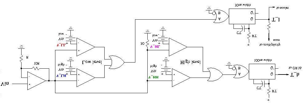
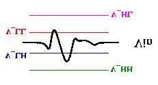
11 Triggering Detail 10

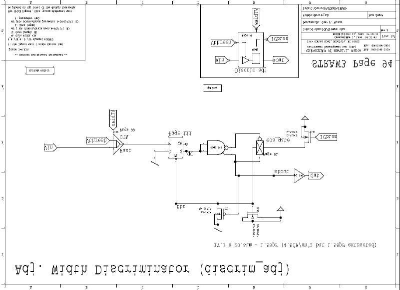
12 Discriminator Layout Fast Comparator Control Logic Capacitor 11

13 Simulation Results Use simulated high freq. Response from beamtest data: works 12


14 RFCeval 0 th order prototype Quick Reference: RFCeval == Radio Freq Comp evaluation board STRAW == Self-Triggered Recorder for Analog Waveforms LABRADOR == Large Analog Bandwidth Recorder And Digitizer with Ordered Readout 13


15 TURFpro project Prototyping: On-board amps Limited Multi-banding RF power monitoring Local trigger processor Sr. EE Project Develop Feedback Control Loop By defn will be Done by end of Semester DACs DACs 32-b scaler 32-b scaler Other Projects Considering 2-chip soln: Super-RICE SKAM 14
16 Updated August 03 Baseline ANITA Sampling Unit for RF (SURF) Board 15
17 LABRADOR Goals Maximum input bandwidth 50Ω impedance Simplified architecture (no trigger functionality) best RF coupling into Switched Capacitor storage cells Classical engineering trade-offs Input trace resistance vs. load capacitance Storage capacitor ktc noise vs. load capacitance Storage switch R on vs. drain load capacitance Analog Transfer Optimum speed Individual channel parallel Improved ADC Ramp type no missing codes Massively parallel to reduce conversion time Today s part See SMEX Talk 16

18 LABRADOR Architecture 0.25µm TSMC process 17


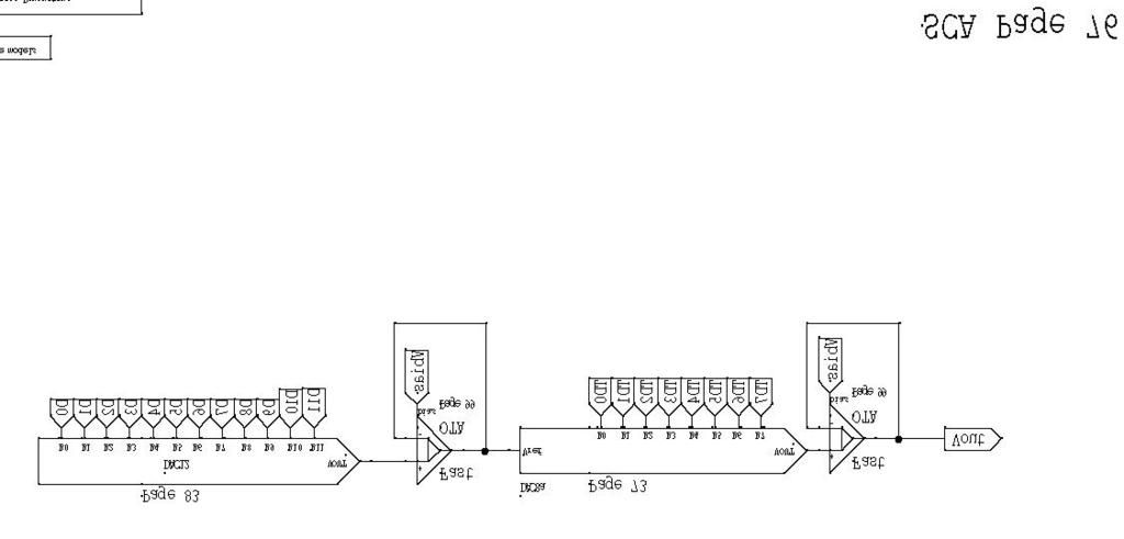
19 LABRADOR floorplan Straight Shot RF inputs 128x Wilk ADCs Analog Superbuffers 8 chan. * 256 samples 8x HS Analog out, 1x MUX out Random access: 18


20 STRAW ADC Expectations worst case for mismatch in a previous implementation of same SAR ADC w/r-2r ladder Can correct to rather linear, but still differential sensitivity and calibration is a pain Wilkinson type better monotonic BUT, slower 19

21 Wilkinson ADC No missing codes Linearity as good as can make ramp Can bracket range of interest + - NB: SCA output not linear 20
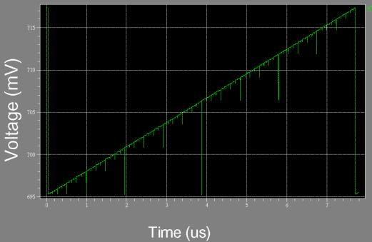
22 ADC Sim Wilkinson ADC SPICE Sim Output code [counts] y = x R 2 = Wilk ADC Linear (Wilk ADC) Input Voltage [V] 21
 [mv] 700 600 500 400 300 200 100 Gain: Rload = 40k y = 6.2891x - 2364.")
23 Transfer Curve Storage Cell Simulation v kt C rms = = 0. 5 store mv Diff sensed Voltage (Vout) [mv] Gain: Rload = 40k y = x R 2 = Stored Waveform (Vin) [mv] 22
24 Readout speed comparison IC STRAW2 - GEISER STRAW2 DALI ADC EXT EXT speed 8MHz 1MHz Total Latency 384 µs 3,072 µs Evt. Size 6kB STRAW3 -- SURF STRAW3 -- FINESSE INT EXT 2.5MHz 10MHz (a) 1,638 µs 410 µs 8kB LABRADOR -- SURF INT 100kHz (b) 240 µs LABRADOR -- serial EXT 10MHz 210 µs 4kB LABRADOR -- parallel EXT 20MHz 12.8 µs (a) 16 channels for STRAW3, 12 channels for STRAW2 (b) 12.8MHz effective: 128x ADC; 100MHz clock, 12b eff. includes additional latency 8x 20MHz ADC in parallel (>300MB/s!!) 23
25 Aside: LABRADOR sampling speed High/Low CTRL: Extend to 4 GSa/s Improve odd/event Low freq operation Sampling Freq. [GHz] STRAW2 Sampling Freq. Avg. -cycle +cycle SPICE Freq. Adj. Voltage (ROVDD) [V] 24
26 ROSS Delineations Greatly simplified Global Trigger Most logic done locally > 1 bit/surf? L1 trigger only VETO? 2x Buffer depth Compromises on the trigger banding? Reduced RF monitoring No active RF pulser circuit Depend upon Noise Diode Any problem with this? 25
 RFCeval Testing Summary Plans: RFCeval board in debug STRAW3 chip alive LABRADOR returns ~ now (also test on RFCeval) Plan to leverage interest of other groups on testing")
27 Summary R&D into critical (non-standard) components: Good progress on meeting specs Pending write-ups (works in progress): LABRADOR Data Sheet ( RFCeval Testing Summary Plans: RFCeval board in debug STRAW3 chip alive LABRADOR returns ~ now (also test on RFCeval) Plan to leverage interest of other groups on testing Design conflict: SMEX vs. ROSS 26
28 Back-up slides 27
 Significant signal")

29 Askaryan Signature Time (ns) Significant signal power at large frequencies Strong linear polarization (near 100%) 28
ANITA SMEX Digitizer/DAQ. Gary S. Varner University of Hawai, i, Manoa ANITA Collaboration JPL March 2004
 ANITA SMEX Digitizer/DAQ Gary S. Varner University of Hawai, i, Manoa ANITA Collaboration Meeting @ JPL March 2004 Overview System overview SMEX Trigger items covered by Andre ROSS descope in Part II Summary
SalSA Readout: GEISER & Digitizers. Gary S. Varner Univ. of Hawaii February 2005
 SalSA Readout: GEISER & Digitizers Gary S. Varner Univ. of Hawaii February 2005 Outline Transient Recording Have explored 3 techniques through prototype measurement stage For more than a year have been
Large Analog Bandwidth Recorder and Digitizer with Ordered Readout (Perf, Results)
") Large Analog Bandwidth Recorder and Digitizer with Ordered Readout (Perf, Results) Gary S. Varner University of Hawai i U Chicago Precision Timing Mtg Dec.07 Topics Background to WFS Development Antarctic
Large Analog Bandwidth Recorder and Digitizer with Ordered Readout (Perf, Results) Gary S. Varner University of Hawai i U Chicago Precision Timing Mtg Dec.07 Topics Background to WFS Development Antarctic
A 4 Channel Waveform Sampling ASIC in 130 nm CMOS
 A 4 Channel Waveform Sampling ASIC in 130 nm CMOS E. Oberla, H. Grabas, J.F. Genat, H. Frisch Enrico Fermi Institute, University of Chicago K. Nishimura, G. Varner University of Hawai I Large Area Picosecond
A 4-Channel Fast Waveform Sampling ASIC in 130 nm CMOS
 A 4-Channel Fast Waveform Sampling ASIC in 130 nm CMOS E. Oberla, H. Grabas, M. Bogdan, J.F. Genat, H. Frisch Enrico Fermi Institute, University of Chicago K. Nishimura, G. Varner University of Hawai I
SURF n TURF. Gary S. Varner University of Hawai, i, Manoa ANITA Collaboration UC Irvine April 7 th, 2005
 SURF n TURF Gary S. Varner University of Hawai, i, Manoa ANITA Collaboration Meeting @ UC Irvine April 7 th, 25 Talks Overview: 2 parts Sampling Unit for RF (SURF) evolution Digitization: STRAW, LABRADOR
Station Overview, ARA Trigger & Digitizer
 Station Overview, ARA Trigger & Digitizer Station geometry Triggering Overview Trigger Simulation Geometrical constraints Trigger rates Digitization & Data rates Gary S. Varner ARA Workshop in Honolulu,
Development of a 20 GS/s Sampling Chip in 130nm CMOS Technology
 Development of a 20 GS/s Sampling Chip in 130nm CMOS Technology 2009 IEEE Nuclear Science Symposium, Orlando, Florida, October 28 th 2009 Jean-Francois Genat On behalf of Mircea Bogdan 1, Henry J. Frisch
Ice Radio Sampler (IRS) & Buffered LABRADOR #3 (BLAB3) Preliminary Specification Review. Gary S. Varner Internal ID Lab Review, 10 AUG 09
 & Buffered LABRADOR #3 (BLAB3) Preliminary Specification Review. Gary S. Varner Internal ID Lab Review, 10 AUG 09") Ice Radio Sampler (IRS) & Buffered LABRADOR #3 (BLAB3) Preliminary Specification Review Gary S. Varner Internal ID Lab Review, 10 AUG 09 Goals for both ASICs Confirm Design Specifications Table Listing
Ice Radio Sampler (IRS) & Buffered LABRADOR #3 (BLAB3) Preliminary Specification Review Gary S. Varner Internal ID Lab Review, 10 AUG 09 Goals for both ASICs Confirm Design Specifications Table Listing
SalSA Readout: An update on architectures. Gary S. Varner Univ. of Hawaii May 2005
 SalSA Readout: An update on architectures Gary S. Varner Univ. of Hawaii May 2005 Update since Feb. Mtg @ SLAC Considering 4 schemes: In hole (D RITOS based): GEISER type 100bT type, trigger packets sent
Buffered LABRADOR (BLAB3) Design Review. Gary S. Varner 4 NOV 09
 Design Review. Gary S. Varner 4 NOV 09") Buffered LABRADOR (BLAB3) Design Review Gary S. Varner 4 NOV 09 Baseline confirmation Goals for today Ice Radio Sampler (IRS) as sampling/storage array basis High rate/long latency architecture Review
Buffered LABRADOR (BLAB3) Design Review Gary S. Varner 4 NOV 09 Baseline confirmation Goals for today Ice Radio Sampler (IRS) as sampling/storage array basis High rate/long latency architecture Review
A 4 GSample/s 8-bit ADC in. Ken Poulton, Robert Neff, Art Muto, Wei Liu, Andrew Burstein*, Mehrdad Heshami* Agilent Laboratories Palo Alto, California
 A 4 GSample/s 8-bit ADC in 0.35 µm CMOS Ken Poulton, Robert Neff, Art Muto, Wei Liu, Andrew Burstein*, Mehrdad Heshami* Agilent Laboratories Palo Alto, California 1 Outline Background Chip Architecture
ANITA-Lite Trigger Object (ALTO Rev. B) User s Manual
 User s Manual") ANITA-Lite Trigger Object (ALTO Rev. B) User s Manual Gary S. Varner, David Ridley, James Kennedy and Mary Felix Contact: varner@phys.hawaii.edu Instrumentation Development Laboratory Department of Physics
ANITA-Lite Trigger Object (ALTO Rev. B) User s Manual Gary S. Varner, David Ridley, James Kennedy and Mary Felix Contact: varner@phys.hawaii.edu Instrumentation Development Laboratory Department of Physics
Belle Monolithic Thin Pixel Upgrade -- Update
 Belle Monolithic Thin Pixel Upgrade -- Update Gary S. Varner On Behalf of the Pixel Gang (Marlon, Fang, ) Local Belle Meeting March 2004 Univ. of Hawaii Today s delta Have shown basic scheme before Testing
Digital PWM IC Control Technology and Issues
 Digital PWM IC Control Technology and Issues Prof. Seth R. Sanders Angel V. Peterchev Jinwen Xiao Jianhui Zhang Department of EECS University of California, Berkeley Digital Control Advantages implement
8-Bit A/D Converter AD673 REV. A FUNCTIONAL BLOCK DIAGRAM
 a FEATURES Complete 8-Bit A/D Converter with Reference, Clock and Comparator 30 s Maximum Conversion Time Full 8- or 16-Bit Microprocessor Bus Interface Unipolar and Bipolar Inputs No Missing Codes Over
PART TOP VIEW V EE 1 V CC 1 CONTROL LOGIC
 19-1331; Rev 1; 6/98 EVALUATION KIT AVAILABLE Upstream CATV Driver Amplifier General Description The MAX3532 is a programmable power amplifier for use in upstream cable applications. The device outputs
Quad 12-Bit Digital-to-Analog Converter (Serial Interface)
") Quad 1-Bit Digital-to-Analog Converter (Serial Interface) FEATURES COMPLETE QUAD DAC INCLUDES INTERNAL REFERENCES AND OUTPUT AMPLIFIERS GUARANTEED SPECIFICATIONS OVER TEMPERATURE GUARANTEED MONOTONIC OVER
Quad 1-Bit Digital-to-Analog Converter (Serial Interface) FEATURES COMPLETE QUAD DAC INCLUDES INTERNAL REFERENCES AND OUTPUT AMPLIFIERS GUARANTEED SPECIFICATIONS OVER TEMPERATURE GUARANTEED MONOTONIC OVER
Test Results of the HTADC12 12 Bit Analog to Digital Converter at 250 O C
 Test Results of the HTADC12 12 Bit Analog to Digital Converter at 250 O C Thomas J. Romanko and Mark R. Larson Honeywell International Inc. Honeywell Aerospace, Defense & Space 12001 State Highway 55,
Towards an ADC for the Liquid Argon Electronics Upgrade
 1 Towards an ADC for the Liquid Argon Electronics Upgrade Gustaaf Brooijmans Upgrade Workshop, November 10, 2009 2 Current LAr FEB Existing FEB (radiation tolerant for LHC, but slhc?) Limits L1 latency
M8190A 12 GSa/s Arbitrary Waveform Generator
 M8190A 12 GSa/s Arbitrary Waveform Generator March 1 st Question and Answer session 1. How much are the instruments? The starting price is $78,000 containing o 1 channel option with $55,000 o 14 bit option
A radiation tolerant, low-power cryogenic capable CCD readout system:
 A radiation tolerant, low-power cryogenic capable CCD readout system: Enabling focal-plane mounted CCD read-out for ground or space applications with a pair of ASICs. Overview What do we want to read out
LM12L Bit + Sign Data Acquisition System with Self-Calibration
 LM12L458 12-Bit + Sign Data Acquisition System with Self-Calibration General Description The LM12L458 is a highly integrated 3.3V Data Acquisition System. It combines a fully-differential self-calibrating
Low Cost 10-Bit Monolithic D/A Converter AD561
 a FEATURES Complete Current Output Converter High Stability Buried Zener Reference Laser Trimmed to High Accuracy (1/4 LSB Max Error, AD561K, T) Trimmed Output Application Resistors for 0 V to +10 V, 5
ADC Bit High-Speed µp-compatible A/D Converter with Track/Hold Function
 10-Bit High-Speed µp-compatible A/D Converter with Track/Hold Function General Description Using a modified half-flash conversion technique, the 10-bit ADC1061 CMOS analog-to-digital converter offers very
8-Bit, high-speed, µp-compatible A/D converter with track/hold function ADC0820
 8-Bit, high-speed, µp-compatible A/D converter with DESCRIPTION By using a half-flash conversion technique, the 8-bit CMOS A/D offers a 1.5µs conversion time while dissipating a maximum 75mW of power.
INTEGRATED CIRCUITS. AN109 Microprocessor-compatible DACs Dec
 INTEGRATED CIRCUITS 1988 Dec DAC products are designed to convert a digital code to an analog signal. Since a common source of digital signals is the data bus of a microprocessor, DAC circuits that are
A Fast Waveform-Digitizing ASICbased DAQ for a Position & Time Sensing Large-Area Photo-Detector System
 A Fast Waveform-Digitizing ASICbased DAQ for a Position & Time Sensing Large-Area Photo-Detector System Eric Oberla on behalf of the LAPPD collaboration PHOTODET 2012 12-June-2012 Outline LAPPD overview:
DESCRIPTION FEATURES APPLICATIONS TYPICAL APPLICATION. 500KHz, 18V, 2A Synchronous Step-Down Converter
 DESCRIPTION The is a fully integrated, high-efficiency 2A synchronous rectified step-down converter. The operates at high efficiency over a wide output current load range. This device offers two operation
10.1: A 4 GSample/s 8b ADC in 0.35-um CMOS
 10.1: A 4 GSample/s 8b ADC in 0.35-um CMOS Ken Poulton, Robert Neff, Art Muto, Wei Liu*, Andy Burstein**, Mehrdad Heshami*** Agilent Technologies, Palo Alto, CA *Agilent Technologies, Colorado Springs,
IBIS in the Frequency Domain. Michael Mirmak Intel Corporation DAC IBIS Summit 2006 July 25, 2006
 IBIS in the Frequency Domain Michael Mirmak Intel Corporation DAC IBIS Summit 2006 July 25, 2006 Agenda Frequency Domain and Related Aspects Area 1: Maximum Switching Frequency Area 2: C_comp Stability
Digital PWM IC Control Technology and Issues
 Digital PWM IC Control Technology and Issues Prof. Seth R. Sanders (sanders@eecs.berkeley.edu) Angel V. Peterchev Jinwen Xiao Jianhui Zhang EECS Department University of California, Berkeley Digital Control
Analogue to Digital Conversion
 Analogue to Digital Conversion Turns electrical input (voltage/current) into numeric value Parameters and requirements Resolution the granularity of the digital values Integral NonLinearity proportionality
Analog to Digital Conversion
 Analog to Digital Conversion Florian Erdinger Lehrstuhl für Schaltungstechnik und Simulation Technische Informatik der Uni Heidelberg VLSI Design - Mixed Mode Simulation F. Erdinger, ZITI, Uni Heidelberg
Instrumentation Development Laboratory: An Introduction. Gary S. Varner For the gang May 2004
 Instrumentation Development Laboratory: An Introduction Gary S. Varner For the gang May 2004 Announcements Introductions: Introductions during/and at the end Facilities Going to be crowded Physics expanding
SAM (Swift Analogue Memory): a new GHz sampling ASIC for the HESS-II Front-End Electronics.
: a new GHz sampling ASIC for the HESS-II Front-End Electronics.") SAM (Swift Analogue Memory): a new GHz sampling ASIC for the HESS-II Front-End Electronics. E. Delagnes 1, Y. Degerli 1, P. Goret 1, P. Nayman 2, F. Toussenel 2, P. Vincent 2 1 DAPNIA, CEA/Saclay 2 IN2P3/LPNHE
SAM (Swift Analogue Memory): a new GHz sampling ASIC for the HESS-II Front-End Electronics. E. Delagnes 1, Y. Degerli 1, P. Goret 1, P. Nayman 2, F. Toussenel 2, P. Vincent 2 1 DAPNIA, CEA/Saclay 2 IN2P3/LPNHE
A Built-In Self-Test Approach for Analog Circuits in Mixed-Signal Systems. Chuck Stroud Dept. of Electrical & Computer Engineering Auburn University
 A Built-In Self-Test Approach for Analog Circuits in Mixed-Signal Systems Chuck Stroud Dept. of Electrical & Computer Engineering Auburn University Outline of Presentation Need for Test & Overview of BIST
L10: Analog Building Blocks (OpAmps,, A/D, D/A)
") L10: Analog Building Blocks (OpAmps,, A/D, D/A) Acknowledgement: Materials in this lecture are courtesy of the following sources and are used with permission. Dave Wentzloff 1 Introduction to Operational
L10: Analog Building Blocks (OpAmps,, A/D, D/A) Acknowledgement: Materials in this lecture are courtesy of the following sources and are used with permission. Dave Wentzloff 1 Introduction to Operational
PURPOSE: NOTE: Be sure to record ALL results in your laboratory notebook.
 EE4902 Lab 9 CMOS OP-AMP PURPOSE: The purpose of this lab is to measure the closed-loop performance of an op-amp designed from individual MOSFETs. This op-amp, shown in Fig. 9-1, combines all of the major
A 130nm CMOS Evaluation Digitizer Chip for Silicon Strips readout at the ILC
 A 130nm CMOS Evaluation Digitizer Chip for Silicon Strips readout at the ILC Jean-Francois Genat Thanh Hung Pham on behalf of W. Da Silva 1, J. David 1, M. Dhellot 1, D. Fougeron 2, R. Hermel 2, J-F. Huppert
ADC0808/ADC Bit µp Compatible A/D Converters with 8-Channel Multiplexer
 ADC0808/ADC0809 8-Bit µp Compatible A/D Converters with 8-Channel Multiplexer General Description The ADC0808, ADC0809 data acquisition component is a monolithic CMOS device with an 8-bit analog-to-digital
Short Range UWB Radio Systems. Finding the power/area limits of
 Short Range UWB Radio Systems Finding the power/area limits of CMOS Bob Brodersen Ian O Donnell Mike Chen Stanley Wang Integrated Impulse Transceiver RF Front-End LNA Pulser Amp Analog CLK GEN PMF Digital
Analogue to Digital Conversion
 Analogue to Digital Conversion Turns electrical input (voltage/current) into numeric value Parameters and requirements Resolution the granularity of the digital values Integral NonLinearity proportionality
Front-End electronics developments for CALICE W-Si calorimeter
 Front-End electronics developments for CALICE W-Si calorimeter J. Fleury, C. de La Taille, G. Martin-Chassard G. Bohner, J. Lecoq, S. Manen IN2P3/LAL Orsay & LPC Clermont http::/www.lal.in2p3.fr/technique/se/flc
Multiple Instrument Station Module
 Multiple Instrument Station Module Digital Storage Oscilloscope Vertical Channels Sampling rate Bandwidth Coupling Input impedance Vertical sensitivity Vertical resolution Max. input voltage Horizontal
A Low-Offset Latched Comparator Using Zero-Static Power Dynamic Offset Cancellation Technique
 1 A Low-Offset Latched Comparator Using Zero-Static Power Dynamic Offset Cancellation Technique Masaya Miyahara and Akira Matsuzawa Tokyo Institute of Technology, Japan 2 Outline Motivation Design Concept
L9: Analog Building Blocks (OpAmps,, A/D, D/A)
") L9: Analog Building Blocks (OpAmps,, A/D, D/A) Acknowledgement: Dave Wentzloff Introduction to Operational Amplifiers DC Model Typically very high input resistance ~ 300KΩ v id in a v id out High DC gain
L9: Analog Building Blocks (OpAmps,, A/D, D/A) Acknowledgement: Dave Wentzloff Introduction to Operational Amplifiers DC Model Typically very high input resistance ~ 300KΩ v id in a v id out High DC gain
16-Bit ANALOG-TO-DIGITAL CONVERTER
 16-Bit ANALOG-TO-DIGITAL CONVERTER FEATURES 16-BIT RESOLUTION LINEARITY ERROR: ±0.003% max (KG, BG) NO MISSING CODES GUARANTEED FROM 25 C TO 85 C 17µs CONVERSION TIME (16-Bit) SERIAL AND PARALLEL OUTPUTS
MOS (PTY) LTD. E Single Channel PIR Signal Processor. Applications. General Description. Features. Digital Sensor Assembly with E931.
 LTD. E Single Channel PIR Signal Processor. Applications. General Description. Features. Digital Sensor Assembly with E931.") General Description The integrated circuit is designed for interfacing Passive Infra Red (PIR) sensors with micro-controllers or processors. A single wire Data Out, Clock In (DOCI) interface is provided
General Description The integrated circuit is designed for interfacing Passive Infra Red (PIR) sensors with micro-controllers or processors. A single wire Data Out, Clock In (DOCI) interface is provided
Analog I/O. ECE 153B Sensor & Peripheral Interface Design Winter 2016
 Analog I/O ECE 153B Sensor & Peripheral Interface Design Introduction Anytime we need to monitor or control analog signals with a digital system, we require analogto-digital (ADC) and digital-to-analog
A Prototype Amplifier-Discriminator Chip for the GLAST Silicon-Strip Tracker
 A Prototype Amplifier-Discriminator Chip for the GLAST Silicon-Strip Tracker Robert P. Johnson Pavel Poplevin Hartmut Sadrozinski Ned Spencer Santa Cruz Institute for Particle Physics The GLAST Project
Signal Integrity Design of TSV-Based 3D IC
 Signal Integrity Design of TSV-Based 3D IC October 24, 21 Joungho Kim at KAIST joungho@ee.kaist.ac.kr http://tera.kaist.ac.kr 1 Contents 1) Driving Forces of TSV based 3D IC 2) Signal Integrity Issues
Lecture 6: Electronics Beyond the Logic Switches Xufeng Kou School of Information Science and Technology ShanghaiTech University
 Lecture 6: Electronics Beyond the Logic Switches Xufeng Kou School of Information Science and Technology ShanghaiTech University EE 224 Solid State Electronics II Lecture 3: Lattice and symmetry 1 Outline
2.7 V to 5.5 V, 350 ksps, 10-Bit 4-/8-Channel Sampling ADCs AD7811/AD7812
 a FEATURES 10-Bit ADC with 2.3 s Conversion Time The AD7811 has Four Single-Ended Inputs that Can Be Configured as Three Pseudo Differential Inputs with Respect to a Common, or as Two Independent Pseudo
SPADIC 1.0. Tim Armbruster. FEE/DAQ Workshop Mannheim. January Visit
 SPADIC 1.0 Tim Armbruster tim.armbruster@ziti.uni-heidelberg.de FEE/DAQ Workshop Mannheim Schaltungstechnik Schaltungstechnik und und January 2012 Visit http://www.spadic.uni-hd.de 1. SPADIC Architecture
Analog Peak Detector and Derandomizer
 Analog Peak Detector and Derandomizer G. De Geronimo, A. Kandasamy, P. O Connor Brookhaven National Laboratory IEEE Nuclear Sciences Symposium, San Diego November 7, 2001 Multichannel Readout Alternatives
ECE3204 D2015 Lab 1. See suggested breadboard configuration on following page!
 ECE3204 D2015 Lab 1 The Operational Amplifier: Inverting and Non-inverting Gain Configurations Gain-Bandwidth Product Relationship Frequency Response Limitation Transfer Function Measurement DC Errors
ECEN 720 High-Speed Links: Circuits and Systems
 1 ECEN 720 High-Speed Links: Circuits and Systems Lab4 Receiver Circuits Objective To learn fundamentals of receiver circuits. Introduction Receivers are used to recover the data stream transmitted by
12/31/11 Analog to Digital Converter Noise Testing Final Report Page 1 of 10
 12/31/11 Analog to Digital Converter Noise Testing Final Report Page 1 of 10 Introduction: My work this semester has involved testing the analog-to-digital converters on the existing Ko Brain board, used
Working with ADCs, OAs and the MSP430
 Working with ADCs, OAs and the MSP430 Bonnie Baker HPA Senior Applications Engineer Texas Instruments 2006 Texas Instruments Inc, Slide 1 Agenda An Overview of the MSP430 Data Acquisition System SAR Converters
EEE3410 Microcontroller Applications Department of Electrical Engineering. Lecture 10. Analogue Interfacing. Vocational Training Council, Hong Kong.
 Department of Electrical Engineering Lecture 10 Analogue Interfacing 1 In this Lecture. Interface 8051 with the following Input/Output Devices Transducer/Sensors Analogue-to-Digital Conversion (ADC) Digital-to-Analogue
Development of a sampling ASIC for fast detector signals
 Development of a sampling ASIC for fast detector signals Hervé Grabas Work done in collaboration with Henry Frisch, Jean-François Genat, Eric Oberla, Gary Varner, Eric Delagnes, Dominique Breton. Signal
IBIS Data for CML,PECL and LVDS Interface Circuits
 Application Note: HFAN-06.2 Rev.1; 04/08 IBIS Data for CML,PECL and LVDS Interface Circuits AVAILABLE IBIS Data for CML,PECL and LVDS Interface Circuits 1 Introduction The integrated circuits found in
A 25MS/s 14b 200mW Σ Modulator in 0.18µm CMOS
 UT Mixed-Signal/RF Integrated Circuits Seminar Series A 25MS/s 14b 200mW Σ Modulator in 0.18µm CMOS Pio Balmelli April 19 th, Austin TX 2 Outline VDSL specifications Σ A/D converter features Broadband
Contents. ZT530PCI & PXI Specifications. Arbitrary Waveform Generator. 16-bit, 400 MS/s, 2 Ch
 ZT530PCI & PXI Specifications Arbitrary Waveform Generator 16-bit, 400 MS/s, 2 Ch Contents Outputs... 2 Digital-to-Analog Converter (DAC)... 3 Internal DAC Clock... 3 Spectral Purity... 3 External DAC
INL PLOT REFIN DAC AMPLIFIER DAC REGISTER INPUT CONTROL LOGIC, REGISTERS AND LATCHES
 ICm ictm IC MICROSYSTEMS FEATURES 12-Bit 1.2v Low Power Single DAC With Serial Interface and Voltage Output DNL PLOT 12-Bit 1.2v Single DAC in 8 Lead TSSOP Package Ultra-Low Power Consumption Guaranteed
ECEN 720 High-Speed Links Circuits and Systems
 1 ECEN 720 High-Speed Links Circuits and Systems Lab4 Receiver Circuits Objective To learn fundamentals of receiver circuits. Introduction Receivers are used to recover the data stream transmitted by transmitters.
ADC Resolution: Myth and Reality
 ADC Resolution: Myth and Reality Mitch Ferguson, Applications Engineering Manager Class ID: CC19I Renesas Electronics America Inc. Mr. Mitch Ferguson Applications Engineering Manager Specializes support
Data Converters. Lecture Fall2013 Page 1
 Data Converters Lecture Fall2013 Page 1 Lecture Fall2013 Page 2 Representing Real Numbers Limited # of Bits Many physically-based values are best represented with realnumbers as opposed to a discrete number
MICROWIND2 DSCH2 8. Converters /11/00
 8-9 05/11/00 Fig. 8-7. Effect of sampling The effect of sample and hold is illustrated in figure 8-7. When sampling, the transmission gate is turned on so that the sampled data DataOut reaches the value
12-Bit Successive-Approximation Integrated Circuit A/D Converter AD ADC80
 a 2-Bit Successive-Approximation Integrated Circuit A/D Converter FEATURES True 2-Bit Operation: Max Nonlinearity.2% Low Gain T.C.: 3 ppm/ C Max Low Power: 8 mw Fast Conversion Time: 25 s Precision 6.3
Belle Monolithic Thin Pixel Upgrade Testing Update
 Belle Monolithic Thin Pixel Upgrade Testing Update Gary S. Varner, Marlon Barbero and Fang Fang On Behalf of the Monolithic Pixel Gang Belle General Meeting March 2004 Motivation Upgrade Advocacy (March
Data Acquisition System for the Angra Project
 Angra Neutrino Project AngraNote 012-2009 (Draft) Data Acquisition System for the Angra Project H. P. Lima Jr, A. F. Barbosa, R. G. Gama Centro Brasileiro de Pesquisas Físicas - CBPF L. F. G. Gonzalez
Semiconductor Detector Systems
 Semiconductor Detector Systems Helmuth Spieler Physics Division, Lawrence Berkeley National Laboratory OXFORD UNIVERSITY PRESS ix CONTENTS 1 Detector systems overview 1 1.1 Sensor 2 1.2 Preamplifier 3
Digital Phase Tightening for Millimeter-wave Imaging
 Digital Phase Tightening for Millimeter-wave Imaging The MIT Faculty has made this article openly available. Please share how this access benefits you. Your story matters. Citation As Published Publisher
Microprocessor-Compatible 12-Bit D/A Converter AD667*
 a FEATURES Complete 12-Bit D/A Function Double-Buffered Latch On Chip Output Amplifier High Stability Buried Zener Reference Single Chip Construction Monotonicity Guaranteed Over Temperature Linearity
Digital Receiver Experiment or Reality. Harry Schultz AOC Aardvark Roost Conference Pretoria 13 November 2008
 Digital Receiver Experiment or Reality Harry Schultz AOC Aardvark Roost Conference Pretoria 13 November 2008 Contents Definition of a Digital Receiver. Advantages of using digital receiver techniques.
PoS(PD07)026. Compact, Low-power and Precision Timing Photodetector Readout. Gary S. Varner. Larry L. Ruckman. Jochen Schwiening, Jaroslav Va vra
026. Compact, Low-power and Precision Timing Photodetector Readout. Gary S. Varner. Larry L. Ruckman. Jochen Schwiening, Jaroslav Va vra") Compact, Low-power and Precision Timing Photodetector Readout Dept. of Physics and Astronomy, University of Hawaii E-mail: varner@phys.hawaii.edu Larry L. Ruckman Dept. of Physics and Astronomy, University
Compact, Low-power and Precision Timing Photodetector Readout Dept. of Physics and Astronomy, University of Hawaii E-mail: varner@phys.hawaii.edu Larry L. Ruckman Dept. of Physics and Astronomy, University
Small, Dynamic Voltage Management Solution Based on TPS62300 High-Frequency Buck Converter and DAC6571
 Application Report SLVA196 October 2004 Small, Dynamic Voltage Management Solution Based on Christophe Vaucourt and Markus Matzberger PMP Portable Power ABSTRACT As cellular phones and other portable electronics
Qpix v.1: A High Speed 400-pixels Readout LSI with 10-bit 10MSps Pixel ADCs
 Qpix v.1: A High Speed 400-pixels Readout LSI with 10-bit 10MSps Pixel ADCs Fei Li, Vu Minh Khoa, Masaya Miyahara and Akira Tokyo Institute of Technology, Japan on behalf of the QPIX Collaboration PIXEL2010
Designing High Power Parallel Arrays with PRMs
 APPLICATION NOTE AN:032 Designing High Power Parallel Arrays with PRMs Ankur Patel Applications Engineer August 2015 Contents Page Introduction 1 Arrays for Adaptive Loop / Master-Slave Operation 1 High
Fundamentals of Data Converters. DAVID KRESS Director of Technical Marketing
 Fundamentals of Data Converters DAVID KRESS Director of Technical Marketing 9/14/2016 Analog to Electronic Signal Processing Sensor (INPUT) Amp Converter Digital Processor Actuator (OUTPUT) Amp Converter
EE 3305 Lab I Revised July 18, 2003
 Operational Amplifiers Operational amplifiers are high-gain amplifiers with a similar general description typified by the most famous example, the LM741. The LM741 is used for many amplifier varieties
A 6 th Order Ladder Switched-Capacitor Bandpass Filter with a center frequency of 10 MHz and a Q of 20
 A 6 th Order Ladder Switched-Capacitor Bandpass Filter with a center frequency of 10 MHz and a Q of 20 Joseph Adut,Chaitanya Krishna Chava, José Silva-Martínez March 27, 2002 Texas A&M University Analog
Design and Simulation of Low Dropout Regulator
 Design and Simulation of Low Dropout Regulator Chaitra S Kumar 1, K Sujatha 2 1 MTech Student, Department of Electronics, BMSCE, Bangalore, India 2 Assistant Professor, Department of Electronics, BMSCE,
The Architecture of the BTeV Pixel Readout Chip
 The Architecture of the BTeV Pixel Readout Chip D.C. Christian, dcc@fnal.gov Fermilab, POBox 500 Batavia, IL 60510, USA 1 Introduction The most striking feature of BTeV, a dedicated b physics experiment
Electronic Readout System for Belle II Imaging Time of Propagation Detector
 Electronic Readout System for Belle II Imaging Time of Propagation Detector Dmitri Kotchetkov University of Hawaii at Manoa for Belle II itop Detector Group March 3, 2017 Barrel Particle Identification
LINEAR IC APPLICATIONS
 1 B.Tech III Year I Semester (R09) Regular & Supplementary Examinations December/January 2013/14 1 (a) Why is R e in an emitter-coupled differential amplifier replaced by a constant current source? (b)
L9: Analog Building Blocks (OpAmps, A/D, D/A)
") L9: Analog Building Blocks (OpAmps, A/D, D/A) Courtesy of Dave Wentzloff. Used with permission. 1 Introduction to Operational Amplifiers v id in DC Model a v id LM741 Pinout out 10 to 15V Typically very
L9: Analog Building Blocks (OpAmps, A/D, D/A) Courtesy of Dave Wentzloff. Used with permission. 1 Introduction to Operational Amplifiers v id in DC Model a v id LM741 Pinout out 10 to 15V Typically very
FMC ADC 125M 14b 1ch DAC 600M 14b 1ch Technical Specification
 FMC ADC 125M 14b 1ch DAC 600M 14b 1ch Technical Specification Tony Rohlev October 5, 2011 Abstract The FMC ADC 125M 14b 1ch DAC 600M 14b 1ch is a FMC form factor card with a single ADC input and a single
10-Bit µp-compatible D/A converter
 DESCRIPTION The is a microprocessor-compatible monolithic 10-bit digital-to-analog converter subsystem. This device offers 10-bit resolution and ±0.1% accuracy and monotonicity guaranteed over full operating
Microprocessor-Compatible 12-Bit D/A Converter AD767*
 a FEATURES Complete 12-Bit D/A Function On-Chip Output Amplifier High Stability Buried Zener Reference Fast 40 ns Write Pulse 0.3" Skinny DIP and PLCC Packages Single Chip Construction Monotonicity Guaranteed
Capacitive Touch Sensing Tone Generator. Corey Cleveland and Eric Ponce
 Capacitive Touch Sensing Tone Generator Corey Cleveland and Eric Ponce Table of Contents Introduction Capacitive Sensing Overview Reference Oscillator Capacitive Grid Phase Detector Signal Transformer
Power Reduction in RF
 Power Reduction in RF SoC Architecture using MEMS Eric Mercier 1 RF domain overview Technologies Piezoelectric materials Acoustic systems Ferroelectric materials Meta materials Magnetic materials RF MEMS
Tuesday, March 1st, 9:15 11:00. Snorre Aunet Nanoelectronics group Department of Informatics University of Oslo.
 Nyquist Analog to Digital it Converters Tuesday, March 1st, 9:15 11:00 Snorre Aunet (sa@ifi.uio.no) Nanoelectronics group Department of Informatics University of Oslo 3.1 Introduction 3.1.1 DAC applications
Built-In OVP White LED Step-up Converter in Tiny Package
 Built-In White LED Step-up Converter in Tiny Package Description The is a step-up DC/DC converter specifically designed to drive white LEDs with a constant current. The device can drive up to 4 LEDs in
MODEL AND MODEL PULSE/PATTERN GENERATORS
 AS TEE MODEL 12010 AND MODEL 12020 PULSE/PATTERN GENERATORS Features: 1.6GHz or 800MHz Models Full Pulse and Pattern Generator Capabilities Programmable Patterns o User Defined o 16Mbit per channel o PRBS
4 x 10 bit Free Run A/D 4 x Hi Comparator 4 x Low Comparator IRQ on Compare MX839. C-BUS Interface & Control Logic
 DATA BULLETIN MX839 Digitally Controlled Analog I/O Processor PRELIMINARY INFORMATION Features x 4 input intelligent 10 bit A/D monitoring subsystem 4 High and 4 Low Comparators External IRQ Generator
A 9.35-ENOB, 14.8 fj/conv.-step Fully- Passive Noise-Shaping SAR ADC
 A 9.35-ENOB, 14.8 fj/conv.-step Fully- Passive Noise-Shaping SAR ADC Zhijie Chen, Masaya Miyahara, Akira Matsuzawa Tokyo Institute of Technology Symposia on VLSI Technology and Circuits Outline Background
managed by Brookhaven Science Associates for the U.S. Department of Energy VMM1 Front-end ASIC for charge-interpolating micro-pattern gas detectors
 managed by Brookhaven Science Associates for the U.S. Department of Energy VMM1 Front-end ASIC for charge-interpolating micro-pattern gas detectors Gianluigi De Geronimo Instrumentation Division, BNL April