Burak Baylav, Dr. Dhireesha Kudithipudi Dr. Lynn Fuller
|
|
|
- Noel Austin
- 5 years ago
- Views:
Transcription
1 ROCHESTER INSTITUTE OF TECHNOLOGY MICROELECTRONIC ENGINEERING CMOS Testchip 2009 Burak Baylav, Dr. Dhireesha Kudithipudi Dr. Lynn Fuller Webpage: 82 Lomb Memorial Drive Rochester, NY Tel (585) Fax (585) Department webpage: CMOSTestchip2009.ppt Page 1
2 OUTLINE Introduction Process Technology Design Rules Chip Floor Plan Structures for Fabrication Process and Evaluation Sensors Digital Circuits Analog Circuits Projects References Page 2
3 INTRODUCTION This document will describe a new CMOS test chip. The test chip will be used to develop CMOS process technology and to verify analog and digital circuit designs. In addition the test chip includes a variety of CMOS compatible sensors and signal processing electronics for those sensors. A section of the chip is for manufacturing process characterization and transistor parametric characterization. Other sections of the chip have basic digital and analog circuits, chip scale packaging designs and projects to evaluate various Microsystems architectures. For example a variable frequency oscillator, binary counter and shift register allows for capacitor sensor measurement and Blue-Tooth wireless transmission of data to a remote host. The test chip will be used with RIT s SUB- CMOS and ADV-CMOS processes. Page 3
4 RIT SUBµ CMOS RIT Subµ CMOS 150 mm wafers Nsub = 1E15 cm-3 Nn-well = 3E16 cm-3 Xj = 2.5 µm Np-well = 1E16 cm-3 Xj = 3.0 µm LOCOS Field Ox = 6000 Å Xox = 150 Å Lmin= 1.0 µm LDD/Side Wall Spacers 2 Layers Aluminum L Long Channel Behavior 3.3 Volt Technology VT s = +/ Volt Robust Process (always works) Fully Characterized (SPICE) Page 4
5 RIT SUBµ CMOS N+ Poly NMOSFET 0.75 µm Aluminum PMOSFET p+ well contact N+ D/S LDD P-well 6000 Å Field Oxide N-well LDD P+ D/S n+ well contact Channel Stop N-type Substrate 10 ohm-cm Page 5
6 RIT ADVANCED CMOS VER 150 RIT Advanced CMOS 150 mm Wafers Nsub = 1E15 cm-3 or 10 ohm-cm, p Nn-well = 1E17 cm-3 Xj = 2.5 µm Np-well = 1E17 cm-3 Xj = 2.5 µm Shallow Trench Isolation Field Ox (Trench Fill) = 4000 Å Dual Doped Gate n+ and p+ Xox = 100 Å Lmin = 0.5 µm, Lpoly = 0.35 µm, Leff = 0.11 µm LDD/Nitride Side Wall Spacers TiSi2 Salicide Tungsten Plugs, CMP, 2 Layers Aluminum L Long Channel Behavior Vdd = 3.3 volts Vto= volts Page 6
7 RIT ADVANCED CMOS NMOSFET N+ Poly PMOSFET P+ Poly p+ well contact N+ D/S LDD P-well N-well LDD P+ D/S n+ well contact Page 7
8 DESIGN RULES We will use a modified version of the MOSIS TSMC P 4M design rules. Eventually we hope to be compatible with MOSIS but new process technology needs to be developed at RIT to do that (PECVD Tungsten, improved lithography overlay, 4 layer metal). We plan to use one layer of poly and two layers of metal. We will use the same design layer numbers with additional layers as defined on the following pages for manufacturing/maskmaking enhancements. Many of the designs will use minimum drawn poly gate lengths of 2µm where circuit architecture is the main purpose of the design. Minimum size devices (Drawn Poly = 0.5µm, etc.) are included to develop manufacturing process technology. These transistors (0.5µm drawn) yield 0.35µm Leff and are equivalent to the TSMC 0.35µm transistors. Page 8
9 LAMBDA, Lmin, Ldrawn, Lmask, Lpoly, Lint, Leff, L Source at 0 V Ldrawn Lmask Lpoly Gate Lambda = design rule parameter, λ, ie 0.25µm Lmin = min drawn poly length, 2λ 0.50µm Lmask =? Depends on +/-bias Lresist after photo (resist trimming??) Lpoly after poly etch Lpoly after poly reoxidation 1.00µm x µm 0.40µm 0.35µm Lint Leff L Drain at 3.3V Ldrawn = what was drawn 0.30µm 0.20µm 0.11µm Internal Channel Length, Lint =distance between junctions, including under diffusion Effective Channel Length, Leff = distance between space charge layers,vd = Vs= 0 Channel Length, L, = distance between space charge layers, when Vd= what it is Extracted Channel Length Parameters = anything that makes the fit good (not real) Page 9

10 MOSIS TSMC POLY 4 METAL PROCESS Page 10
11 MOSIS TSMC POLY 4-METAL LAYERS MASK LAYER NAME N WELL ACTIVE POLY N PLUS P PLUS CONTACT METAL1 VIA METAL2 VIA2 METAL3 MENTOR NAME N_well.i Active.i Poly.i N_plus_select.i P_plus_select.i Contact.i Metal1.i Via.i Metal2.i Via2.i Metal3.i GDS # COMMENT Active_contact.i 48 poly_contact.i 47 Under Bump Metal Solder Bump These are the main design layers up through metal two Page 11
12 MORE LAYERS USED IN MASK MAKING LAYER NAME cell_outline.i alignment nw_res active_lettering channel_stop pmos_vt LDD p plus n plus tile_exclusion GDS COMMENT Not used Placed on first level mask Placed on nwell level mask Placed on active mask Overlay/Resolution for Stop Mask Overlay/Resolution for Vt Mask Overlay/Resolution for LDD Masks Overlay/Resolution for P+ Mask Overlay/Resolution for N+ Mask Areas for no STI tiling These are the additional layers used in layout and mask making Page 12
13 OTHER LAYERS Design Layers N-WELL (42) ACTIVE (43) POLY (46) P-SELECT (44) N-SELECT (45) CC (25) METAL 1 (49) VIA (50) METAL 2 (51) 85 Other Design Layers P+ Resolution (87) STI Resolution (82) Stop Resolution (84) Vt Resolution (85) Active Resolution (83) N+ Resolution (88) STI Nmos Vt 87 Poly Active 83 Stop P+ N+ Page 13

14 MASK ORDER FORM Page 14


15 FLOORPLAN AND HIERARCHY CMOSTestchip2007 Process Digital Primitive Cells Basic Cells Macro Cells Analog & Mixed Projects Packaging MEMS Project 1 Project2 Packaging Project Project 1 Process & Manufacturing Structures Packaging Project Analog and Mixed Sensors Project 2 MEMS Digital Macro Cells Digital Cells Alignment, Resolution, Overlay, Logo, Title Page 15

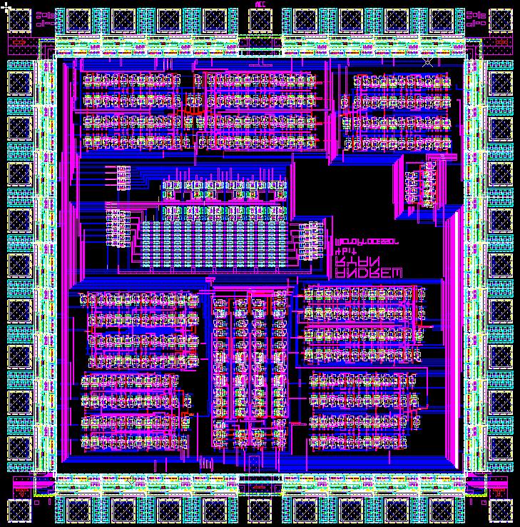
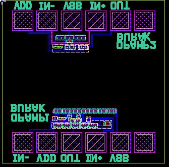
16 OVERALL CHIP LAYOUT The test chip is divided into nine cells each 5 mm by 5 mm. The cells are divided into 36 individual tiny cells each 800 µm by 800 µm in size plus 200 µm sawing streets. Most structures fit into the tiny cells including a 12 probe pad layout for probe card testing. The overall chip size is µm by 14800µm plus 200 µm sawing street to give x and y step size of 15 mm by 15 mm. (14800,14800) Page 16

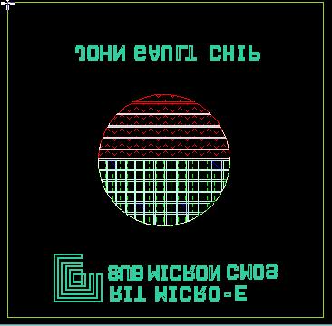
17 JOHN GALT CMOS TESTCHIP 2009 Page 17
18 4-BIT MICROPROCESSOR Page 18

19 ANALOG TO DIGITAL CONVERTER Output Register Comp Ref Buf Successive Approximation Register DAC Page 19

20 TINY CELL 800µm by 800µm 36 x 9 = 324 Page 20
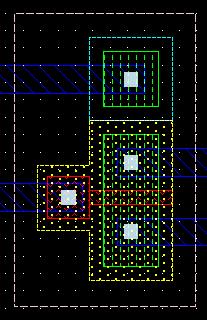
21 STRUCTURES FOR FAB PROCESS & EVALUATION Alignment Structures Overlay and Resolution Structures Big areas for measurement (Big Transistors) SEM Structures CC Chains Serpentines and Fingers for M1-M2 open and shorts Van Der Pauw s CBKR s NMOS and PMOS Transistors of Various Sizes Fully Scaled Sub-Micron Transistors Field Oxide Transistors Ring Oscillators Package Test Structures Page 21

22 ALIGNMENT KEYS On First Level Nwell or STI On Metal 1 Page 22


23 RESOLUTION AND OVERLAY Page 23


24 BIG NMOS AND PMOS FETS L/W = 100µm/150µm Big enough for easy Nanospec Measurements Page 24


25 FIELD OXIDE NMOS AND PMOS FET S Page 25


26 NMOS AND PMOS TRANSISTORS 1/4 2/4 4/4 8/4 16/4 32/4 1/8 2/8 4/8 8/8 16/8 32/8 1/32 2/32 4/32 8/32 16/32 32/32 Various L/W Ratios NMOS 2/8 PMOS 2/8 Page 26

27 FULLY SCALED SUB MICRON TRANSISTORS Page 27
28 RING OSCILLATORS AND SEM STRUCTURES 17 Stage Un-buffered Output L/W=2/30 Buffered Output L/W 8/16 4/16 2/16 73 Stage 37 Stage SEM Structures CMOS Inverter Crossection Page 28


29 VAN DER PAUWS AND CBKR s NWELL PWELL N+ P+ N-POLY M1 P-POLY M2 2µm M1toPoly 2µm M1toM2 2µm M1toP+ 2µm M1toP+ 2µm M1toN+ 2µm M1toN+ 4µm M1toPoly 4µm M1toM2 4µm M1toP+ 4µm M1toP+ 4µm M1toN+ 4µm M1toN+ Page 29


30 SERPENTINES, COMBS, AND VIA CHAINS To evaluate metal1, metal2, CC and Via layer quality. Page 30
31 RING OSCILLATORS AND SEM STRUCTURES 17 Stage Un-buffered Output L/W=2/30 Buffered Output L/W 8/16 4/16 2/16 73 Stage 37 Stage SEM Structures CMOS Inverter Crossection Page 31

32 SEM CROSSECTION OF INVERTER NMOSFET PMOSFET P-well N-well Need to polish, etch then SEM Page 32
33 SENSORS Interdigitated and Plate Capacitors Diodes and Heaters Resistors Photovoltaic Cells, 1x, 2x, 4x Two side by side pn diode sensors for differential readout Page 33

34 CAPACITORS M2 M1 M1 to M2 M1 to Poly 120 Fingers gives ~0.3 pf 670µm/470µm Plate ~3 pf Page 34

35 DIODES AND HEATERS Poly Heater on top of Diodes Integrated series well resistor. Page 35


36 RESISTORS P+ in Nwell N+ in Pwell Page 36


37 RESISTORS Nwell in P substrate 6 different Resistor Designs N+ Poly Page 37


38 PHOTOVOLTAIC DEVICES 8 cell battery dual cells single cell P+ in Nwell ~350µm by ~350µm Page 38

39 BIG PHOTO VOLTAIC CELL Page 39
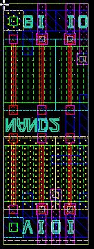
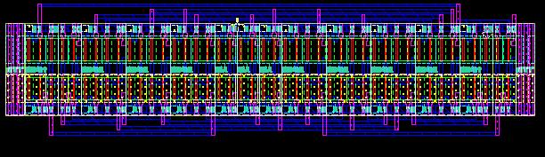
40 DIGITAL CIRCUITS Primitive Cells INVERTER, NAND2,3,4, NOR2,3,4, NULL Basic Cells XOR, MUX, DEMUX, ENCODER, DECODER FULL ADDER, FLIP FLOPS Macro Cells BINARY COUNTER SRAM Page 40

41 PRIMITIVE CELLS WITH PADS INV/NOR4 NOR3/NAND2 NOR2/NAND3 INV/NAND4 Page 41


42 CMOS INVERTER Vin Vout Vin +V Idd PMOS Vout NMOS CMOS TRUTH TABLE VIN VOUT W = 40 µm Ldrawn = 2.5µm Lpoly = 1.0µm Leff = 0.35 µm Page 42


43 PRIMITIVE CELLS Page 43


44 BASIC DIGITAL CELLS WITH PADS Decoder Multiplexer XOR Full Adder Encoder Decoder Demux Edge Triggered D FF JK FF Page 44

45 4 TO 1 MULTIPLEXER I 0 A I 1 I 2 Q B I 3 Page 45

46 BASIC CELL XOR Input A Port in Input B A B A B XOR Port out Port in A AB XOR = A B+AB B XOR Page 46

47 XOR Page 47

48 FULL ADDER Page 48

49 1 TO 4 DEMULTIPLEXER I A B Q 0 Q 1 Q 2 Q 3 Page 49

50 DECODER A Q 0 Q 1 B Q 2 Q 3 Page 50

51 Q 0 Q 1 Q 2 Q n Digital Encoder Coded Output Lines 512 inputs can be coded into 9 lines which is a more dramatic benefit ENCODER A B C D Q0 Q A B Q 1 C D No Connection Q 2 Page 51

52 EDGE TRIGGERED D TYPE FLIP FLOP Page 52
53 JK FLIP FLOP Page 53
54 T-TYPE FILP-FLOP TOGGEL FLIP FLOP T Q QBAR Q: Toggles High and Low with Each Input T Qn-1 Q Page 54
55 Input Pulses BINARY COUNTER USING T TYPE FLIP FLOPS T A T B Tc A A B B C C T A State Table for Binary Counter Present Next F-F State State Inputs B A B C T A T B T C Qn-1 C Q TOGGEL FLIP FLOP A BC T A 0 A BC T B 0 A BC T C 1 Page 55

56 3-BIT BINARY COUNTER WITH D FLIP FLOPS Page 56
57 MACROCELLS Binary Counter SRAM Page 57

58 3-BIT BINARY COUNTER/SHIFT REGISTER Binary Counter Serial Output Asynchronous Reset Count Up Enable Shift Out Clock Input Count Up Clock Input Start Bit and Stop Bit Page 58


59 8-BIT BINARY COUNTER Page 59

60 8-BIT BINARY COUNTER WITH PADS Page 60

61 SRAM 1 M5 M2 2 Q 5 Vd d W L 4 M4 3 6 Q M6 BL M1 M3 BL GN D Page 61
62 ANALOG AND MIXED MODE CIRCUITS Operational Amplifier Inverter with Hysteresis RC Oscillator Two Phase Clock Analog Switches Voltage Doubler, Tripler Analog Multiplexer Comparator with Hysteresis A-to-D D-to-A OTA, Biquad Filter, Elliptic Filter Programmable Binary Weighted Resistors Page 62
63 SPICE PARAMETERS FOR SUB-CMOS PROCESS *This file is called: RIT_MICROE_MODELS.TXT * * FROM DR. FULLER S SPREADSHEET WITH VT0=0.75.MODEL RITSUBN49 NMOS (LEVEL=49 VERSION=3.1 CAPMOD=2 MOBMOD=1 +TOX=1.5E-8 XJ=1.84E-7 NCH=1.45E17 NSUB=5.33E16 XT=8.66E-8 NSS=3E11 +XWREF=2.0E-7 XLREF=2.95E-7 VTH0=0.75 U0= 950 WINT=2.0E-7 LINT=1.84E-7 +NGATE=5E20 RSH=1082 JS=3.23E-8 JSW=3.23E-8 CJ=6.8E-4 MJ=0.5 PB=0.95 +CJSW=1.26E-10 MJSW=0.5 PBSW=0.95 PCLM=5 +CGS0=3.4E-10 CGD0=3.4E-10 CGB0=5.75E-10) * * FROM DR. FULLER S SPREADSHEET WITH VT0=-0.75.MODEL RITSUBP49 PMOS (LEVEL=49 VERSION=3.1 CAPMOD=2 MOBMOD=1 +TOX=1.5E-8 XJ=2.26E-7 NCH=7.12E16 NSUB=3.16E16 XT=8.66E-8 NSS=3E11 PCLM=5 +XWREF= 2.0E-7 XLREF=3.61E-7 VTH0=-0.75 U0= WINT=2.0E-7 LINT=2.26E-7 +RSH=1347 JS=3.51E-8 JSW=3.51E-8 CJ=5.28E-4 MJ=0.5 PB=0.94 +CJSW=1.19E-10 MJSW=0.5 PBSW=0.94 NGATE=5E20 +CGS0=4.5E-10 CGD0=4.5E-10 CGB0=5.75E-10) * Page 63

64 OPERATIONAL AMPLIFIER Version 1 Page 64
65 VERSION 1 OPERATIONAL AMPLIFIER +V M11 M10 M9 M8 L/W 80/20 80/20 80/20 20/40 5 Vin- M3 2 M1 M5 M4 20/40 20/40 M2 20/30 20/ /40 4 Vin+ 3 M6 M7 20/30 9 Vout 20/40 -V 20 p-well CMOS dimensions L/W (µm/µm) Page 65

66 SPICE ANALYSIS OF OP AMP VERSION 2.inclrit_sub_param.txt m cmosn w=9u l=5u nrd=1 nrs=1 ad=45p pd=28u as=45p ps=28u m cmosn w=9u l=5u nrd=1 nrs=1 ad=45p pd=28u as=45p ps=28u m cmosp w=21u l=5u nrd=1 nrs=1 ad=102p pd=50u as=102p ps=50u m cmosp w=21u l=5u nrd=1 nrs=1 ad=102p pd=50u as=102p ps=50u m cmosn w=40u l=5u nrd=1 nrs=1 ad=205p pd=90u as=205p ps=90u m cmosp w=190u l=5u nrd=1 nrs=1 ad=950p pd=400u as=950p ps=400u m cmosn w=190u l=5u nrd=1 nrs=1 ad=950p pd=400u as=950p ps=400u m cmosn w=40u l=5u nrd=1 nrs=1 ad=205p pd=90u as=205p ps=90u vdd vss cprobe p Rprobe 2 0 1meg cc p mr cmosp w=6u l=10u nrd=1 nrs=1 ad=200p pd=60u as=200p ps=60u mr cmosp w=6u l=10u nrd=1 nrs=1 ad=200p pd=60u as=200p ps=60u *************** ***dc open loop gain********* ************* vi vi *.dc vi u.dc vi m *****open loop frequency characteristics***** *vi *vi dc 0 ac 1u *.ac dec g.end 13.5kV/V gain Page 66

67 INVERTER WITH HYSTERESIS RC OSCILLATOR Page 67

68 TWO PHASE CLOCK CLOCK R t 2 Q F1 t 1 CLOCKBAR S t 3 F2 Page 68
69 WINSPICE SIMULATION FOR VERSION TWO + BUFFERS CLOCK R t 2 F1 t 1 CLOCKBAR S t 3 F2 Next Design add buffers Page 69

70 TWO PHASE CLOCK WITH BUFFERS Page 70

71 ANALOG SWITCH Vin S D D S Vout +V 0-5V Logic Control +5 -V Page 71

72 VOLTAGE DOUBLER F2 F2 F1 F1 C Load R Load C1 Vdd F1 F1 C1 F2 Voltage Tripler Page 72
73 OPERATIONAL TRANSCONDUCTANCE AMPLIFIER Va + Vb - Va + Vb V+ V- Ibias Iout Iout gm(va-vb) 5 Vin- M5 M3 2 M1 +V M4 12/30 12/30 12/30 12/30 Vref - Ibias 1 M2 12/30 -V CMOS Realization 4 Vin+ 12/30 M3 M4 Note: gm is set by Ibias Iout Page 73
74 BIQUAD FILTER V+ V+ V+ + - g m1 + - gm2 + - g m3 Vout V- Ibias V+ V- Ibias V+ V- Ibias C2 VB + VA + - g m5 C1 - g m4 V- Ibias VC V- Ibias Page 74
75 BIQUAD FILTER V out = (s 2 C 1 C 2 V c + s C 1 g m4 V b + g m2 g m5 V a )/(s 2 C 1 C 2 + sc 1 g m3 +g m2 g m1 ) This filter can be used as a low-pass, high-pass, bandpass, bandrejection and all pass filter. Depending on the C and gm values a Butterworth, Chebyshev, Elliptic or any other configuration can be achieved For example: let Vc=Vb=0 and Va=Vin, also let all g m be equal, then Vout = Vin / (s 2 C 1 C 2 / g m g m + sc 1 /g m + 1) which is a second order low pass filter with corner frequency at ω c = g m / C 1 C 2 and Q = C 2 /C 1 Page 75

76 OTA, BIQUAD ELLIPTIC FILTER gain LOWPASS FILTERS Butterworth Elliptic Chebycheff frequency Page 76
77 3 BIT ANALOG TO DIGITAL CONVERTER 8V +V Vin 7V 6V 5V 4V 3V 2V 1V 3.5V Comparators Segment Detector Decoding Logic Page 77

78 3 BIT ANALOG TO DIGITAL CONVERTER Page 78
79 ANALOG MULTIPLEXER 128 PHOTODIODES D1 D2 D3 D4 D5 D6 D7 D8 SWITCHES A A B B C C Analog out A.G 7 BIT COUNTER Sync Sync pulse (at B) Clock Reset Page 79

80 8 TO 1 ANALOG MUX Page 80
81 3 BIT D TO A Vref b1 b1 b2 b3 b3 b2 MSB Vout LSB Page 81

82 3 BIT D TO A Page 82
83 PROJECTS Wireless Capacitive Sensor MEMS Pressure Sensor Spectro Photometer Hearing Aid CCD CCD Imager Page 83
84 WIRELESS CAPACITIVE SENSOR PROJECT RC Oscillator RC Oscillator 2.4 khz 5 Hz CTS 5 Hz Stop Bit 3 V TX SCLK RCLK RX 1 10-bit (Left) Shift Register 1 RTS Bluetooth Serial RF Link Start Bit 0 0 CCKEN RCO CCLK 0 8-bit Binary Counter 0 0 RCLK CCLR Rochester Institute Internal of Technology Counter RC Oscillator Sensor Page 84

85 WIRELESS CAPACITIVE SENSOR PROJECT Page 85

86 MEMS PRESSURE SENSOR Page 86
87 SPECTRO PHOTOMETER PROJECT 7 B it Counter A B C A B C Reset C Internal Rf 100 pf Vout Ri D7 D0 Page 87

88 SOLDER BUMP TEST CHIP 1000µm center-to-center 225µm diameter circle Under bump metal is Cr/Ni and is defined by a lift-off lithography. The solder is printed using a 150um photoresist and solder paste. (or 500um solder ball is placed over circle) Page 88

89 LOGO AND ACKNOWLEDGEMENTS Page 89
90 REFERENCES 1. Introduction to VLSI Systems, Carver Mead and Lynn Conway, Addison- Wesley Publishing Company, Analog VLSI Design - nmos and CMOS Malcomb R. Haskard and Ian C. May, Prentice Hall Publishing Company. 3. Principles of CMOS VLSI Design - A Systems Perspective, Neil Weste, and Kaman Eshraghian, Addison-Wesley Publishing Company, CMOS Analog Circuit Design, Phillip E. Allen and Douglas R. Holberg, Holt, Rinehart and Winston Publishers, Analysis and Design of Analog Integrated Circuits, Paul R. Gray and Robert G. Meyer, John Wiley and Sons Publishers, Switched Capacitor Circuits, Phillip E. Allen and Edgar Sanchez-Sinencio, Van Nostrand Reinhold Publishers, Active Filter Design Using Operational Transconductance Amplifiers: A Tutorial, Randall L. Geiger and Edgar Sanchez-Sinencio, IEEE Circuits and Devices Magazine, March 1985, pg Digital Principles and Design, Donald Givone, 2003, pg MOSIS SCMOS at Texas Instruments, Data Sheet for inverter with hysteresis. Page 90
91 HOMEWORK 1. Calculate the expected values of some of the resistor test structures. 2. Calculate the expected values of some of the capacitor test structures. Page 91
Basic Analog Electronic Circuits Dr. Lynn Fuller
 ROCHESTER INSTITUTE OF TECHNOLOGY MICROELECTRONIC ENGINEERING Dr. Lynn Fuller Webpage: http://people.rit.edu/lffeee 82 Lomb Memorial Drive Rochester, NY 146235604 Tel (585) 4752035 Email: Lynn.Fuller@rit.edu
NMOS Inverter Lab ROCHESTER INSTITUTE OF TECHNOLOGY MICROELECTRONIC ENGINEERING. NMOS Inverter Lab
 ROCHESTER INSTITUTE OF TECHNOLOGY MICROELECTRONIC ENGINEERING NMOS Inverter Lab Dr. Lynn Fuller Webpage: http://people.rit.edu/lffeee/ 82 Lomb Memorial Drive Rochester, NY 14623-5604 Tel (585) 475-2035
Electronic Circuit Casebook. Dr. Lynn Fuller
 ROCHESTER INSTITUTE OF TECHNOLOGY MICROELECTRONIC ENGINEERING Electronic Circuit Casebook Dr. Lynn Fuller Webpage: http://people.rit.edu/lffeee 82 Lomb Memorial Drive Rochester, NY 146235604 Tel (585)
MOS Inverters Dr. Lynn Fuller Webpage:
 ROCHESTER INSTITUTE OF TECHNOLOGY MICROELECTRONIC ENGINEERING MOS Inverters Webpage: http://people.rit.edu/lffeee 82 Lomb Memorial Drive Rochester, NY 14623-5604 Tel (585) 475-2035 Email: Lynn.Fuller@rit.edu
Team Galt Real Microsystems
 ROCHESTER INSTITUTE OF TECHNOLOGY MICROELECTRONIC ENGINEERING Team Galt Real Microsystems Dr. Lynn Fuller, Ivan Puchades, Heidi Purrington, Murat Baylav, Jake Leveto, Ellen Sedlack, Tal Nagourney, Christian
Team Galt Real Microsystems
 ROCHESTER INSTITUTE OF TECHNOLOGY MICROELECTRONIC ENGINEERING Team Galt Real Microsystems Dr. Lynn Fuller, Dr. Ivan Puchades, Heidi Purrington, Murat Baylav, Jake Leveto, Ellen Sedlack, Tal Nagourney,
Selected Filter Circuits Dr. Lynn Fuller
 ROCHESTER INSTITUTE OF TECHNOLOGY MICROELECTRONIC ENGINEERING Dr. Lynn Fuller Webpage: http://people.rit.edu/lffeee Electrical and 82 Lomb Memorial Drive Rochester, NY 146235604 Tel (585) 4752035 Email:
Differential Amplifier with Current Source Bias and Active Load
 Technical Memo: Differential Amplifier with Current Source Bias and Active Load Introduction: From: Dr. Lynn Fuller, Professor, Electrical and Microelectronic Engineering, Rochester Institute of Technology
Selected Analog Electronic Circuits Dr. Lynn Fuller
 ROCHESTER INSTITUTE OF TECHNOLOGY MICROELECTRONIC ENGINEERING Selected Analog Electronic Circuits Dr. Lynn Fuller Webpage: http://people.rit.edu/lffeee 82 Lomb Memorial Drive Rochester, NY 146235604 Tel
Introduction to LTSPICE Dr. Lynn Fuller Electrical and Microelectronic Engineering
 ROCHESTER INSTITUTE OF TECHNOLOGY MICROELECTRONIC ENGINEERING Introduction to LTSPICE Dr. Lynn Fuller Electrical and 82 Lomb Memorial Drive Rochester, NY 14623-5604 Tel (585) 475-2035 Fax (585) 475-5041
Diode Sensor Lab. Dr. Lynn Fuller
 ROCHESTER INSTITUTE OF TECHNOLOGY MICROELECTRONIC ENGINEERING Diode Sensor Lab Dr. Lynn Fuller Webpage: http://people.rit.edu/lffeee 82 Lomb Memorial Drive Rochester, NY 14623-5604 Tel (585) 475-2035 Fax
EEEE 381 Electronics I
 EEEE 381 Electronics I Lab #5: Two-Stage CMOS Op-Amp Oeriew In this lab we will expand on the work done in Lab #4, which introduced the actiely-loaded differential pair. A second stage that is comprised
Laboratory on Filter Circuits Dr. Lynn Fuller
 ROCHESTER INSTITUTE OF TECHNOLOGY MICROELECTRONIC ENGINEERING Laboratory on Filter Circuits Dr. Lynn Fuller Webpage: http://people.rit.edu/lffeee 82 Lomb Memorial Drive Rochester, NY 14623-5604 Tel (585)
Static Random Access Memory - SRAM Dr. Lynn Fuller Webpage:
 ROCHESTER INSTITUTE OF TECHNOLOGY MICROELECTRONIC ENGINEERING Static Random Access Memory - SRAM Dr. Lynn Fuller Webpage: http://people.rit.edu/lffeee 82 Lomb Memorial Drive Rochester, NY 14623-5604 Email:
Introduction to Modeling MOSFETS in SPICE
 ROCHESTER INSTITUTE OF TECHNOLOGY MICROELECTRONIC ENGINEERING Introduction to Modeling MOSFETS in SPICE Dr. Lynn Fuller Electrical and 82 Lomb Memorial Drive Rochester, NY 14623-5604 Dr. Fuller s Webpage:
Introduction to the Long Channel MOSFET. Dr. Lynn Fuller
 ROCHESTER INSTITUTE OF TECHNOLOGY MICROELECTRONIC ENGINEERING Introduction to the Long Channel MOSFET Dr. Lynn Fuller Webpage: http://people.rit.edu/lffeee Electrical and 82 Lomb Memorial Drive Rochester,
PHYSICAL STRUCTURE OF CMOS INTEGRATED CIRCUITS. Dr. Mohammed M. Farag
 PHYSICAL STRUCTURE OF CMOS INTEGRATED CIRCUITS Dr. Mohammed M. Farag Outline Integrated Circuit Layers MOSFETs CMOS Layers Designing FET Arrays EE 432 VLSI Modeling and Design 2 Integrated Circuit Layers
PMOS Testing at. Rochester Institute of Technology. Dr. Lynn Fuller
 ROCHESER INSIUE OF ECHNOLOGY MICROELECRONIC ENGINEERING PMOS esting at Dr. Lynn Fuller webpage: http://www.rit.edu/~lffeee 82 Lomb Memorial Drive Rochester, NY 14623-5604 el (585) 475-2035 Fax (585) 475-5041
Advanced MOSFET Basics. Dr. Lynn Fuller
 ROCHESTER INSTITUTE OF TECHNOLOGY MICROELECTRONIC ENGINEERING Advanced MOSFET Basics Dr. Lynn Fuller Webpage: http://people.rit.edu/lffeee 82 Lomb Memorial Drive Rochester, NY 14623-5604 Tel (585) 475-2035
Power Conditioning Electronics Dr. Lynn Fuller Webpage:
 ROCHESTER INSTITUTE OF TECHNOLOGY MICROELECTRONIC ENGINEERING Power Conditioning Electronics Dr. Lynn Fuller Webpage: http://people.rit.edu/lffeee 82 Lomb Memorial Drive Rochester, NY 14623-5604 Email:
Basic Layout Techniques
 Basic Layout Techniques Rahul Shukla Advisor: Jaime Ramirez-Angulo Spring 2005 Mixed Signal VLSI Lab Klipsch School of Electrical and Computer Engineering New Mexico State University Outline Transistor
High Voltage and MEMS Process Integration
 ROCHESTER INSTITUTE OF TECHNOLOGY MICROELECTRONIC ENGINEERING High Voltage and MEMS Process Integration Dr. Lynn Fuller and Dr. Ivan Puchades webpage: http://people.rit.edu/lffeee Electrical and Microelectronic
Introduction to Electronics. Dr. Lynn Fuller
 ROCHESTER INSTITUTE OF TECHNOLOGY MICROELECTRONIC ENGINEERING Introduction to Electronics Dr. Lynn Fuller Webpage: http://www.rit.edu/~lffeee 82 Lomb Memorial Drive Rochester, NY 14623-5604 Tel (585) 475-2035
A MOS VLSI Comparator
 A MOS VLSI Comparator John Monforte School of Music University of Miami, Coral Gables, FL. USA Jayant Datta Department of Electrical Engineering University of Miami, Coral Gables, FL. USA ABSTRACT A comparator
EE 330 Homework 5 Fall 2016 (Due Friday Sept 23)
") EE 330 Homework 5 Fall 2016 (Due Friday Sept 23) Assume the CMOS process is characterized by model parameters VTH=1V and µcox=100µa/v 2. If any other model parameters are needed, use the measured parameters
EE 330 Homework 5 Fall 2016 (Due Friday Sept 23) Assume the CMOS process is characterized by model parameters VTH=1V and µcox=100µa/v 2. If any other model parameters are needed, use the measured parameters
DESIGN OF A 4-BiT PMOS PARALLEL COMPARATOR AID CONVERTER. Amel Gaddo 5th year Microelectronic Engineering Student Rochester Institute of TechnologY
 DESIGN OF A 4-BiT PMOS PARALLEL COMPARATOR AID CONVERTER Amel Gaddo 5th year Microelectronic Engineering Student Rochester Institute of TechnologY ABSTRACT INTRODUCTION This project dealt with the design
Advanced MOSFET Basics. Dr. Lynn Fuller
 ROCHESTER INSTITUTE OF TECHNOLOGY MICROELECTRONIC ENGINEERING Advanced MOSFET Basics Dr. Lynn Fuller Webpage: http://people.rit.edu/lffeee 82 Lomb Memorial Drive Rochester, NY 14623-5604 Tel (585) 475-2035
MEMS Signal Conditioning Circuits Dr. Lynn Fuller Electrical and Microelectronic Engineering
 ROCHESTER INSTITUTE OF TECHNOLOGY MICROELECTRONIC ENGINEERING MEMS Signal Conditioning Circuits Dr. Lynn Fuller Electrical and 82 Lomb Memorial Drive Rochester, NY 146235604 Email: Lynn.Fuller@rit.edu
Final for EE 421 Digital Electronics and ECG 621 Digital Integrated Circuit Design Fall, University of Nevada, Las Vegas
 Final for EE 421 Digital Electronics and ECG 621 Digital Integrated Circuit Design Fall, University of Nevada, Las Vegas NAME: Show your work to get credit. Open book and closed notes. Unless otherwise
Single Supply Op Amp Circuits Dr. Lynn Fuller Webpage:
 ROCHESTER INSTITUTE OF TECHNOLOGY MICROELECTRONIC ENGINEERING Single Supply Op Amp Circuits Dr. Lynn Fuller Webpage: http://people.rit.edu/lffeee 82 Lomb Memorial Drive Rochester, NY 146235604 Tel (585)
Fan in: The number of inputs of a logic gate can handle.
 Subject Code: 17333 Model Answer Page 1/ 29 Important Instructions to examiners: 1) The answers should be examined by key words and not as word-to-word as given in the model answer scheme. 2) The model
problem grade total
 Fall 2005 6.012 Microelectronic Devices and Circuits Prof. J. A. del Alamo Name: Recitation: November 16, 2005 Quiz #2 problem grade 1 2 3 4 total General guidelines (please read carefully before starting):
UMAINE ECE Morse Code ROM and Transmitter at ISM Band Frequency
 UMAINE ECE Morse Code ROM and Transmitter at ISM Band Frequency Jamie E. Reinhold December 15, 2011 Abstract The design, simulation and layout of a UMAINE ECE Morse code Read Only Memory and transmitter
EEEE 381 Electronics I
 EEEE 381 Electrnics I Lab #4: MOSFET Differential Pair with Active Lad Overview The differential amplifier is a fundamental building blck in electrnic design. The bjective f this lab is t examine the vltage
ENEE307 Lab 7 MOS Transistors 2: Small Signal Amplifiers and Digital Circuits
 ENEE307 Lab 7 MOS Transistors 2: Small Signal Amplifiers and Digital Circuits In this lab, we will be looking at ac signals with MOSFET circuits and digital electronics. The experiments will be performed
FUTURE PROSPECTS FOR CMOS ACTIVE PIXEL SENSORS
 FUTURE PROSPECTS FOR CMOS ACTIVE PIXEL SENSORS Dr. Eric R. Fossum Jet Propulsion Laboratory Dr. Philip H-S. Wong IBM Research 1995 IEEE Workshop on CCDs and Advanced Image Sensors April 21, 1995 CMOS APS
R & D Electronics DIGITAL IC TRAINER. Model : DE-150. Feature: Object: Specification:
 DIGITAL IC TRAINER Model : DE-150 Object: To Study the Operation of Digital Logic ICs TTL and CMOS. To Study the All Gates, Flip-Flops, Counters etc. To Study the both the basic and advance digital electronics
Laboratory 1 Single-Stage MOSFET Amplifier Analysis and Design Due Date: Week of February 20, 2014, at the beginning of your lab section
 Laboratory 1 Single-Stage MOSFET Amplifier Analysis and Design Due Date: Week of February 20, 2014, at the beginning of your lab section Objective To analyze and design single-stage common source amplifiers.
Assoc. Prof. Dr. Burak Kelleci
 DEPARTMENT OF ELECTRICAL &ELECTRONICS ENGINEERING ANALOG-TO-DIGITAL AND DIGITAL- TO-ANALOG CONVERTERS Assoc. Prof. Dr. Burak Kelleci Fall 2018 OUTLINE Nyquist-Rate DAC Thermometer-Code Converter Hybrid
Modeling MOS Transistors. Prof. MacDonald
 Modeling MOS Transistors Prof. MacDonald 1 Modeling MOSFETs for simulation l Software is used simulate circuits for validation l Original program SPICE UC Berkeley Simulation Program with Integrated Circuit
PMOS Digital Testing at Rochester Institute of Technology
 1 PMOS Digital Testing at Rochester Institute of Technology Dr. Lynn Fuller, Adam Wardas webpage: http://www.rit.edu/lffeee Microelectronic Engineering Rochester Institute of Technology 82 Lomb Memorial
Dr. Lynn Fuller, Ivan Puchades
 ROCHESTER INSTITUTE OF TECHNOLOGY MICROELECTRONIC ENGINEERING Bulk Micromachined Laboratory Project Dr. Lynn Fuller, Ivan Puchades Motorola Professor 82 Lomb Memorial Drive Rochester, NY 14623-5604 Tel
ECE 5745 Complex Digital ASIC Design Topic 2: CMOS Devices
 ECE 5745 Complex Digital ASIC Design Topic 2: CMOS Devices Christopher Batten School of Electrical and Computer Engineering Cornell University http://www.csl.cornell.edu/courses/ece5950 Simple Transistor
Lecture 020 ECE4430 Review II (1/5/04) Page 020-1
 Page 020-1") Lecture 020 ECE4430 Review II (1/5/04) Page 020-1 LECTURE 020 ECE 4430 REVIEW II (READING: GHLM - Chap. 2) Objective The objective of this presentation is: 1.) Identify the prerequisite material as taught
Lecture 020 ECE4430 Review II (1/5/04) Page 020-1 LECTURE 020 ECE 4430 REVIEW II (READING: GHLM - Chap. 2) Objective The objective of this presentation is: 1.) Identify the prerequisite material as taught
An Analog Phase-Locked Loop
 1 An Analog Phase-Locked Loop Greg Flewelling ABSTRACT This report discusses the design, simulation, and layout of an Analog Phase-Locked Loop (APLL). The circuit consists of five major parts: A differential
ECEN474/704: (Analog) VLSI Circuit Design Fall 2016
 VLSI Circuit Design Fall 2016") ECEN474/704: (Analog) VLSI Circuit Design Fall 2016 Lecture 1: Introduction Sam Palermo Analog & Mixed-Signal Center Texas A&M University Announcements Turn in your 0.18um NDA form by Thursday Sep 1 No
ECEN474/704: (Analog) VLSI Circuit Design Fall 2016 Lecture 1: Introduction Sam Palermo Analog & Mixed-Signal Center Texas A&M University Announcements Turn in your 0.18um NDA form by Thursday Sep 1 No
Probes and Electrodes Dr. Lynn Fuller Webpage:
 ROCHESTER INSTITUTE OF TECHNOLOGY MICROELECTRONIC ENGINEERING Probes and Electrodes Dr. Lynn Fuller Webpage: http://people.rit.edu/lffeee 82 Lomb Memorial Drive Rochester, NY 14623-5604 Tel (585) 475-2035
MEMS Microphone Design and Signal Conditioning Dr. Lynn Fuller, Erin Sullivan Webpage:
 ROCHESTER INSTITUTE OF TECHNOLOGY MICROELECTRONIC ENGINEERING MEMS Microphone Design and Signal Conditioning, Erin Sullivan Webpage: http://people.rit.edu/lffeee 82 Lomb Memorial Drive Rochester, NY 14623-5604
High Temperature Mixed Signal Capabilities
 High Temperature Mixed Signal Capabilities June 29, 2017 Product Overview Features o Up to 300 o C Operation o Will support most analog functions. o Easily combined with up to 30K digital gates. o 1.0u
CMOS Operational Amplifier
 The George Washington University Department of Electrical and Computer Engineering Course: ECE218 Instructor: Mona E. Zaghloul Students: Shunping Wang Yiping (Neil) Tsai Data: 05/14/07 Introduction In
SOLIMAN A. MAHMOUD Department of Electrical Engineering, Faculty of Engineering, Cairo University, Fayoum, Egypt
 Journal of Circuits, Systems, and Computers Vol. 14, No. 4 (2005) 667 684 c World Scientific Publishing Company DIGITALLY CONTROLLED CMOS BALANCED OUTPUT TRANSCONDUCTOR AND APPLICATION TO VARIABLE GAIN
EE584 Introduction to VLSI Design Final Project Document Group 9 Ring Oscillator with Frequency selector
 EE584 Introduction to VLSI Design Final Project Document Group 9 Ring Oscillator with Frequency selector Group Members Uttam Kumar Boda Rajesh Tenukuntla Mohammad M Iftakhar Srikanth Yanamanagandla 1 Table
Lecture 020 ECE4430 Review II (1/5/04) Page 020-1
 Page 020-1") Lecture 020 ECE4430 Review II (1/5/04) Page 020-1 LECTURE 020 ECE 4430 REVIEW II (READING: GHLM - Chap. 2) Objective The objective of this presentation is: 1.) Identify the prerequisite material as taught
Lecture 020 ECE4430 Review II (1/5/04) Page 020-1 LECTURE 020 ECE 4430 REVIEW II (READING: GHLM - Chap. 2) Objective The objective of this presentation is: 1.) Identify the prerequisite material as taught
Implementing a 5-bit Folding and Interpolating Analog to Digital Converter
 Implementing a 5-bit Folding and Interpolating Analog to Digital Converter Zachary A Pfeffer (pfefferz@colorado.edu) Department of Electrical and Computer Engineering University of Colorado, Boulder CO
Low Power Design of Successive Approximation Registers
 Low Power Design of Successive Approximation Registers Rabeeh Majidi ECE Department, Worcester Polytechnic Institute, Worcester MA USA rabeehm@ece.wpi.edu Abstract: This paper presents low power design
EE301 Electronics I , Fall
 EE301 Electronics I 2018-2019, Fall 1. Introduction to Microelectronics (1 Week/3 Hrs.) Introduction, Historical Background, Basic Consepts 2. Rewiev of Semiconductors (1 Week/3 Hrs.) Semiconductor materials
Lab 2 Revisited Exercise
 Lab 2 Revisited Exercise +15V 100k 1K 2N2222 Wire up led display Note the ground leads LED orientation 6.091 IAP 2008 Lecture 3 1 Comparator, Oscillator +5 +15 1k 2 V- 7 6 Vin 3 V+ 4 V o Notice that power
Analog IC Design and Fabrication
 Analog IC Design and Fabrication James Tom Microelectronic Engineering Rochester Institute of Technology Rochester, NY 14623 Abstract The purpose of this project was to test the performance of analog integrated
Lecture 0: Introduction
 Lecture 0: Introduction Introduction Integrated circuits: many transistors on one chip. Very Large Scale Integration (VLSI): bucketloads! Complementary Metal Oxide Semiconductor Fast, cheap, low power
IC Layout Design of 4-bit Universal Shift Register using Electric VLSI Design System
 IC Layout Design of 4-bit Universal Shift Register using Electric VLSI Design System 1 Raj Kumar Mistri, 2 Rahul Ranjan, 1,2 Assistant Professor, RTC Institute of Technology, Anandi, Ranchi, Jharkhand,
ELECTRONICS WITH DISCRETE COMPONENTS
 ELECTRONICS WITH DISCRETE COMPONENTS Enrique J. Galvez Department of Physics and Astronomy Colgate University WILEY John Wiley & Sons, Inc. ^ CONTENTS Preface vii 1 The Basics 1 1.1 Foreword: Welcome to
CMOS 65nm Process Monitor
 CMOS 65nm Process Monitor Final Report Fall Semester 2008 Prepared to partially fulfill the requirements for ECE401 Department of Electrical and Computer Engineering Colorado State University Fort Collins,
CMOS Instrumentation Amplifier with Offset Cancellation Circuitry for Biomedical Application
 CMOS Instrumentation Amplifier with Offset Cancellation Circuitry for Biomedical Application Author Mohd-Yasin, Faisal, Yap, M., I Reaz, M. Published 2006 Conference Title 5th WSEAS Int. Conference on
ECEN474: (Analog) VLSI Circuit Design Fall 2011
 VLSI Circuit Design Fall 2011") ECEN474: (Analog) VLSI Circuit Design Fall 2011 Lecture 1: Introduction Sebastian Hoyos Analog & Mixed-Signal Center Texas A&M University Analog Circuit Sequence 326 2 Why is Analog Important? [Silva]
ECEN474: (Analog) VLSI Circuit Design Fall 2011 Lecture 1: Introduction Sebastian Hoyos Analog & Mixed-Signal Center Texas A&M University Analog Circuit Sequence 326 2 Why is Analog Important? [Silva]
DIGITAL INTEGRATED CIRCUITS A DESIGN PERSPECTIVE 2 N D E D I T I O N
 DIGITAL INTEGRATED CIRCUITS A DESIGN PERSPECTIVE 2 N D E D I T I O N Jan M. Rabaey, Anantha Chandrakasan, and Borivoje Nikolic CONTENTS PART I: THE FABRICS Chapter 1: Introduction (32 pages) 1.1 A Historical
A Compact Folded-cascode Operational Amplifier with Class-AB Output Stage
 A Compact Folded-cascode Operational Amplifier with Class-AB Output Stage EEE 523 Advanced Analog Integrated Circuits Project Report Fuding Ge You are an engineer who is assigned the project to design
EC 1354-Principles of VLSI Design
 EC 1354-Principles of VLSI Design UNIT I MOS TRANSISTOR THEORY AND PROCESS TECHNOLOGY PART-A 1. What are the four generations of integrated circuits? 2. Give the advantages of IC. 3. Give the variety of
ECEN 720 High-Speed Links: Circuits and Systems. Lab3 Transmitter Circuits. Objective. Introduction. Transmitter Automatic Termination Adjustment
 1 ECEN 720 High-Speed Links: Circuits and Systems Lab3 Transmitter Circuits Objective To learn fundamentals of transmitter and receiver circuits. Introduction Transmitters are used to pass data stream
Nonlinear Macromodeling of Amplifiers and Applications to Filter Design.
 ECEN 622 Nonlinear Macromodeling of Amplifiers and Applications to Filter Design. By Edgar Sanchez-Sinencio Thanks to Heng Zhang for part of the material OP AMP MACROMODELS Systems containing a significant
Basic Fabrication Steps
 Basic Fabrication Steps and Layout Somayyeh Koohi Department of Computer Engineering Adapted with modifications from lecture notes prepared by author Outline Fabrication steps Transistor structures Transistor
Design and Layout of Two Stage High Bandwidth Operational Amplifier
 Design and Layout of Two Stage High Bandwidth Operational Amplifier Yasir Mahmood Qureshi Abstract This paper presents the design and layout of a two stage, high speed operational amplifiers using standard
Nonlinear Macromodeling of Amplifiers and Applications to Filter Design.
 ECEN 622(ESS) Nonlinear Macromodeling of Amplifiers and Applications to Filter Design. By Edgar Sanchez-Sinencio Thanks to Heng Zhang for part of the material OP AMP MACROMODELS Systems containing a significant
Design for MOSIS Education Program
 Design for MOSIS Education Program (Research) T46C-AE Project Title Low Voltage Analog Building Block Prepared by: C. Durisety, S. Chen, B. Blalock, S. Islam Institution: Department of Electrical and Computer
CMOS voltage controlled floating resistor
 INT. J. ELECTRONICS, 1996, VOL. 81, NO. 5, 571± 576 CMOS voltage controlled floating resistor HASSAN O. ELWAN², SOLIMAN A. MAHMOUD² AHMED M. SOLIMAN² and A new CMOS floating linear resistor circuit with
ECE4902 B2015 HW Set 1
 ECE4902 B2015 HW Set 1 Due in class Tuesday November 3. To make life easier on the graders: Be sure your NAME and ECE MAILBOX NUMBER are prominently displayed on the upper right of what you hand in. When
Microelectronics, BSc course
 Microelectronics, BSc course MOS circuits: CMOS circuits, construction http://www.eet.bme.hu/~poppe/miel/en/14-cmos.pptx http://www.eet.bme.hu The abstraction level of our study: SYSTEM + MODULE GATE CIRCUIT
Preface to Third Edition Deep Submicron Digital IC Design p. 1 Introduction p. 1 Brief History of IC Industry p. 3 Review of Digital Logic Gate
 Preface to Third Edition p. xiii Deep Submicron Digital IC Design p. 1 Introduction p. 1 Brief History of IC Industry p. 3 Review of Digital Logic Gate Design p. 6 Basic Logic Functions p. 6 Implementation
Analog CMOS Interface Circuits for UMSI Chip of Environmental Monitoring Microsystem
 Analog CMOS Interface Circuits for UMSI Chip of Environmental Monitoring Microsystem A report Submitted to Canopus Systems Inc. Zuhail Sainudeen and Navid Yazdi Arizona State University July 2001 1. Overview
COMBINATIONAL and SEQUENTIAL LOGIC CIRCUITS Hardware implementation and software design
 PH-315 COMINATIONAL and SEUENTIAL LOGIC CIRCUITS Hardware implementation and software design A La Rosa I PURPOSE: To familiarize with combinational and sequential logic circuits Combinational circuits
TECHNO INDIA BATANAGAR (DEPARTMENT OF ELECTRONICS & COMMUNICATION ENGINEERING) QUESTION BANK- 2018
 QUESTION BANK- 2018") TECHNO INDIA BATANAGAR (DEPARTMENT OF ELECTRONICS & COMMUNICATION ENGINEERING) QUESTION BANK- 2018 Paper Setter Detail Name Designation Mobile No. E-mail ID Raina Modak Assistant Professor 6290025725 raina.modak@tib.edu.in
TECHNO INDIA BATANAGAR (DEPARTMENT OF ELECTRONICS & COMMUNICATION ENGINEERING) QUESTION BANK- 2018 Paper Setter Detail Name Designation Mobile No. E-mail ID Raina Modak Assistant Professor 6290025725 raina.modak@tib.edu.in
LECTURE 7. OPERATIONAL AMPLIFIERS (PART 2)
") CIRCUITS by Ulaby & Maharbiz All rights reserved. Do not reproduce or distribute. LECTURE 7. OPERATIONAL AMPLIFIERS (PART 2) 07/16/2013 ECE225 CIRCUIT ANALYSIS All rights reserved. Do not copy or distribute.
CIRCUITS by Ulaby & Maharbiz All rights reserved. Do not reproduce or distribute. LECTURE 7. OPERATIONAL AMPLIFIERS (PART 2) 07/16/2013 ECE225 CIRCUIT ANALYSIS All rights reserved. Do not copy or distribute.
Hot Topics and Cool Ideas in Scaled CMOS Analog Design
 Engineering Insights 2006 Hot Topics and Cool Ideas in Scaled CMOS Analog Design C. Patrick Yue ECE, UCSB October 27, 2006 Slide 1 Our Research Focus High-speed analog and RF circuits Device modeling,
CS302 - Digital Logic Design Glossary By
 CS302 - Digital Logic Design Glossary By ABEL : Advanced Boolean Expression Language; a software compiler language for SPLD programming; a type of hardware description language (HDL) Adder : A digital
Multiplexer for Capacitive sensors
 DATASHEET Multiplexer for Capacitive sensors Multiplexer for Capacitive Sensors page 1/7 Features Very well suited for multiple-capacitance measurement Low-cost CMOS Low output impedance Rail-to-rail digital
GOVERNMENT OF KARNATAKA KARNATAKA STATE PRE-UNIVERSITY EDUCATION EXAMINATION BOARD II YEAR PUC EXAMINATION JULY-2012 SCHEME OF VALUATION
 GOVERNMENT OF KARNATAKA KARNATAKA STATE PRE-UNIVERSITY EDUCATION EXAMINATION BOARD II YEAR PUC EXAMINATION JULY-0 SCHEME OF VALUATION Subject Code: 40 Subject: PART - A 0. Which region of the transistor
2. (2 pts) What is the major reason static CMOS NAND gates are often preferred over static CMOS NOR gates?
 What is the major reason static CMOS NAND gates are often preferred over static CMOS NOR gates?") EE 330 Final Exam Spring 05 Name Instructions: Students may bring 3 pages of notes (3 front + 3 back) to this exam. There are 0 questions and 8 problems. There are two points allocated to each question.
EE 330 Final Exam Spring 05 Name Instructions: Students may bring 3 pages of notes (3 front + 3 back) to this exam. There are 0 questions and 8 problems. There are two points allocated to each question.
Volterra. VT1115MF Pulse Width Modulation (PWM) Controller. Partial Circuit Analysis
 Controller. Partial Circuit Analysis") Volterra VT1115MF Pulse Width Modulation (PWM) Controller Partial Circuit Analysis For questions, comments, or more information about this report, or for any additional technical needs concerning semiconductor
Volterra VT1115MF Pulse Width Modulation (PWM) Controller Partial Circuit Analysis For questions, comments, or more information about this report, or for any additional technical needs concerning semiconductor
Samsung S5K3L1YX Mp, 1/3.2 Inch Optical Format 1.12 µm Pixel Pitch Back Illuminated (BSI) CMOS Image Sensor
 CMOS Image Sensor") Samsung S5K3L1YX03 12.1 Mp, 1/3.2 Inch Optical Format 1.12 µm Pixel Pitch Back Illuminated (BSI) CMOS Image Sensor Circuit Analysis of Pixel Array, Row Drivers, Column Readouts, Ramp Generator, DPLL, MIPI
Samsung S5K3L1YX03 12.1 Mp, 1/3.2 Inch Optical Format 1.12 µm Pixel Pitch Back Illuminated (BSI) CMOS Image Sensor Circuit Analysis of Pixel Array, Row Drivers, Column Readouts, Ramp Generator, DPLL, MIPI
12-nm Novel Topologies of LPHP: Low-Power High- Performance 2 4 and 4 16 Mixed-Logic Line Decoders
 12-nm Novel Topologies of LPHP: Low-Power High- Performance 2 4 and 4 16 Mixed-Logic Line Decoders Mr.Devanaboina Ramu, M.tech Dept. of Electronics and Communication Engineering Sri Vasavi Institute of
ECEN689: Special Topics in High-Speed Links Circuits and Systems Spring 2012
 ECEN689: Special Topics in High-Speed Links Circuits and Systems Spring 2012 Lecture 5: Termination, TX Driver, & Multiplexer Circuits Sam Palermo Analog & Mixed-Signal Center Texas A&M University Announcements
EE : ELECTRICAL ENGINEERING Module 8 : Analog and Digital Electronics INDEX
 Pearl Centre, S.B. Marg, Dadar (W), Mumbai 400 028. Tel. 4232 4232 EE : ELECTRICAL ENGINEERING Module 8 : Analog and Digital Electronics Contents INDEX Sub Topics 1. Characteristics of Diodes, BJT & FET
d. Can you find intrinsic gain more easily by examining the equation for current? Explain.
 EECS140 Final Spring 2017 Name SID 1. [8] In a vacuum tube, the plate (or anode) current is a function of the plate voltage (output) and the grid voltage (input). I P = k(v P + µv G ) 3/2 where µ is a
UNIT III VLSI CIRCUIT DESIGN PROCESSES. In this chapter we will be studying how to get the schematic into stick diagrams or layouts.
 UNIT III VLSI CIRCUIT DESIGN PROCESSES In this chapter we will be studying how to get the schematic into stick diagrams or layouts. MOS circuits are formed on four basic layers: N-diffusion P-diffusion
Schottky Diode RF-Detector and Focused Ion Beam Post-Processing MURI Annual Review
 Schottky Diode RF-Detector and Focused Ion Beam Post-Processing MURI Annual Review Woochul Jeon, Todd Firestone, John Rodgers & John Melngailis University of Maryland. (consultations with Jake Baker Boise
Lecture 300 Low Voltage Op Amps (3/28/10) Page 300-1
 Page 300-1") Lecture 300 Low Voltage Op Amps (3/28/10) Page 300-1 LECTURE 300 LOW VOLTAGE OP AMPS LECTURE ORGANIZATION Outline Introduction Low voltage input stages Low voltage gain stages Low voltage bias circuits
Lecture 300 Low Voltage Op Amps (3/28/10) Page 300-1 LECTURE 300 LOW VOLTAGE OP AMPS LECTURE ORGANIZATION Outline Introduction Low voltage input stages Low voltage gain stages Low voltage bias circuits
Broadcom. BCM4334 Single Chip Dual-Band Combo Wireless Connectivity Device. Circuit Analysis of Wi-Fi Transceiver
 Broadcom BCM4334 Single Chip Dual-Band Combo Wireless Connectivity Device Circuit Analysis of Wi-Fi Transceiver 1891 Robertson Road, Suite 500, Ottawa, ON K2H 5B7 Canada Tel: 613.829.0414 Fax: 613.829.0515
Process Components. Process component
 What are PROCESS COMPONENTS? Input Transducer Process component Output Transducer The input transducer circuits are connected to PROCESS COMPONENTS. These components control the action of the OUTPUT components
Lecture 3: Logic circuit. Combinational circuit and sequential circuit
 Lecture 3: Logic circuit Combinational circuit and sequential circuit TRAN THI HONG HONG@IS.NAIST.JP Content Lecture : Computer organization and performance evaluation metrics Lecture 2: Processor architecture
Sticks Diagram & Layout. Part II
 Sticks Diagram & Layout Part II Well and Substrate Taps Substrate must be tied to GND and n-well to V DD Metal to lightly-doped semiconductor forms poor connection called Shottky Diode Use heavily doped
Development of a Radiation Tolerant 2.0 V standard cell library using a commercial deep submicron CMOS technology for the LHC experiments.
 Development of a Radiation Tolerant 2.0 V standard cell library using a commercial deep submicron CMOS technology for the LHC experiments. K. Kloukinas, F. Faccio, A. Marchioro, P. Moreira, CERN/EP-MIC,