Status of ITC-irst activities in RD50
|
|
|
- Meryl Robertson
- 6 years ago
- Views:
Transcription
1 Status of ITC-irst activities in RD50 M. Boscardin ITC-irst, Microsystem Division Trento, Italy
2 Outline Materials/Pad Detctors Pre-irradiated silicon INFN Padova and Institute for Nuclear Research of NASU, KieV; Detectors on MCz, Cz and Epitaxial silicon SMART collaboration: INFN of Bari, Firenze, Padova Perugia, Pisa and Trieste; New detectors Thin Detectors - INFN of Firenze and Padova; 3-D detectors Glasgow and CNM Barcelona.
 MCz material = No LTO and sintering")
3 Pre-irradiated material Layout BaBar detector masks (single side) Diode + test structure Silicon Fz <100> n-type 6 kω MCz <111> n-type Okmetic >500Ω Pre-irradiation Pre-irradiation by fast neutrons at Kiev reactor, fluence n/cm 2 annealing at a temperature of 850 C Polishing, lapping rocess Fz material = standard Irst (LTO, sintering@420 C) MCz material = No LTO and C.
4 Electrical Characterization Type n V dep (V) N eff (10 11 cm 3 ) ρ (kωcm) j D (µa/cm 3 ) Fz 1 reference Pre-irradiated MCz 1 reference Pre-irradiated Data from INFN Padova
5 activities in progress: diodes have been tested on wafer and cut now: Irradiation by: GeV protons at CERN; 2. Fast neutrons at Kiev and Lubljana Research Reactor; MeV Li ions at LNL INFN Tandem Padova.

6 Run SMART MART collaboration: INFN groups of Firenze, Pisa, rieste, Bari, Padova, Perugia and ITC-irst Test structure: diode, OS, gated diodes, esistor, etc. diodes Microstrip detectors AC oupled, poly-resistor iased Diodes MG

7 SMART layout Microstrip detectors per wafer AC coupled, poly-resistors biased external dimension of about 6x47mm 10 GR pitch Implant width number Large guard Width/pitch field plate 15/50 25/ Bias ri


8 SMART layout Square Diode Area 13.6 mm2 DIE 6x6mm Multiguard structure 27 per wafer Circular Diode Area 4 mm2 DIE 4x4mm Multiguard structure 10 per wafer

 DIE")
9 SMART layout Test Structure MOS capacitor (Poly) Gated Diode, Capacitors, resistors,.. DIE 6x6mm 9 per wafer Test Structure Diode area 4 mm2, double G MOS capacitor (Metal) DIE 6x6mm 13 per wafer
10 Run SMART Process STANDARD (LTO as passivation layer, C) NO passivation, C C Silicon Fz n-type 6 kω-cm <111> MCz n-type >500Ω-cm <100> Cz n-type >900Ω-cm <100> Epi ITME ( 50 and 75 mm 0.02Ω-cm ) Process Status Process just completed
11 New Detectors Thin Detectors in collab. With INFN of Firenze and Padova; 3-D detectors in collab. With Glasgow and CNM Barcelona.
![Thin Detectors Standard process (single side) Silicon wet etching (TMAH Si <100>) From 300 µm to 50 µm 1/C Jleak 2 [1/pF [na/cm 2 ] 2 ] 0.20 0.15 0.10 0.](/docs-images/71/65754828/images/12-1.jpg "05 5 IV 1/C diode 2 THICK DIODE THICK DIODES THINNED 100 DIODES µm DIODE (100 µm and 50 µm) 50 µm DIODE 0.00 0 0 0 1 50 2 3 100 Rev. Bias [V] Rev.")
12 Thin Detectors Standard process (single side) Silicon wet etching (TMAH Si <100>) From 300 µm to 50 µm 1/C Jleak 2 [1/pF [na/cm 2 ] 2 ] IV 1/C diode 2 THICK DIODE THICK DIODES THINNED 100 DIODES µm DIODE (100 µm and 50 µm) 50 µm DIODE Rev. Bias [V] Rev. Bias [V] square diodes (1.9 mm 2 )
13 Irradiation with Li ions: depletion voltage and N eff 250 V dep (V) µm 100 µm 50 µm N eff (cm -3 ) µm 100 µm 50 µm Φ (58 MeV Li/cm 2 ) 50 6 V Φ (58 MeV Li/cm 2 )
 10-17 A/cm 100 µm: Alfa=(132±1) 10-17 A/cm 300 µm: Alfa=(223±10) 10-17 A/cm 300 µm 100 µm 50 µm Radiation source Devices Radiation Fluence α after 4 min at 80 C (A/cm) This")
14 hin silicon diode irradiation: leakage current J D scaled to 20 C (A/cm 3 ) µm: Alfa=(106±2) A/cm 100 µm: Alfa=(132±1) A/cm 300 µm: Alfa=(223±10) A/cm 300 µm 100 µm 50 µm Radiation source Devices Radiation Fluence α after 4 min at 80 C (A/cm) This experiment 58 MeV Li IRST (FZ) 300 µm Li/cm 2 (223±10) A/cm 58 MeV Li IRST (FZ) 100 µm Li/cm 2 (132± 1) A/cm 58 MeV Li IRST (FZ) 50 µm Li/cm 2 (106±2) A/cm Other experiments Φ (Li/cm 2 ) 58 MeV Li ST (FZ) 300 um Li/cm 2 (206±2) A/cm CNM (FZ) 280 um 58 MeV Li Hamburg (Epi) 50 µm Li/cm 2 (114±5) A/cm 1 MeV neutrons A/cm
15 Thin silicon diode: future activity Irradiation by 24 GeV protons at CERN: Φ=10 15 p/cm p/cm 2 (7-28 May 2004) Irradiation by 58 MeV Li ions at Padova: Φ= Li/cm Li/cm 2 (23 May 2004) Comparison of the damage induced by 24 GeV protons and 58 MeV Li ions in diodes with different thickness (50µm - 100µm - 300µm): -depletion voltage; -leakage current density at full depletion; -CCE; -annealing characteristics.
eis optimized for single channel detectors single channel charge sensitive preamplifier + shaping amplifier 90 Sr source + collimator")

16 CCE - Florence set-up is a low noise charge integrator with - shaping factor = 2.4µsec - ENC = ( C/pF)eis optimized for single channel detectors single channel charge sensitive preamplifier + shaping amplifier 90 Sr source + collimator calibration circuit 1mV = e Sr m.p. Measured Landau+noise distri in a 300 µm thick Si detector Deconvolved Landau fit BIAS HV DIODE SCINTILLATOR NaI + PMT AMPTEK 225 TRIGGER LINE CONTROL UNIT ADC Counts Landau gaussian noise mean value Signal (mv) diode

17 Devices under test: single diode - single guard ring non irradiated diodes 50µm 100µm 300µm 1.9 mm mm Diodes irradiated with Li iones at 58MeV and cm -2 Annealing at 80 C for 4 min Li + irradiated Diodes 50µm 100µm 300µm 1.9 mm

18 3-D detector diameter 15 µm Mask: Glasgow CNM Barcelona: deep-trench Irst: process ~200 micron


19 3-D poly and TEOS deposition poly Surface Top botton TEOS Poly 1.05µm 0.8µm 0.7µm TEOS 0.96µm 0.7µm 0.6µm

20 Metal deposition Aluminium sputtering uminium is deposited to the first -30 µm silicon aluminium hole


21 3-D photoresist definition Hole diameter 5µm distance 5µm Optical Microscope SEM picture
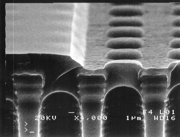
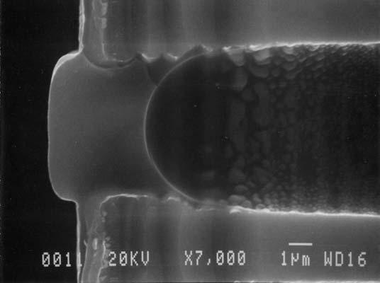
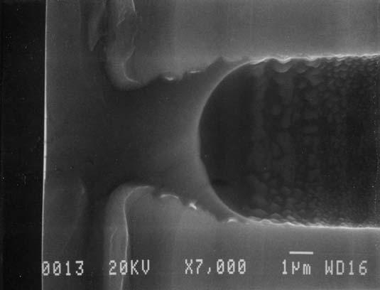
22 3-D photoresist definition Photoresist line
23 First results on MCz silicon at Irst rocess:. standard Irst process for detector realization 420 C). no LTO deposition (sintering at 380 C) Fz <111> n-type 6 Kohm MCz <100> n-type >0.5 Kohm FDV (V) > 1700 estimated Q ox (1/cm 2 ) 1.56E E E E V (na/cm 2 ) s 0 (cm/sec.)
irst: process development, characterization and first irradiation studies
 3D D detectors at ITC-irst irst: process development, characterization and first irradiation studies S. Ronchin a, M. Boscardin a, L. Bosisio b, V. Cindro c, G.-F. Dalla Betta d, C. Piemonte a, A. Pozza
Silicon Sensor Developments for the CMS Tracker Upgrade
 Silicon Sensor Developments for the CMS Tracker Upgrade on behalf of the CMS tracker collaboration University of Hamburg, Germany E-mail: Joachim.Erfle@desy.de CMS started a campaign to identify the future
Simulation and test of 3D silicon radiation detectors
 Simulation and test of 3D silicon radiation detectors C.Fleta 1, D. Pennicard 1, R. Bates 1, C. Parkes 1, G. Pellegrini 2, M. Lozano 2, V. Wright 3, M. Boscardin 4, G.-F. Dalla Betta 4, C. Piemonte 4,
SSD Development for the ATLAS Upgrade Tracker
 SSD Development for the ATLAS Upgrade Tracker Meeting Mo., Feb. 26, 2007. 2-6 pm; CERN Rm. 13-3-005 ATL-P-MN-0006 v.1 Development of non-inverting Silicon strip detectors for the ATLAS ID Upgrade 1) DC
A new Vertical JFET Technology for Harsh Radiation Applications
 A New Vertical JFET Technology for Harsh Radiation Applications ISPS 2016 1 A new Vertical JFET Technology for Harsh Radiation Applications A Rad-Hard switch for the ATLAS Inner Tracker P. Fernández-Martínez,
Radiation hardness and precision timing study of Silicon Detectors for the CMS High Granularity Calorimeter (HGC)
") Radiation hardness and precision timing study of Silicon Detectors for the CMS High Granularity Calorimeter (HGC) Esteban Currás1,2, Marcos Fernández2, Christian Gallrapp1, Marcello Mannelli1, Michael
Radiation hardness and precision timing study of Silicon Detectors for the CMS High Granularity Calorimeter (HGC) Esteban Currás1,2, Marcos Fernández2, Christian Gallrapp1, Marcello Mannelli1, Michael
Monolithic Pixel Sensors in SOI technology R&D activities at LBNL
 Monolithic Pixel Sensors in SOI technology R&D activities at LBNL Lawrence Berkeley National Laboratory M. Battaglia, L. Glesener (UC Berkeley & LBNL), D. Bisello, P. Giubilato (LBNL & INFN Padova), P.
The HGTD: A SOI Power Diode for Timing Detection Applications
 The HGTD: A SOI Power Diode for Timing Detection Applications Work done in the framework of RD50 Collaboration (CERN) M. Carulla, D. Flores, S. Hidalgo, D. Quirion, G. Pellegrini IMB-CNM (CSIC), Spain
Recent RD50 Developments on Radiation Tolerant Silicon Sensors
 4 th NoRHDia Workshop, GSI, Darmstadt, June 8-10, 2008 Recent RD50 Developments on Radiation Tolerant Silicon Sensors Michael Moll (CERN-PH PH-DT) OUTLINE Motivation, RD50, RD50 work program Radiation
Development of a large area silicon pad detector for the identification of cosmic ions
 Development of a large area silicon pad detector for the identification of cosmic ions M.Y. Kim 1,2 P.S. Marrocchesi 1, C. Avanzini 2, M.G. Bagliesi 1, G. Bigongiari 1,A. Caldarone 1,R. Cecchi 1,, P. Maestro
Measurements With Irradiated 3D Silicon Strip Detectors
 Measurements With Irradiated 3D Silicon Strip Detectors Michael Köhler, Michael Breindl, Karls Jakobs, Ulrich Parzefall, Liv Wiik University of Freiburg Celeste Fleta, Manuel Lozano, Giulio Pellegrini
PoS(EPS-HEP 2009)150. Silicon Detectors for the slhc - an Overview of Recent RD50 Results. Giulio Pellegrini 1. On behalf of CERN RD50 collaboration
150. Silicon Detectors for the slhc - an Overview of Recent RD50 Results. Giulio Pellegrini 1. On behalf of CERN RD50 collaboration") Silicon Detectors for the slhc - an Overview of Recent RD50 Results 1 Centro Nacional de Microelectronica CNM- IMB-CSIC, Barcelona Spain E-mail: giulio.pellegrini@imb-cnm.csic.es On behalf of CERN RD50
Silicon Detectors for the slhc - an Overview of Recent RD50 Results 1 Centro Nacional de Microelectronica CNM- IMB-CSIC, Barcelona Spain E-mail: giulio.pellegrini@imb-cnm.csic.es On behalf of CERN RD50
1. Reasons for using p-type SSD
 SCIPP 05/09 Operation of Short-Strip Silicon Detectors based on p-type Wafers in the ATLAS Upgrade ID Hartmut F.-W. Sadrozinski, Abraham Seiden SCIPP, UC Santa Cruz, CA 95064 Mara Bruzzi INFN Firenze -
Development of Radiation hard semiconductor devices for very high luminosity colliders
 Development of Radiation hard semiconductor devices for very high luminosity colliders Alberto Messineo University and INFN - Pisa WG-SLHC INFN-Frascati Nov 2005 Tracker upgrade : how to approach Integrated
Why p-type is better than n-type? or Electric field in heavily irradiated silicon detectors
 Why p-type is better than n-type? or Electric field in heavily irradiated silicon detectors G.Kramberger, V. Cindro, I. Mandić, M. Mikuž, M. Milovanović, M. Zavrtanik Jožef Stefan Institute Ljubljana,
Development of 3D detectors and
 Development of 3D detectors and SiPM @ ITC-irst Maurizio Boscardin boscardi@itc.it ITC-irst ITC (Istituto Trentino di Cultura) is a public research institute in Trento mainly funded by the local government
UNIVERSITY of CALIFORNIA SANTA CRUZ
 UNIVERSITY of CALIFORNIA SANTA CRUZ CHARACTERIZATION OF THE IRST PROTOTYPE P-TYPE SILICON STRIP SENSOR A thesis submitted in partial satisfaction of the requirements for the degree of BACHELOR OF SCIENCE
F. Hartmann. IEKP - Universität Karlsruhe (TH) IEKP - Universität Karlsruhe (TH)
 IEKP - Universität Karlsruhe (TH)") Results on proton irradiation tests in Karlsruhe p do Bulk & Surface Damage Strip parameters after irrad. V FD for (300µm) and 500µm sensors after 10 years LHC Expectedpower for500 µm sensors after 10
Results on proton irradiation tests in Karlsruhe p do Bulk & Surface Damage Strip parameters after irrad. V FD for (300µm) and 500µm sensors after 10 years LHC Expectedpower for500 µm sensors after 10
Silicon Sensor and Detector Developments for the CMS Tracker Upgrade
 Silicon Sensor and Detector Developments for the CMS Tracker Upgrade Università degli Studi di Firenze and INFN Sezione di Firenze E-mail: candi@fi.infn.it CMS has started a campaign to identify the future
Simulation of new P-type strip detectors with trench to enhance the charge multiplication effect in the n- type electrodes
 Simulation of new P-Type strip detectors RESMDD 10, Florence 12-15.October.2010 1/15 Simulation of new P-type strip detectors with trench to enhance the charge multiplication effect in the n- type electrodes
IRST SiPM characterizations and Application Studies
 IRST SiPM characterizations and Application Studies G. Pauletta for the FACTOR collaboration Outline 1. Introduction (who and where) 2. Objectives and program (what and how) 3. characterizations 4. Applications
AIDA-2020 Advanced European Infrastructures for Detectors at Accelerators. Milestone Report
 AIDA-2020-MS15 AIDA-2020 Advanced European Infrastructures for Detectors at Accelerators Milestone Report Design specifications of test stations for irradiated silicon sensors and LHC oriented front-end
SiPM development within the FBK/INFN collaboration. G. Ambrosi INFN Perugia
 SiPM development within the FBK/INFN collaboration G. Ambrosi INFN Perugia 2 FBK Trento (IT) Clean room «Detectors»: - 500m2-6 wafers - Equipped with: ion implanter 8 furnaces wet etching dry etching lithography
Silicon Sensors for HL LHC Tracking Detectors
 Silicon Sensors for HL LHC Tracking Detectors N25: Radiation Damage Effects 31. October 2012 Susanne Kuehn University of Freiburg, Germany On behalf of the RD50 Collaboration Outline Introduction Research
Development of Pixel Detectors for the Inner Tracker Upgrade of the ATLAS Experiment
 Development of Pixel Detectors for the Inner Tracker Upgrade of the ATLAS Experiment Natascha Savić L. Bergbreiter, J. Breuer, A. Macchiolo, R. Nisius, S. Terzo IMPRS, Munich # 29.5.215 Franz Dinkelacker
Silicon Sensors for High-Luminosity Trackers - RD50 Collaboration status report
 Silicon Sensors for High-Luminosity Trackers - RD50 Collaboration status report Albert-Ludwigs-Universität Freiburg (DE) E-mail: susanne.kuehn@cern.ch The revised schedule for the Large Hadron Collider
Signal-to. to-noise with SiGe. 7 th RD50 Workshop CERN. Hartmut F.-W. Sadrozinski. SCIPP UC Santa Cruz. Signal-to-Noise, SiGe 1
 Signal-to to-noise with SiGe 7 th RD50 Workshop CERN SCIPP UC Santa Cruz Signal-to-Noise, SiGe 1 Technical (Practical) Issues The ATLAS-ID upgrade will put large constraints on power. Can we meet power
ATLAS Upgrade SSD. ATLAS Upgrade SSD. Specifications of Electrical Measurements on SSD. Specifications of Electrical Measurements on SSD
 ATLAS Upgrade SSD Specifications of Electrical Measurements on SSD ATLAS Project Document No: Institute Document No. Created: 17/11/2006 Page: 1 of 7 DRAFT 2.0 Modified: Rev. No.: 2 ATLAS Upgrade SSD Specifications
The SIRAD irradiation facility at the INFN - Legnaro National Laboratory
 The SIRAD irradiation facility at the INFN - Legnaro National Laboratory I. Introduction 2 The INFN - Legnaro National Laboratory (LNL) SIRAD beamline http://www.lnl.infn.it 3 What is SIRAD? SIRAD is the
Single Sided and Double Sided Silicon MicroStrip Detector R&D
 Single Sided and Double Sided Silicon MicroStrip Detector R&D Tariq Aziz Tata Institute, Mumbai, India SuperBelle, KEK December 10-12, 2008 Indian Effort Mask Design at TIFR, Processing at BEL Single Sided
CMS Phase II Tracker Upgrade GRK-Workshop in Bad Liebenzell
 CMS Phase II Tracker Upgrade GRK-Workshop in Bad Liebenzell Institut für Experimentelle Kernphysik KIT University of the State of Baden-Wuerttemberg and National Research Center of the Helmholtz Association
Prototype Performance and Design of the ATLAS Pixel Sensor
 Prototype Performance and Design of the ATLAS Pixel Sensor F. Hügging, for the ATLAS Pixel Collaboration Contents: - Introduction - Sensor Concept - Performance fi before and after irradiation - Conclusion
CMS Tracker Upgrade for HL-LHC Sensors R&D. Hadi Behnamian, IPM On behalf of CMS Tracker Collaboration
 CMS Tracker Upgrade for HL-LHC Sensors R&D Hadi Behnamian, IPM On behalf of CMS Tracker Collaboration Outline HL-LHC Tracker Upgrade: Motivations and requirements Silicon strip R&D: * Materials with Multi-Geometric
Department of Physics & Astronomy
 Department of Physics & Astronomy Experimental Particle Physics Group Kelvin Building, University of Glasgow, Glasgow, G12 8QQ, Scotland Telephone: +44 (0)141 339 8855 Fax: +44 (0)141 330 5881 GLAS-PPE/2005-14
Simulation of High Resistivity (CMOS) Pixels
 Pixels") Simulation of High Resistivity (CMOS) Pixels Stefan Lauxtermann, Kadri Vural Sensor Creations Inc. AIDA-2020 CMOS Simulation Workshop May 13 th 2016 OUTLINE 1. Definition of High Resistivity Pixel Also
Simulation of High Resistivity (CMOS) Pixels Stefan Lauxtermann, Kadri Vural Sensor Creations Inc. AIDA-2020 CMOS Simulation Workshop May 13 th 2016 OUTLINE 1. Definition of High Resistivity Pixel Also
Forward bias operation of irradiated silicon detectors A.Chilingarov Lancaster University, UK
 1 st Workshop on Radiation hard semiconductor devices for very high luminosity colliders, CERN, 28-30 November 2001 Forward bias operation of irradiated silicon detectors A.Chilingarov Lancaster University,
Silicon Sensors for HL-LHC Tracking Detectors - RD50 Status Report
 Silicon Sensors for HL-LHC Tracking Detectors - RD50 Status Report Igor Mandić Jožef Stefan Institute, Ljubljana, Slovenia On behalf of RD50 collaboration RD50 Radiation hard semiconductor devices for
Studies of silicon strip sensors for the ATLAS ITK project. Miguel Arratia Cavendish Laboratory, University of Cambridge
 Studies of silicon strip sensors for the ATLAS ITK project Miguel Arratia Cavendish Laboratory, University of Cambridge 1 ITK project and radiation damage Unprecedented large fluences expected for the
Measurement results of DIPIX pixel sensor developed in SOI technology
 Measurement results of DIPIX pixel sensor developed in SOI technology Mohammed Imran Ahmed a,b, Yasuo Arai c, Marek Idzik a, Piotr Kapusta b, Toshinobu Miyoshi c, Micha l Turala b a AGH University of Science
Pixel detector development for the PANDA MVD
 Pixel detector development for the PANDA MVD D. Calvo INFN - Torino on behalf of the PANDA MVD group 532. WE-Heraeus-Seminar on Development of High_Resolution Pixel Detectors and their Use in Science and
SIM-Detecteurs 2014 LPNHE-Paris
 SIM-Detecteurs 2014 LPNHE-Paris The application of Silvaco process and device simulation program to the development of silicon detector for the high energy particle detection Li Long llong@cismst.de CiS
Lecture 020 ECE4430 Review II (1/5/04) Page 020-1
 Page 020-1") Lecture 020 ECE4430 Review II (1/5/04) Page 020-1 LECTURE 020 ECE 4430 REVIEW II (READING: GHLM - Chap. 2) Objective The objective of this presentation is: 1.) Identify the prerequisite material as taught
Lecture 020 ECE4430 Review II (1/5/04) Page 020-1 LECTURE 020 ECE 4430 REVIEW II (READING: GHLM - Chap. 2) Objective The objective of this presentation is: 1.) Identify the prerequisite material as taught
Cosmic Rays induced Single Event Effects in Power Semiconductor Devices
 Cosmic Rays induced Single Event Effects in Power Semiconductor Devices Giovanni Busatto University of Cassino ITALY Outline Introduction Cosmic rays in Space Cosmic rays at Sea Level Radiation Effects
PoS(Vertex 2016)028. Small pitch 3D devices. Gian-Franco Dalla Betta 1, Roberto Mendicino, DMS Sultan
028. Small pitch 3D devices. Gian-Franco Dalla Betta 1, Roberto Mendicino, DMS Sultan") 1, Roberto Mendicino, DMS Sultan University of Trento and TIFPA INFN Via Sommarive, 9 38123 Trento, Italy E-mail: gianfranco.dallabetta@unitn.it Maurizio Boscardin, Gabriele Giacomini 2, Sabina Ronchin,
1, Roberto Mendicino, DMS Sultan University of Trento and TIFPA INFN Via Sommarive, 9 38123 Trento, Italy E-mail: gianfranco.dallabetta@unitn.it Maurizio Boscardin, Gabriele Giacomini 2, Sabina Ronchin,
Development of Double-sided Silcon microstrip Detector. D.H. Kah*, H. Park, H.J. Kim (BAERI JikLee (SNU) E. Won (Korea U)
 E. Won (Korea U)") Development of Double-sided Silcon microstrip Detector D.H. Kah*, H. Park, H.J. Kim (BAERI JikLee (SNU) E. Won (Korea U), KNU) 2005 APPI dhkah@belle.knu.ac.kr 1 1. Motivation 2. Introduction Contents 1.
Development of Double-sided Silcon microstrip Detector D.H. Kah*, H. Park, H.J. Kim (BAERI JikLee (SNU) E. Won (Korea U), KNU) 2005 APPI dhkah@belle.knu.ac.kr 1 1. Motivation 2. Introduction Contents 1.
High-Ohmic Resistors using Nanometer-Thin Pure-Boron Chemical-Vapour-Deposited Layers
 High-Ohmic Resistors using Nanometer-Thin Pure-Boron Chemical-Vapour-Deposited Layers Negin Golshani, Vahid Mohammadi, Siva Ramesh, Lis K. Nanver Delft University of Technology The Netherlands ESSDERC
ATLAS Upgrade SSD Project:
 ATLAS Upgrade SSD: Specifications of the ATLAS Upgrade SSD ATLAS Project Document No: Institute Document No. Created: 30/10/2006 Page: 1 of 7 DRAFT 1.0 Modified: ATLAS Upgrade SSD Project: Specifications
Study of X-ray radiation damage in silicon sensors
 Journal of Instrumentation OPEN ACCESS Study of X-ray radiation damage in silicon sensors To cite this article: J Zhang et al View the article online for updates and enhancements. Recent citations - Demonstration
IV curves of different pixel cells
 IV curves of different pixel cells 6 5 100 µm pitch, 10µm gap 100 µm pitch, 50µm gap current [pa] 4 3 2 1 interface generation current volume generation current 0 0 50 100 150 200 250 bias voltage [V]
Evaluation of the Radiation Tolerance of Several Generations of SiGe Heterojunction Bipolar Transistors Under Radiation Exposure
 1 Evaluation of the Radiation Tolerance of Several Generations of SiGe Heterojunction Bipolar Transistors Under Radiation Exposure J. Metcalfe, D. E. Dorfan, A. A. Grillo, A. Jones, F. Martinez-McKinney,
AVALANCHE PHOTODIODES FOR THE CMS ELECTROMAGNETIC CALORIMETER
 AVALANCHE PHOTODIODES FOR THE CMS ELECTROMAGNETIC CALORIMETER B. Patel, R. Rusack, P. Vikas(email:Pratibha.Vikas@cern.ch) University of Minnesota, Minneapolis, U.S.A. Y. Musienko, S. Nicol, S.Reucroft,
Development of Integration-Type Silicon-On-Insulator Monolithic Pixel. Detectors by Using a Float Zone Silicon
 Development of Integration-Type Silicon-On-Insulator Monolithic Pixel Detectors by Using a Float Zone Silicon S. Mitsui a*, Y. Arai b, T. Miyoshi b, A. Takeda c a Venture Business Laboratory, Organization
Quality Assurance for the ATLAS Pixel Sensor
 Quality Assurance for the ATLAS Pixel Sensor 1st Workshop on Quality Assurance Issues in Silicon Detectors J. M. Klaiber-Lodewigs (Univ. Dortmund) for the ATLAS pixel collaboration Contents: - role of
arxiv: v2 [physics.ins-det] 15 Jan 2019
![arxiv: v2 [physics.ins-det] 15 Jan 2019](/thumbs/93/113829886.jpg "arxiv: v2 [physics.ins-det] 15 Jan 2019") Timing performance of small cell 3D silicon detectors arxiv:191.538v [physics.ins-det] 15 Jan 19 G. Kramberger a, V. Cindro a, D. Flores b, S. Hidalgo b, B. Hiti a, M. Manna b, I. Mandić a, M. Mikuž a,c,
Timing performance of small cell 3D silicon detectors arxiv:191.538v [physics.ins-det] 15 Jan 19 G. Kramberger a, V. Cindro a, D. Flores b, S. Hidalgo b, B. Hiti a, M. Manna b, I. Mandić a, M. Mikuž a,c,
Monolithic Pixel Detector in a 0.15µm SOI Technology
 Monolithic Pixel Detector in a 0.15µm SOI Technology 2006 IEEE Nuclear Science Symposium, San Diego, California, Nov. 1, 2006 Yasuo Arai (KEK) KEK Detector Technology Project : [SOIPIX Group] Y. Arai Y.
Sensor production readiness
 Sensor production readiness G. Bolla, Purdue University for the USCMS FPIX group PMG review 02/25/2005 2/23/2005 1 Outline Sensor requirements Geometry Radiation hardness Development Guard Rings P stops
Integrated diodes. The forward voltage drop only slightly depends on the forward current. ELEKTRONIKOS ĮTAISAI
 1 Integrated diodes pn junctions of transistor structures can be used as integrated diodes. The choice of the junction is limited by the considerations of switching speed and breakdown voltage. The forward
RD39 STATUS REPORT RD39 Collaboration
 EUROPEAN ORGANISATION FOR NUCLEAR RESEARCH CERN/LHCC 2000-010 06 January 2000 RD39 STATUS REPORT RD39 Collaboration K. Borer, S. Janos and K. Pretzl Laboratorium für Hochenergiephysik der Universität Bern,
The CMS Silicon Pixel Detector for HL-LHC
 * Institute for Experimental Physics Hamburg University Luruper Chaussee 149 22761 Hamburg, Germany E-mail: georg.steinbrueck@desy.de for the CMS collaboration The LHC is planning an upgrade program which
Silicon Detectors in High Energy Physics
 Thomas Bergauer (HEPHY Vienna) IPM Teheran 22 May 2011 Sunday: Schedule Semiconductor Basics (45 ) Silicon Detectors in Detector concepts: Pixels and Strips (45 ) Coffee Break Strip Detector Performance
Development of Ultra Fast Silicon Detectors for 4D Tracking
 Development of Ultra Fast Silicon Detectors for 4D Tracking V. Sola, R. Arcidiacono, R. Bellan, A. Bellora, S. Durando, N. Cartiglia, F. Cenna, M. Ferrero, V. Monaco, R. Mulargia, M.M. Obertino, R. Sacchi,
EE 5611 Introduction to Microelectronic Technologies Fall Thursday, September 04, 2014 Lecture 02
 EE 5611 Introduction to Microelectronic Technologies Fall 2014 Thursday, September 04, 2014 Lecture 02 1 Lecture Outline Review on semiconductor materials Review on microelectronic devices Example of microelectronic
IEEE TRANSACTIONS ON NUCLEAR SCIENCE, VOL. 55, NO. 5, OCTOBER /$ IEEE
 IEEE TRANSACTIONS ON NUCLEAR SCIENCE, VOL. 55, NO. 5, OCTOBER 2008 2775 Double-Sided, Double-Type-Column 3-D Detectors: Design, Fabrication, and Technology Evaluation Andrea Zoboli, Student Member, IEEE,
Topic 3. CMOS Fabrication Process
 Topic 3 CMOS Fabrication Process Peter Cheung Department of Electrical & Electronic Engineering Imperial College London URL: www.ee.ic.ac.uk/pcheung/ E-mail: p.cheung@ic.ac.uk Lecture 3-1 Layout of a Inverter
MOSFET & IC Basics - GATE Problems (Part - I)
") MOSFET & IC Basics - GATE Problems (Part - I) 1. Channel current is reduced on application of a more positive voltage to the GATE of the depletion mode n channel MOSFET. (True/False) [GATE 1994: 1 Mark]
MOSFET & IC Basics - GATE Problems (Part - I) 1. Channel current is reduced on application of a more positive voltage to the GATE of the depletion mode n channel MOSFET. (True/False) [GATE 1994: 1 Mark]
Silicon detectors for particle physics laboratory
 Silicon detectors for particle physics laboratory R. Bates 1, L. Eklund, N. Pacifico and M. Milovanovic 3 This laboratory would not have been possible without the financial help from the particle physics
New fabrication and packaging technologies for CMOS pixel sensors: closing gap between hybrid and monolithic
 New fabrication and packaging technologies for CMOS pixel sensors: closing gap between hybrid and monolithic Outline Short history of MAPS development at IPHC Results from TowerJazz CIS test sensor Ultra-thin
Julia Thom-Levy, Cornell University, for the CMS Collaboration. ECFA High Luminosity LHC Experiments Workshop-2016 October 3-6, 2016
 J.Thom-Levy October 5th, 2016 ECFA High Lumi LHC Experiments Pixel Detector R&D 1 Pixel Tracker R&D Cornell University Floyd R. Newman Laboratory for Elementary-Particle Physics Julia Thom-Levy, Cornell
Measurement of charge collec1on in irradiated miniature sensors for the upgrade of ATLAS Phase-II Strip tracker
 Measurement of charge collec1on in irradiated miniature sensors for the upgrade of ATLAS Phase-II Strip tracker Vladimir Cindro Jožef Stefan Institute, Ljubljana, Slovenia S.H. Abidi, A.A. Affolder, M.
TCAD simulations of silicon strip and pixel sensor optimization
 sensor optimization a, S. Mitsui a, S. Terada a, Y. Ikegami a, Y. Takubo a, K. Hara b, Y. Takahashi b, O. Jinnouchi c, T. Kishida c, R. Nagai c, S. Kamada d, and K. Yamamura d a KEK, Tsukuba b University
BaBar SVT: Radiation Damage and Other Operational Issues
 BaBar SVT: Radiation Damage and Other Operational Issues SLAC 1 Outline 2 Intro to BaBar and SVT Radiation Environment Damage to Si Detectors Damage to Front End Electronics Performance Degradation Other
EPE 2005 Dresden ESCAPEE. ESCAPEE Project. SiC Workshop. EPE 2005, September 12
 1 EPE 2005 Dresden ESCAPEE 2 The achievements of the EC funded project "Establish Silicon Carbide Applications for Power Electronics in Europe" (ESCAPEE) J. Millan 1, P. Godignon 1, D. Tournier 1, P.A.
Characteristics of the ALICE Silicon Drift Detector.
 Characteristics of the ALICE Silicon Drift Detector. A. Rashevsky b,1, V. Bonvicini b, P. Burger c, P. Cerello a, E. Crescio a, P. Giubellino a, R. Hernández-Montoya a,2, A. Kolojvari a,3, L.M. Montaño
 http://clicdp.cern.ch Hybrid Pixel Detectors with Active-Edge Sensors for the CLIC Vertex Detector Simon Spannagel on behalf of the CLICdp Collaboration Experimental Conditions at CLIC CLIC beam structure
Layout of a Inverter. Topic 3. CMOS Fabrication Process. The CMOS Process - photolithography (2) The CMOS Process - photolithography (1) v o.
 The CMOS Process - photolithography (1) v o.") Layout of a Inverter Topic 3 CMOS Fabrication Process V DD Q p Peter Cheung Department of Electrical & Electronic Engineering Imperial College London v i v o Q n URL: www.ee.ic.ac.uk/pcheung/ E-mail: p.cheung@ic.ac.uk
Layout of a Inverter Topic 3 CMOS Fabrication Process V DD Q p Peter Cheung Department of Electrical & Electronic Engineering Imperial College London v i v o Q n URL: www.ee.ic.ac.uk/pcheung/ E-mail: p.cheung@ic.ac.uk
Pixel sensors with different pitch layouts for ATLAS Phase-II upgrade
 Pixel sensors with different pitch layouts for ATLAS Phase-II upgrade Different pitch layouts are considered for the pixel detector being designed for the ATLAS upgraded tracking system which will be operating
The CMS Pixel Detector Upgrade and R&D Developments for the High Luminosity LHC
 The CMS Pixel Detector Upgrade and R&D Developments for the High Luminosity LHC On behalf of the CMS Collaboration INFN Florence (Italy) 11th 15th September 2017 Las Caldas, Asturias (Spain) High Luminosity
Thin Silicon R&D for LC applications
 Thin Silicon R&D for LC applications D. Bortoletto Purdue University Status report Hybrid Pixel Detectors for LC Next Linear Collider:Physic requirements Vertexing 10 µ mgev σ r φ,z(ip ) 5µ m 3 / 2 p sin
arxiv: v2 [physics.ins-det] 15 Feb 2013
![arxiv: v2 [physics.ins-det] 15 Feb 2013](/thumbs/91/105524489.jpg "arxiv: v2 [physics.ins-det] 15 Feb 2013") Novel Silicon n-on-p Edgeless Planar Pixel Sensors for the ATLAS upgrade arxiv:1212.3580v2 [physics.ins-det] 15 Feb 2013 1 2 3 4 5 6 7 8 9 10 11 12 13 14 15 16 17 18 M. Bomben a,, A. Bagolini b, M. Boscardin
Novel Silicon n-on-p Edgeless Planar Pixel Sensors for the ATLAS upgrade arxiv:1212.3580v2 [physics.ins-det] 15 Feb 2013 1 2 3 4 5 6 7 8 9 10 11 12 13 14 15 16 17 18 M. Bomben a,, A. Bagolini b, M. Boscardin
Ultra-Fast Silicon Detector
 Ultra-Fast Silicon Detector The 4D challenge A parameterization of time resolution The Low Gain Avalanche Detectors project Laboratory measurements UFSD: LGAD optimized for timing measurements WeightField2:
ECSE-6300 IC Fabrication Laboratory Lecture 9 MOSFETs. Lecture Outline
 ECSE-6300 IC Fabrication Laboratory Lecture 9 MOSFETs Prof. Rensselaer Polytechnic Institute Troy, NY 12180 Office: CII-6229 Tel.: (518) 276-2909 e-mails: luj@rpi.edu http://www.ecse.rpi.edu/courses/s18/ecse
FACTOR: first results on SiPM characterization
 FACTOR: first results on SiPM characterization Valter Bonvicini INFN Trieste OUTLINE: 1. Motivations and program of the FACTOR project 2. Types of devices tested, measurements performed and set-up used
CMS Beam Condition Monitoring Wim de Boer, Hannes Bol, Alexander Furgeri, Steffen Muller
 CMS Beam Condition Monitoring Wim de Boer, Hannes Bol, Alexander Furgeri, Steffen Muller BCM2 8diamonds BCM1 8diamonds each BCM2 8diamonds Beam Condition Monitoring at LHC BCM at LHC is done by about 3700
Review of Silicon Inner Tracker
 Review of Silicon Inner Tracker H.J.Kim (KyungPook National U.) Talk Outline Configuration optimization of BIT and FIT Silicon Sensor R&D Electronics R&D Summary and Plan Detail study will be presented
The BaBar Silicon Vertex Tracker (SVT) Claudio Campagnari University of California Santa Barbara
 Claudio Campagnari University of California Santa Barbara") The BaBar Silicon Vertex Tracker (SVT) Claudio Campagnari University of California Santa Barbara Outline Requirements Detector Description Performance Radiation SVT Design Requirements and Constraints
The BaBar Silicon Vertex Tracker (SVT) Claudio Campagnari University of California Santa Barbara Outline Requirements Detector Description Performance Radiation SVT Design Requirements and Constraints
A new Silicon Photomultiplier structure for blue light detection
 Nuclear Instruments and Methods in Physics Research A 568 (2006) 224 232 www.elsevier.com/locate/nima A new Silicon Photomultiplier structure for blue light detection Claudio Piemonte ITC-irst, Divisione
Recent Technological Developments on LGAD and ilgad Detectors for Tracking and Timing Applications
 Recent Technological Developments on LGAD and ilgad Detectors for Tracking and Timing Applications G. Pellegrini 1, M. Baselga 1, M. Carulla 1, V. Fadeyev 2, P. Fernández-Martínez 1, M. Fernández García
AIDA Advanced European Infrastructures for Detectors at Accelerators. Journal Publication
 AIDA-PUB-13- AIDA Advanced European Infrastructures for Detectors at Accelerators Journal Publication Thin n-in-p pixel sensors and the SLID-ICV vertical integration technology for the ATLAS upgrade at
TRINAT Amplifier-Shaper for Silicon Detector (TASS)
") Sept. 8, 20 L. Kurchaninov TRINAT Amplifier-Shaper for Silicon Detector (TASS). General description Preamplifier-shaper for TRINAT Si detector (Micron model BB) is charge-sensitive amplifier followed by
Sept. 8, 20 L. Kurchaninov TRINAT Amplifier-Shaper for Silicon Detector (TASS). General description Preamplifier-shaper for TRINAT Si detector (Micron model BB) is charge-sensitive amplifier followed by
Fabrication, Corner, Layout, Matching, & etc.
 Advanced Analog Building Blocks Fabrication, Corner, Layout, Matching, & etc. Wei SHEN (KIP) 1 Fabrication Steps for MOS Wei SHEN, Universität Heidelberg 2 Fabrication Steps for MOS Wei SHEN, Universität
The CMS Silicon Strip Tracker and its Electronic Readout
 The CMS Silicon Strip Tracker and its Electronic Readout Markus Friedl Dissertation May 2001 M. Friedl The CMS Silicon Strip Tracker and its Electronic Readout 2 Introduction LHC Large Hadron Collider:
A Prototype Amplifier-Discriminator Chip for the GLAST Silicon-Strip Tracker
 A Prototype Amplifier-Discriminator Chip for the GLAST Silicon-Strip Tracker Robert P. Johnson Pavel Poplevin Hartmut Sadrozinski Ned Spencer Santa Cruz Institute for Particle Physics The GLAST Project
Maxim MAX3940E Electro-Absorption Modulator Structural Analysis
 May 23, 2006 Maxim MAX3940E Electro-Absorption Modulator Structural Analysis For comments, questions, or more information about this report, or for any additional technical needs concerning semiconductor
Monitoring of the Fabrication Process of Silicon Strip Sensors for Large Scale Productions
 SNIC Symposium, Stanford, California -- 3-6 April 26 Monitoring of the Fabrication Process of Silicon Strip Sensors for Large Scale Productions T. Bergauer Institute for High Energy Physics of the Austrian
SDD from device modeling to mass production - practical experience
 SDD from device modeling to mass production - practical experience Outline Motivations ALICE at LHC ITS&SDD system From specs to detector HV divider & stability Injectors & speed variations NTD fluctuations
ORTEC. Research Applications. Pulse-Height, Charge, or Energy Spectroscopy. Detectors. Processing Electronics
 ORTEC Spectroscopy systems for ORTEC instrumentation produce pulse height distributions of gamma ray or alpha energies. MAESTRO-32 (model A65-B32) is the software included with most spectroscopy systems
21 rue La Noue Bras de Fer Nantes - France Phone : +33 (0) w7-foldite :
 w7-foldite :") 21 rue La Noue Bras de Fer 44200 - Nantes - France Phone : +33 (0) 240 180 916 - email : info@systemplus.fr - w7-foldite : www.systemplus.fr February 2013 Version 1 Written by: Sylvain HALLEREAU DISCLAIMER
21 rue La Noue Bras de Fer 44200 - Nantes - France Phone : +33 (0) 240 180 916 - email : info@systemplus.fr - w7-foldite : www.systemplus.fr February 2013 Version 1 Written by: Sylvain HALLEREAU DISCLAIMER
RD53 status and plans
 RD53 status and plans Luigi Gaioni a,b On behalf of the RD53 Collaboration a University of Bergamo b INFN Pavia The 25 th International Workshop on Vertex Detectors VERTEX 2016 25-30 September 2016 - La
Role of guard rings in improving the performance of silicon detectors
 PRAMANA c Indian Academy of Sciences Vol. 65, No. 2 journal of August 2005 physics pp. 259 272 Role of guard rings in improving the performance of silicon detectors VIJAY MISHRA, V D SRIVASTAVA and S K