SiPM development within the FBK/INFN collaboration. G. Ambrosi INFN Perugia
|
|
|
- Damon Miller
- 6 years ago
- Views:
Transcription
1 SiPM development within the FBK/INFN collaboration G. Ambrosi INFN Perugia


2 2 FBK Trento (IT) Clean room «Detectors»: - 500m2-6 wafers - Equipped with: ion implanter 8 furnaces wet etching dry etching lithography stepper mask aligner Deep RIE Plasma-enhanced CVD sputtering


3 3 SiPM Characterization 1. IV measurement 3. Optical characterization 2. Dark characterization 4. Functional charact.

4 4 Dark measurement We acquire ms-long waveforms Signal filtered to reduce its length Procedure developed and implemented by FBK time delay array amplitude array
5 5 Dark measurement primary dark rate (DCR) direct cross-talk delayed correlated components measurements performed in FBK
6 6 Important features (at the system level) Breakdown voltage uniformity Temperature stability Packaging type (dead border region, TSV, custom package) COST: solutions to improve performance must be cost-effective.
 new junction excellent breakdown voltage uniformity low breakdown")
 electric field engineering excellent breakdown voltage uniformity low")

7 FBK technology evolution Original technology RGB-SiPM (Red-Green-Blue SiPM) 2012 NUV-SiPM (Near-UV SiPM) new junction excellent breakdown voltage uniformity low breakdown voltage temperature dependence 2012 higher efficiency lower noise RGB-SiPM_HD (Red-Green-Blue SiPM high density) electric field engineering excellent breakdown voltage uniformity low breakdown voltage temperature dependence high efficiency in the near-ultraviolet very low dark noise 7 small cell size with high fill factor: - high dynamic range - low excess noise factor new cell border
8 8 RGB Re-design of the active area: electric field engineer. Lower electric field, thicker high-field region + partially depleted epi at breakdown voltage Next slide: comparison between two SiPMs 1x1mm2 50x50um2 having exactly the same layout (FF ~45%). N.Serra: «Characterization of new FBK SiPM technology for visible light detection, JINST 2013 JINST 8 P03019

9 9 RGB: breakdown voltage breakdown voltage non-uniformity strongly reduced both at wafer level and from wafer to wafer FBK measurements breakdown voltage and DCR temperature dependence
10 10 RGB: photo-detection efficinecy PDE vs wavelength RGB PDE vs over-voltage 560nm 400nm original RGB: Much faster increase of efficiency vs over-voltage. As in original, peak is at green, consistent with junction type measurements performed in FBK
11 11 NUV SiPM Same electric field configuration of RGB technology but with opposite sign. Objective: maintain the advantages of RGB but with peak efficiency in the near-uv For more details, see: IEEE TRANSACTIONS ON NUCLEAR SCIENCE, VOL. 60, NO. 3, JUNE 2013
12 Breakdown voltage Breakdown voltage uniformity on a wafer. Temperature dependence of the breakdown voltage. measurements performed in FBK 12
13 Gain and noise Gain of 50x50 and 25x25um 2 cells. Gain pulse: extracted from area of single cell signal Gain current: extracted from ratio between DC current and primary dark rate NUV-SiPM: 1x1mm 2 50x50um 2. Total and primary dark count rate at 0.5 p.e. FBK measurements 13
14 Photo-detection efficiency PDE vs wavelength for a NUV-SiPM and RGB-SiPM with 50x50um 2 cell, 42% fill factor. PDE@380nm vs Overvoltage for a NUV-SiPM and RGB-SiPM with 50x50um 2 cell, 42% fill factor. FBK measurements 14
15 15 NUV vs RGB Original n+/ p RGB-SiPM (Upgraded n+/p) HD NUV-SiPM Breakdown voltage 33V 28V 28 26V Breakdown voltage uniformity on wafer ~3V <0.2V <0.2V <0.2V Max over-voltage ~8V ~6V ~8V ~5V V BD temp. coeff. 75mV/C 25mV/C 25mV/C 25mV/C Max primary dark rate (20C) several MHz/ mm 2 ~500kHz/mm 2 ~2MHz/mm 2 ~150kHz/mm 2 Peak PDE nm nm nm 390nm Wavelength range Peak PDE 25% 33% 30% 32% ECF (at max PDE) um cell 45% FF 15um cell 45% FF
16 16 What s next? FBK: further development of the SiPM small cell (15-20 µm) and high FF Functional devices have been produced with the stepper obtaining a fill factor of 65% good, but also the ECF is much higher!! optimize optical properties INFN: definition of custom geometries based on ~ 12x12 mm 2 single device: - monolitich array of 16 elements, 3x3 mm2 - monolitich array of 4elements, 6x6 mm2 - exagonal devices - custom assembly and packaging standard devices (3x3 mm 2, 4x4 mm 2 ) available fall 2013, new devices available in January 2014

17 17


18 large surface array 8x8 single SiPMs 1.5 mm pitch 1.2 x 1.2 cm2

19 19 Correlated noise Some paths for optical cross-talk - Trenches to avoid direct and delayed cross-talk - buried junction to avoid out-diffusion - lower gain!
20 RGB-HD (FBK design) FBK completely re-designed the cell border structure of RGB tech. to have small cells with high fill factor, L = 2um. In the previous technology it was 6/7um 20
arxiv: v1 [astro-ph.im] 19 Nov 2014
![arxiv: v1 [astro-ph.im] 19 Nov 2014](/thumbs/72/66682521.jpg "arxiv: v1 [astro-ph.im] 19 Nov 2014") Measurements and tests on FBK silicon sensors with an optimized electronic design for a CTA camera arxiv:1411.5241v1 [astro-ph.im] 19 Nov 214 G. Ambrosi (1), M. Ambrosio (2), C. Aramo (2), E. Bissaldi
Measurements and tests on FBK silicon sensors with an optimized electronic design for a CTA camera arxiv:1411.5241v1 [astro-ph.im] 19 Nov 214 G. Ambrosi (1), M. Ambrosio (2), C. Aramo (2), E. Bissaldi
IRST SiPM characterizations and Application Studies
 IRST SiPM characterizations and Application Studies G. Pauletta for the FACTOR collaboration Outline 1. Introduction (who and where) 2. Objectives and program (what and how) 3. characterizations 4. Applications
Near Ultraviolet (NUV) SiPMs
 SiPMs") Silicon photomultipliers (SiPMs) from First Sensor are innovative solid-state silicon detectors with single photon sensitivity. SiPMs are a valid alternative to photomultiplier tubes. The main benefits
Silicon photomultipliers (SiPMs) from First Sensor are innovative solid-state silicon detectors with single photon sensitivity. SiPMs are a valid alternative to photomultiplier tubes. The main benefits
AFBR-S4N44C013-DS100. Data Sheet. NUV-HD Silicon Photo Multiplier. Features. Description. Applications
 Data Sheet AFBR-S4N44C013 Description The AFBR-S4N44C013 is a silicon photo multiplier (SiPM) used for ultra-sensitive precision measurement of single photons. The active area is 3.72 x 3.72 mm 2. High
Introduction to silicon photomultipliers (SiPMs) White paper
 White paper") Introduction to silicon photomultipliers (SiPMs) White paper Basic structure and operation The silicon photomultiplier (SiPM) is a radiation detector with extremely high sensitivity, high efficiency, and
Introduction to silicon photomultipliers (SiPMs) White paper Basic structure and operation The silicon photomultiplier (SiPM) is a radiation detector with extremely high sensitivity, high efficiency, and
AFBR-S4N44P163-DS102. Data Sheet. 4 4 NUV-HD Silicon Photo Multiplier Array. Description. Features. Applications
 Data Sheet FBR-S4N44P163 Description The FBR-S4N44P163 is a 4 4 Silicon Photo Multiplier (SiPM) array used for ultra-sensitive precision measurements of single photons. The pitch of SiPMs is 4 mm in both
Red, Green, Blue (RGB) SiPMs
 SiPMs") Silicon photomultipliers (SiPMs) from First Sensor are innovative solid-state silicon detectors with single photon sensitivity. SiPMs are a valid alternative to photomultiplier tubes. The main benefits
Silicon photomultipliers (SiPMs) from First Sensor are innovative solid-state silicon detectors with single photon sensitivity. SiPMs are a valid alternative to photomultiplier tubes. The main benefits
CMOS 0.18 m SPAD. TowerJazz February, 2018 Dr. Amos Fenigstein
 CMOS 0.18 m SPAD TowerJazz February, 2018 Dr. Amos Fenigstein Outline CMOS SPAD motivation Two ended vs. Single Ended SPAD (bulk isolated) P+/N two ended SPAD and its optimization Application of P+/N two
FBK SiPM test with a charge integration FE
 FBK SiPM test with a charge integration FE F.Giordano 1, E.Bissaldi 2, M. Cilmo 3, G.Pastore 4, R.Rando 5 1 INFN Bari, 2 INFN Trieste, 3 INFN Napoli, 4 INFN Pisa, 5 INFN Padova For the CTA INFN R&D Project
Review of Solidstate Photomultiplier. Developments by CPTA & Photonique SA
 Review of Solidstate Photomultiplier Developments by CPTA & Photonique SA Victor Golovin Center for Prospective Technologies & Apparatus (CPTA) & David McNally - Photonique SA 1 Overview CPTA & Photonique
State of the art and perspectives of CMOS avalanche detectors
 State of the art and perspectives of CMOS avalanche detectors Lucio Pancheri DII, University of Trento & TIFPA-INFN, Italy CERN seminar January 20, 2017 Research on silicon detectors in Trento FBK Clean
Low Dark Count UV-SiPM: Development and Performance Measurements P. Bérard, M. Couture, P. Deschamps, F. Laforce H. Dautet and A.
 Low Dark Count UV-SiPM: Development and Performance Measurements P. Bérard, M. Couture, P. Deschamps, F. Laforce H. Dautet and A. Barlow LIGHT 11 Workshop on the Latest Developments of Photon Detectors
SiPM Module PRELIMINARY
 The integrates a stable voltage supply, signal amplification, interfaces and the SiPM detector in a compact plug and play unit. Included software allows optimization of the operating point of the detector
Characterization of SiPMs for Large Scale Applications
 SiPM KETEK SiPM Characterization of SiPMs for Large Scale Applications Eugen Engelmann (eugen.engelmann@ketek.net) 1 SiPM KETEK Family-owned enterprise, founded in 1989 by Dr. Josef Kemmer Number of employees:
Status of ITC-irst activities in RD50
 Status of ITC-irst activities in RD50 M. Boscardin ITC-irst, Microsystem Division Trento, Italy Outline Materials/Pad Detctors Pre-irradiated silicon INFN Padova and Institute for Nuclear Research of NASU,
J-Series High PDE and Timing Resolution, TSV Package
 High PDE and Timing Resolution SiPM Sensors in a TSV Package SensL s J-Series low-light sensors feature a high PDE (photon detection efficiency) that is achieved using a high-volume, P-on-N silicon foundry
Characterization of a prototype matrix of Silicon PhotoMultipliers (SiPM s)
") Characterization of a prototype matrix of Silicon PhotoMultipliers (SiPM s) N. Dinu, P. Barrillon, C. Bazin, S. Bondil-Blin, V. Chaumat, C. de La Taille, V. Puill, JF. Vagnucci Laboratory of Linear Accelerator
Characterization of a prototype matrix of Silicon PhotoMultipliers (SiPM s) N. Dinu, P. Barrillon, C. Bazin, S. Bondil-Blin, V. Chaumat, C. de La Taille, V. Puill, JF. Vagnucci Laboratory of Linear Accelerator
450mm patterning out of darkness Backend Process Exposure Tool SOKUDO Lithography Breakfast Forum July 10, 2013 Doug Shelton Canon USA Inc.
 450mm patterning out of darkness Backend Process Exposure Tool SOKUDO Lithography Breakfast Forum 2013 July 10, 2013 Doug Shelton Canon USA Inc. Introduction Half Pitch [nm] 2013 2014 2015 2016 2017 2018
Lecture 7. Lithography and Pattern Transfer. Reading: Chapter 7
 Lecture 7 Lithography and Pattern Transfer Reading: Chapter 7 Used for Pattern transfer into oxides, metals, semiconductors. 3 types of Photoresists (PR): Lithography and Photoresists 1.) Positive: PR
ECSE-6300 IC Fabrication Laboratory Lecture 9 MOSFETs. Lecture Outline
 ECSE-6300 IC Fabrication Laboratory Lecture 9 MOSFETs Prof. Rensselaer Polytechnic Institute Troy, NY 12180 Office: CII-6229 Tel.: (518) 276-2909 e-mails: luj@rpi.edu http://www.ecse.rpi.edu/courses/s18/ecse
ECSE-6300 IC Fabrication Laboratory Lecture 7 MOSFETs. Lecture Outline
 ECSE-6300 IC Fabrication Laboratory Lecture 7 MOSFETs Prof. Rensselaer Polytechnic Institute Troy, NY 12180 Office: CII-6229 Tel.: (518) 276-2909 e-mails: luj@rpi.edu http://www.ecse.rpi.edu/courses/s16/ecse
Major Fabrication Steps in MOS Process Flow
 Major Fabrication Steps in MOS Process Flow UV light Mask oxygen Silicon dioxide photoresist exposed photoresist oxide Silicon substrate Oxidation (Field oxide) Photoresist Coating Mask-Wafer Alignment
Geiger-mode APDs (2)
") (2) Masashi Yokoyama Department of Physics, University of Tokyo Nov.30-Dec.4, 2009, INFN/LNF Plan for today 1. Basic performance (cont.) Dark noise, cross-talk, afterpulsing 2. Radiation damage 2 Parameters
(2) Masashi Yokoyama Department of Physics, University of Tokyo Nov.30-Dec.4, 2009, INFN/LNF Plan for today 1. Basic performance (cont.) Dark noise, cross-talk, afterpulsing 2. Radiation damage 2 Parameters
SILICON PHOTOMULTIPLIERS: FROM 0 TO IN 1 NANOSECOND. Giovanni Ludovico Montagnani polimi.it
 SILICON PHOTOMULTIPLIERS: FROM 0 TO 10000 IN 1 NANOSECOND Giovanni Ludovico Montagnani Giovanniludovico.montagnani@ polimi.it LESSON OVERVIEW 1. Motivations: why SiPM are useful 2. SiPM applications examples
Single-Photon Time-of-Flight Sensors for Spacecraft Navigation and Landing in CMOS Technologies
 Single-Photon Time-of-Flight Sensors for Spacecraft Navigation and Landing in CMOS Technologies David Stoppa Fondazione Bruno Kessler, Trento, Italy Section V.C: Electronic Nanodevices and Technology Trends
The HGTD: A SOI Power Diode for Timing Detection Applications
 The HGTD: A SOI Power Diode for Timing Detection Applications Work done in the framework of RD50 Collaboration (CERN) M. Carulla, D. Flores, S. Hidalgo, D. Quirion, G. Pellegrini IMB-CNM (CSIC), Spain
Silicon Carbide Solid-State Photomultiplier for UV Light Detection
 Silicon Carbide Solid-State Photomultiplier for UV Light Detection Sergei Dolinsky, Stanislav Soloviev, Peter Sandvik, and Sabarni Palit GE Global Research 1 Why Solid-State? PMTs are sensitive to magnetic
Jan Bogaerts imec
 imec 2007 1 Radiometric Performance Enhancement of APS 3 rd Microelectronic Presentation Days, Estec, March 7-8, 2007 Outline Introduction Backside illuminated APS detector Approach CMOS APS (readout)
Semiconductor Manufacturing Technology. Semiconductor Manufacturing Technology. Photolithography: Resist Development and Advanced Lithography
 Semiconductor Manufacturing Technology Michael Quirk & Julian Serda October 2001 by Prentice Hall Chapter 15 Photolithography: Resist Development and Advanced Lithography Eight Basic Steps of Photolithography
Monolithic Pixel Sensors in SOI technology R&D activities at LBNL
 Monolithic Pixel Sensors in SOI technology R&D activities at LBNL Lawrence Berkeley National Laboratory M. Battaglia, L. Glesener (UC Berkeley & LBNL), D. Bisello, P. Giubilato (LBNL & INFN Padova), P.
Silicon Photomultiplier
 Silicon Photomultiplier Operation, Performance & Possible Applications Slawomir Piatek Technical Consultant, Hamamatsu Corp. Introduction Very high intrinsic gain together with minimal excess noise make
How to Evaluate and Compare Silicon Photomultiplier Sensors. October 2015
 The Silicon Photomultiplier (SiPM) is a single-photon sensitive light sensor that combines performance characteristics that exceed those of a PMT, with the practical advantages of a solid state sensor.
Nuclear Instruments and Methods in Physics Research A
 Nuclear Instruments and Methods in Physics Research A ] (]]]]) ]]] ]]] Contents lists available at SciVerse ScienceDirect Nuclear Instruments and Methods in Physics Research A journal homepage: www.elsevier.com/locate/nima
CMOS Digital Integrated Circuits Lec 2 Fabrication of MOSFETs
 CMOS Digital Integrated Circuits Lec 2 Fabrication of MOSFETs 1 CMOS Digital Integrated Circuits 3 rd Edition Categories of Materials Materials can be categorized into three main groups regarding their
SINPHOS SINGLE PHOTON SPECTROMETER FOR BIOMEDICAL APPLICATION
 -LNS SINPHOS SINGLE PHOTON SPECTROMETER FOR BIOMEDICAL APPLICATION Salvatore Tudisco 9th Topical Seminar on Innovative Particle and Radiation Detectors 23-26 May 2004 Siena, Italy Delayed Luminescence
Section 2: Lithography. Jaeger Chapter 2 Litho Reader. EE143 Ali Javey Slide 5-1
 Section 2: Lithography Jaeger Chapter 2 Litho Reader EE143 Ali Javey Slide 5-1 The lithographic process EE143 Ali Javey Slide 5-2 Photolithographic Process (a) (b) (c) (d) (e) (f) (g) Substrate covered
Lecture: Integration of silicon photonics with electronics. Prepared by Jean-Marc FEDELI CEA-LETI
 Lecture: Integration of silicon photonics with electronics Prepared by Jean-Marc FEDELI CEA-LETI Context The goal is to give optical functionalities to electronics integrated circuit (EIC) The objectives
R. Rando Daniele Corti, Christian Manea, Mosè Mariotti, Cornelia Schultz. INFN-Padova Report. Outline:
 R. Rando Daniele Corti, Christian Manea, Mosè Mariotti, Cornelia Schultz INFN-Padova Report Outline: Electronics (SiPM sum, no preamp) Optics (lenses etc) 1 Electronics 2 Old electronics (last meeting)
Section 2: Lithography. Jaeger Chapter 2. EE143 Ali Javey Slide 5-1
 Section 2: Lithography Jaeger Chapter 2 EE143 Ali Javey Slide 5-1 The lithographic process EE143 Ali Javey Slide 5-2 Photolithographic Process (a) (b) (c) (d) (e) (f) (g) Substrate covered with silicon
FUTURE PROSPECTS FOR CMOS ACTIVE PIXEL SENSORS
 FUTURE PROSPECTS FOR CMOS ACTIVE PIXEL SENSORS Dr. Eric R. Fossum Jet Propulsion Laboratory Dr. Philip H-S. Wong IBM Research 1995 IEEE Workshop on CCDs and Advanced Image Sensors April 21, 1995 CMOS APS
Development of 3D detectors and
 Development of 3D detectors and SiPM @ ITC-irst Maurizio Boscardin boscardi@itc.it ITC-irst ITC (Istituto Trentino di Cultura) is a public research institute in Trento mainly funded by the local government
EE 143 Microfabrication Technology Fall 2014
 EE 143 Microfabrication Technology Fall 2014 Prof. Clark T.-C. Nguyen Dept. of Electrical Engineering & Computer Sciences University of California at Berkeley Berkeley, CA 94720 EE 143: Microfabrication
PoS(PhotoDet 2012)058
058") Absolute Photo Detection Efficiency measurement of Silicon PhotoMultipliers Vincent CHAUMAT 1, Cyril Bazin, Nicoleta Dinu, Véronique PUILL 1, Jean-François Vagnucci Laboratoire de l accélérateur Linéaire,
Absolute Photo Detection Efficiency measurement of Silicon PhotoMultipliers Vincent CHAUMAT 1, Cyril Bazin, Nicoleta Dinu, Véronique PUILL 1, Jean-François Vagnucci Laboratoire de l accélérateur Linéaire,
Thermal and electrical characterization of silicon photomultiplier
 University of Wollongong Research Online Faculty of Engineering and Information Sciences - Papers: Part A Faculty of Engineering and Information Sciences 2008 Thermal and electrical characterization of
Part 5-1: Lithography
 Part 5-1: Lithography Yao-Joe Yang 1 Pattern Transfer (Patterning) Types of lithography systems: Optical X-ray electron beam writer (non-traditional, no masks) Two-dimensional pattern transfer: limited
Production of HPDs for the LHCb RICH Detectors
 Production of HPDs for the LHCb RICH Detectors LHCb RICH Detectors Hybrid Photon Detector Production Photo Detector Test Facilities Test Results Conclusions IEEE Nuclear Science Symposium Wyndham, 24 th
Recent Development and Study of Silicon Solid State Photomultiplier (MRS Avalanche Photodetector)
") Recent Development and Study of Silicon Solid State Photomultiplier (MRS Avalanche Photodetector) Valeri Saveliev University of Obninsk, Russia Vienna Conference on Instrumentation Vienna, 20 February
Recent Development and Study of Silicon Solid State Photomultiplier (MRS Avalanche Photodetector) Valeri Saveliev University of Obninsk, Russia Vienna Conference on Instrumentation Vienna, 20 February
Innovative Mask Aligner Lithography for MEMS and Packaging
 Innovative Mask Aligner Lithography for MEMS and Packaging Dr. Reinhard Voelkel CEO SUSS MicroOptics SA September 9 th, 2010 1 SUSS Micro-Optics SUSS MicroOptics is a leading supplier for high-quality
Characteristics of a prototype matrix of Silicon PhotoMultipliers (SiPM)
") Journal of Instrumentation OPEN ACCESS Characteristics of a prototype matrix of Silicon PhotoMultipliers (SiPM) To cite this article: N Dinu et al View the article online for updates and enhancements.
Journal of Instrumentation OPEN ACCESS Characteristics of a prototype matrix of Silicon PhotoMultipliers (SiPM) To cite this article: N Dinu et al View the article online for updates and enhancements.
Lecture 5. Optical Lithography
 Lecture 5 Optical Lithography Intro For most of microfabrication purposes the process (e.g. additive, subtractive or implantation) has to be applied selectively to particular areas of the wafer: patterning
Section 2: Lithography. Jaeger Chapter 2 Litho Reader. The lithographic process
 Section 2: Lithography Jaeger Chapter 2 Litho Reader The lithographic process Photolithographic Process (a) (b) (c) (d) (e) (f) (g) Substrate covered with silicon dioxide barrier layer Positive photoresist
Development of a LFLE Double Pattern Process for TE Mode Photonic Devices. Mycahya Eggleston Advisor: Dr. Stephen Preble
 Development of a LFLE Double Pattern Process for TE Mode Photonic Devices Mycahya Eggleston Advisor: Dr. Stephen Preble 2 Introduction and Motivation Silicon Photonics Geometry, TE vs TM, Double Pattern
Vertical Nanowall Array Covered Silicon Solar Cells
 International Conference on Solid-State and Integrated Circuit (ICSIC ) IPCSIT vol. () () IACSIT Press, Singapore Vertical Nanowall Array Covered Silicon Solar Cells J. Wang, N. Singh, G. Q. Lo, and D.
CHAPTER 2 POLARIZATION SPLITTER- ROTATOR BASED ON A DOUBLE- ETCHED DIRECTIONAL COUPLER
 CHAPTER 2 POLARIZATION SPLITTER- ROTATOR BASED ON A DOUBLE- ETCHED DIRECTIONAL COUPLER As we discussed in chapter 1, silicon photonics has received much attention in the last decade. The main reason is
FACTOR: first results on SiPM characterization
 FACTOR: first results on SiPM characterization Valter Bonvicini INFN Trieste OUTLINE: 1. Motivations and program of the FACTOR project 2. Types of devices tested, measurements performed and set-up used
Simulation and test of 3D silicon radiation detectors
 Simulation and test of 3D silicon radiation detectors C.Fleta 1, D. Pennicard 1, R. Bates 1, C. Parkes 1, G. Pellegrini 2, M. Lozano 2, V. Wright 3, M. Boscardin 4, G.-F. Dalla Betta 4, C. Piemonte 4,
Design Rules for Silicon Photonics Prototyping
 Design Rules for licon Photonics Prototyping Version 1 (released February 2008) Introduction IME s Photonics Prototyping Service offers 248nm lithography based fabrication technology for passive licon-on-insulator
FOUNDRY SERVICE. SEI's FEATURE. Wireless Devices FOUNDRY SERVICE. SRD-800DD, SRD-500DD D-FET Process Lg=0.8, 0.5µm. Ion Implanted MESFETs SRD-301ED
 FOUNDRY SERVICE 01.04. Foundry services have been one of the core businesses at SEI, providing sophisticated GaAs IC technology for all customers. SEI offers very flexible service to support the customers
A New Single-Photon Avalanche Diode in 90nm Standard CMOS Technology
 A New Single-Photon Avalanche Diode in 90nm Standard CMOS Technology Mohammad Azim Karami* a, Marek Gersbach, Edoardo Charbon a a Dept. of Electrical engineering, Technical University of Delft, Delft,
A tracking detector to study O(1 GeV) ν μ CC interactions
 ν μ CC interactions") A tracking detector to study O(1 GeV) ν μ CC interactions Laura Pasqualini on behalf of the mm-tracker Collaboration IPRD16, 3-6 October 2016, Siena Motivations ν/μ Tracking system for a light magnetic
A tracking detector to study O(1 GeV) ν μ CC interactions Laura Pasqualini on behalf of the mm-tracker Collaboration IPRD16, 3-6 October 2016, Siena Motivations ν/μ Tracking system for a light magnetic
Low On-Resistance Trench Lateral Power MOS Technology
 Low On-Resistance Trench Lateral Power MO Technology Akio ugi Mutsumi awada Naoto Fujishima 1. Introduction Market demands for smaller sized, lighter weight, lower power consuming and higher efficiency
Diode Sensor Lab. Dr. Lynn Fuller
 ROCHESTER INSTITUTE OF TECHNOLOGY MICROELECTRONIC ENGINEERING Diode Sensor Lab Dr. Lynn Fuller Webpage: http://people.rit.edu/lffeee 82 Lomb Memorial Drive Rochester, NY 14623-5604 Tel (585) 475-2035 Fax
EE C245 / ME C218 INTRODUCTION TO MEMS DESIGN FALL 2011 PROBLEM SET #2. Due (at 7 p.m.): Tuesday, Sept. 27, 2011, in the EE C245 HW box in 240 Cory.
: Tuesday, Sept. 27, 2011, in the EE C245 HW box in 240 Cory.") Issued: Tuesday, Sept. 13, 2011 PROBLEM SET #2 Due (at 7 p.m.): Tuesday, Sept. 27, 2011, in the EE C245 HW box in 240 Cory. 1. Below in Figure 1.1 is a description of a DRIE silicon etch using the Marvell
Issued: Tuesday, Sept. 13, 2011 PROBLEM SET #2 Due (at 7 p.m.): Tuesday, Sept. 27, 2011, in the EE C245 HW box in 240 Cory. 1. Below in Figure 1.1 is a description of a DRIE silicon etch using the Marvell
Simulation of new P-type strip detectors with trench to enhance the charge multiplication effect in the n- type electrodes
 Simulation of new P-Type strip detectors RESMDD 10, Florence 12-15.October.2010 1/15 Simulation of new P-type strip detectors with trench to enhance the charge multiplication effect in the n- type electrodes
Module 11: Photolithography. Lecture11: Photolithography - I
 Module 11: Photolithography Lecture11: Photolithography - I 1 11.0 Photolithography Fundamentals We will all agree that incredible progress is happening in the filed of electronics and computers. For example,
A new Vertical JFET Technology for Harsh Radiation Applications
 A New Vertical JFET Technology for Harsh Radiation Applications ISPS 2016 1 A new Vertical JFET Technology for Harsh Radiation Applications A Rad-Hard switch for the ATLAS Inner Tracker P. Fernández-Martínez,
EQUIPMENT TRAINING LOG
 EQUIPMENT TRAINING LOG Name: Start Date: Email: Cell / Phone #: PI: PI Phone#: Signature of Trainer Date After Hours Access Depositions Tools CHA Mack 50 Evaporation (superuser tool) E-Beam 1 evaporation
450mm and Moore s Law Advanced Packaging Challenges and the Impact of 3D
 450mm and Moore s Law Advanced Packaging Challenges and the Impact of 3D Doug Anberg VP, Technical Marketing Ultratech SOKUDO Lithography Breakfast Forum July 10, 2013 Agenda Next Generation Technology
Optolith 2D Lithography Simulator
 2D Lithography Simulator Advanced 2D Optical Lithography Simulator 4/13/05 Introduction is a powerful non-planar 2D lithography simulator that models all aspects of modern deep sub-micron lithography It
Photolithography I ( Part 1 )
") 1 Photolithography I ( Part 1 ) Chapter 13 : Semiconductor Manufacturing Technology by M. Quirk & J. Serda Bjørn-Ove Fimland, Department of Electronics and Telecommunication, Norwegian University of Science
1 Photolithography I ( Part 1 ) Chapter 13 : Semiconductor Manufacturing Technology by M. Quirk & J. Serda Bjørn-Ove Fimland, Department of Electronics and Telecommunication, Norwegian University of Science
A new Silicon Photomultiplier structure for blue light detection
 Nuclear Instruments and Methods in Physics Research A 568 (2006) 224 232 www.elsevier.com/locate/nima A new Silicon Photomultiplier structure for blue light detection Claudio Piemonte ITC-irst, Divisione
Advances in Solid State Photon Detectors
 Advances in Solid State Photon Detectors Yu. Musienko University of Notre Dame (Notre Dame) And Institute for Nuclear Research RAS (Moscow) Yu. Musienko, INSTR-17, Novosibirsk 1 Outline Introduction SiPM
Intel's 65 nm Logic Technology Demonstrated on 0.57 µm 2 SRAM Cells
 Intel's 65 nm Logic Technology Demonstrated on 0.57 µm 2 SRAM Cells Mark Bohr Intel Senior Fellow Director of Process Architecture & Integration Intel 1 What are We Announcing? Intel has fabricated fully-functional
SiPMs for solar neutrino detector? J. Kaspar, 6/10/14
 SiPMs for solar neutrino detector? J. Kaspar, 6/0/4 SiPM is photodiode APD Geiger Mode APD V APD full depletion take a photo-diode reverse-bias it above breakdown voltage (Geiger mode avalanche photo diode)
Direct Measurement of Optical Cross-talk in Silicon Photomultipliers Using Light Emission Microscopy
 Direct Measurement of Optical Cross-talk in Silicon Photomultipliers Using Light Emission Microscopy Derek Strom, Razmik Mirzoyan, Jürgen Besenrieder Max-Planck-Institute for Physics, Munich, Germany ICASiPM,
Discovering Electrical & Computer Engineering. Carmen S. Menoni Professor Week 3 armain.
 Discovering Electrical & Computer Engineering Carmen S. Menoni Professor Week 3 http://www.engr.colostate.edu/ece103/semin armain.html TOP TECH 2012 SPECIAL REPORT IEEE SPECTRUM PAGE 28, JANUARY 2012 P.E.
FinFET vs. FD-SOI Key Advantages & Disadvantages
 FinFET vs. FD-SOI Key Advantages & Disadvantages Amiad Conley Technical Marketing Manager Process Diagnostics & Control, Applied Materials ChipEx-2014, Apr 2014 1 Moore s Law The number of transistors
Lecture 0: Introduction
 Lecture 0: Introduction Introduction Integrated circuits: many transistors on one chip. Very Large Scale Integration (VLSI): bucketloads! Complementary Metal Oxide Semiconductor Fast, cheap, low power
High Voltage and MEMS Process Integration
 ROCHESTER INSTITUTE OF TECHNOLOGY MICROELECTRONIC ENGINEERING High Voltage and MEMS Process Integration Dr. Lynn Fuller and Dr. Ivan Puchades webpage: http://people.rit.edu/lffeee Electrical and Microelectronic
Transistor was first invented by William.B.Shockley, Walter Brattain and John Bardeen of Bell Labratories. In 1961, first IC was introduced.
 Unit 1 Basic MOS Technology Transistor was first invented by William.B.Shockley, Walter Brattain and John Bardeen of Bell Labratories. In 1961, first IC was introduced. Levels of Integration:- i) SSI:-
Power MOSFET Zheng Yang (ERF 3017,
 ECE442 Power Semiconductor Devices and Integrated Circuits Power MOSFET Zheng Yang (ERF 3017, email: yangzhen@uic.edu) Evolution of low-voltage (
CALICE AHCAL overview
 International Workshop on the High Energy Circular Electron-Positron Collider in 2018 CALICE AHCAL overview Yong Liu (IHEP), on behalf of the CALICE collaboration Nov. 13, 2018 CALICE-AHCAL Progress, CEPC
PICO MASTER. UV direct laser writer for maskless lithography
 4PICO B.V. Jan Tinbergenstraat 4b 5491 DC Sint-Oedenrode The Netherlands Tel: +31 413 490708 PICO MASTER UV direct laser writer for maskless lithography Introduction The PicoMaster is a versatile UV laser
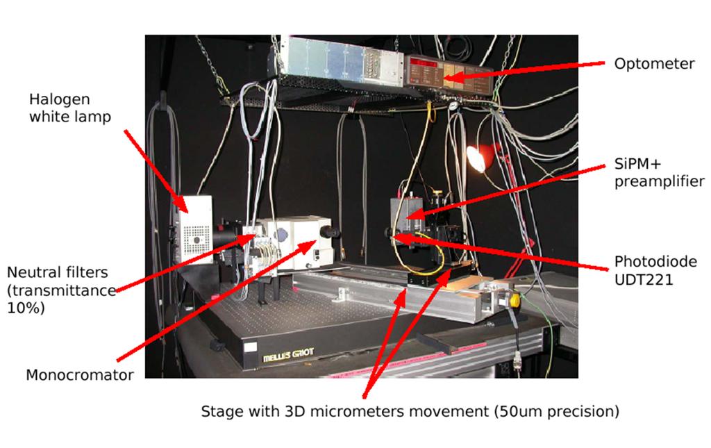
Characterisation of SiPM Index :
 Characterisation of SiPM --------------------------------------------------------------------------------------------Index : 1. Basics of SiPM* 2. SiPM module 3. Working principle 4. Experimental setup
Lithography. 3 rd. lecture: introduction. Prof. Yosi Shacham-Diamand. Fall 2004
 Lithography 3 rd lecture: introduction Prof. Yosi Shacham-Diamand Fall 2004 1 List of content Fundamental principles Characteristics parameters Exposure systems 2 Fundamental principles Aerial Image Exposure
PHGN/CHEN/MLGN 435/535: Interdisciplinary Silicon Processing Laboratory. Simple Si solar Cell!
 Where were we? Simple Si solar Cell! Two Levels of Masks - photoresist, alignment Etch and oxidation to isolate thermal oxide, deposited oxide, wet etching, dry etching, isolation schemes Doping - diffusion/ion
Silicon Photo Multiplier SiPM. Lecture 13
 Silicon Photo Multiplier SiPM Lecture 13 Photo detectors Purpose: The PMTs that are usually employed for the light detection of scintillators are large, consume high power and are sensitive to the magnetic
Nano-structured superconducting single-photon detector
 Nano-structured superconducting single-photon detector G. Gol'tsman *a, A. Korneev a,v. Izbenko a, K. Smirnov a, P. Kouminov a, B. Voronov a, A. Verevkin b, J. Zhang b, A. Pearlman b, W. Slysz b, and R.
Tutors Dominik Dannheim, Thibault Frisson (CERN, Geneva, Switzerland)
") Danube School on Instrumentation in Elementary Particle & Nuclear Physics University of Novi Sad, Serbia, September 8 th 13 th, 2014 Lab Experiment: Characterization of Silicon Photomultipliers Dominik
Danube School on Instrumentation in Elementary Particle & Nuclear Physics University of Novi Sad, Serbia, September 8 th 13 th, 2014 Lab Experiment: Characterization of Silicon Photomultipliers Dominik
Inkjet Filling of TSVs with Silver Nanoparticle Ink. Behnam Khorramdel, Matti Mäntysalo Tampere University of Technology ESTC 2014 Finland, Helsinki
 Inkjet Filling of TSVs with Silver Nanoparticle Ink Behnam Khorramdel, Matti Mäntysalo Tampere University of Technology ESTC 2014 Finland, Helsinki Outline Motivation for this study Inkjet in MEMS fabrication
Silicon Sensor and Detector Developments for the CMS Tracker Upgrade
 Silicon Sensor and Detector Developments for the CMS Tracker Upgrade Università degli Studi di Firenze and INFN Sezione di Firenze E-mail: candi@fi.infn.it CMS has started a campaign to identify the future
420 Intro to VLSI Design
 Dept of Electrical and Computer Engineering 420 Intro to VLSI Design Lecture 0: Course Introduction and Overview Valencia M. Joyner Spring 2005 Getting Started Syllabus About the Instructor Labs, Problem
REVISION #25, 12/12/2012
 HYPRES NIOBIUM INTEGRATED CIRCUIT FABRICATION PROCESS #03-10-45 DESIGN RULES REVISION #25, 12/12/2012 Direct all inquiries, questions, comments and suggestions concerning these design rules and/or HYPRES
High-Speed Scalable Silicon-MoS 2 P-N Heterojunction Photodetectors
 High-Speed Scalable Silicon-MoS 2 P-N Heterojunction Photodetectors Veerendra Dhyani 1, and Samaresh Das 1* 1 Centre for Applied Research in Electronics, Indian Institute of Technology Delhi, New Delhi-110016,
PERSPECTIVES FOR DISRUPTIVE 200MM/8-INCH GAN POWER DEVICE AND GAN-IC TECHNOLOGY DR. DENIS MARCON SR. BUSINESS DEVELOPMENT MANAGER
 PERSPECTIVES FOR DISRUPTIVE 200MM/8-INCH GAN POWER DEVICE AND GAN-IC TECHNOLOGY DR. DENIS MARCON SR. BUSINESS DEVELOPMENT MANAGER What I will show you today 200mm/8-inch GaN-on-Si e-mode/normally-off technology
Advanced ACTPol Multichroic Horn-Coupled Polarimeter Array Fabrication on 150 mm Wafers
 Advanced ACTPol Multichroic Horn-Coupled Polarimeter Array Fabrication on 150 mm Wafers Shannon M. Duff NIST for the Advanced ACTPol Collaboration LTD16 22 July 2015 Grenoble, France Why Long-λ Detectors
Andrea WILMS GSI, Helmholtzzentrum für Schwerionenforschung, Darmstadt, Germany
 GSI, Helmholtzzentrum für Schwerionenforschung, Darmstadt, Germany E-mail: A.Wilms@gsi.de During the last years the experimental demands on photodetectors used in several HEP experiments have increased
Laser patterning and projection lithography
 Introduction to Nanofabrication Techniques: Laser patterning and projection lithography Benjamin Johnston Macquarie University David O Connor Bandwidth Foundry - USYD The OptoFab node of ANFF Broad ranging
Fundamentals of CMOS Image Sensors
 CHAPTER 2 Fundamentals of CMOS Image Sensors Mixed-Signal IC Design for Image Sensor 2-1 Outline Photoelectric Effect Photodetectors CMOS Image Sensor(CIS) Array Architecture CIS Peripherals Design Considerations
EE143 Fall 2016 Microfabrication Technologies. Lecture 3: Lithography Reading: Jaeger, Chap. 2
 EE143 Fall 2016 Microfabrication Technologies Lecture 3: Lithography Reading: Jaeger, Chap. 2 Prof. Ming C. Wu wu@eecs.berkeley.edu 511 Sutardja Dai Hall (SDH) 1-1 The lithographic process 1-2 1 Photolithographic