Single Sided and Double Sided Silicon MicroStrip Detector R&D
|
|
|
- Lionel Dickerson
- 5 years ago
- Views:
Transcription
1 Single Sided and Double Sided Silicon MicroStrip Detector R&D Tariq Aziz Tata Institute, Mumbai, India SuperBelle, KEK December 10-12, 2008
2 Indian Effort Mask Design at TIFR, Processing at BEL Single Sided - 11 Sets of 32 strips with different strip width and pitch Single Sided 1024 strips with fixed strip width and pitch Double-Sided with single metal contact Double-Sided with double metal contact Wafers with different crystal orientations All on 4-inch n-type bulk wafer
3 First Batch Specifications for Prototype Single Sided Silicon Microstrip Detector Wafer : n type Silicon, 4inch Diameter, 300 micron thickness, FZ type Orientation : <111> Resistivity : 5 Kohm-cm No. Of Independent sets of detectors : 11 Type of implantation for strips : p+ No. strips per set : 32 Polysilicon resistor value: 2 to 4 Megaohms Dark Current ( at 100V reverse voltage ) max : 5 Microamps
4 Silicon Micostrip P+ Implant Details Set No. Strip length (um) width(um) Pitch(um) No. of strips
5 I V Characteristics I - V Characteristics of Silicon Microstrip Detector 600 Current ( nano amps ) Set 1 Set 2 Set 3 Set 4 Set 5 Set 6 Set 7 Set 8 Set 9 Set 10 Set Voltage ( -ve )
6 C V Characteristics C - V Characteristics 250 Capacitance ( pf ) Set 1 Set 2 Set 3 Set 4 Set 5 Set 6 Set 7 Set 8 Set 9 Set 10 Set Voltage ( -ve )
7 Second Batch Development of Single and Double Sided Silicon microstrip Detector First Processing Cycle
8 Specifications of Double Sided Silicon microstrip Detectors Wafer orientation : <100> FZ Resistivity : 10k to 20k ohm cm wafer thickness : 300 microns Poly silicon value : > 5 Mega ohms P side : Number of strips : 1024 coupling capacitance : 160 pf P+ strip width : 50 microns Pitch : 75 microns N side : Number of strips : 512 coupling capacitance : 90 pf N+ strip width : 12 microns Pitch : 50 microns Structure : ATOLL
9 Double sided silicon detector Specifications continued Wafer crystal orientation : < 100 >,Type: FZ Wafer thickness : 300 µm, Size : 4 inch Resistivity : > 5 Kohm-cm Breakdown voltage : > 300V Polysilicon resistor value : > 4 Megaohms Total Dark current : <= 2 100V Number of Dead Strips < 1% Area : x Effective Area : x Detectors Produced : 1) SSD - 5 No s 2) DSSD SL - 10 No s 3) DSSD DL - 10 No s
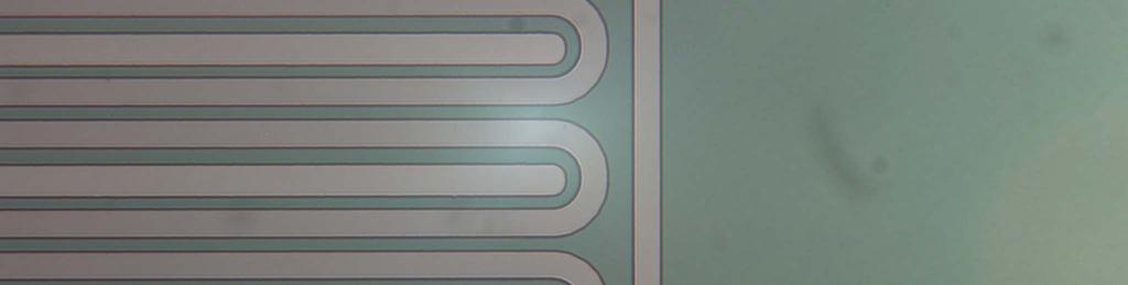
10 First Process Cycle I V Characteristics Single sided detector <100 > 300 Current ( microamps ) Det 56 Det 63 Det 49 Det 57 Det Voltage ( volts ) Leakage current higher than expected BEL need to modify process parameters
11 Coupling capacitance coupling capacitance capacitance ( pf ) Series voltage Spec- 160 pf Reasonably close, Need to do better
12 C V characteristics C - V characteristics ( Bulk ) Capacitance ( pf ) voltage Series1 Higher than expected, Need to optimize process parameters


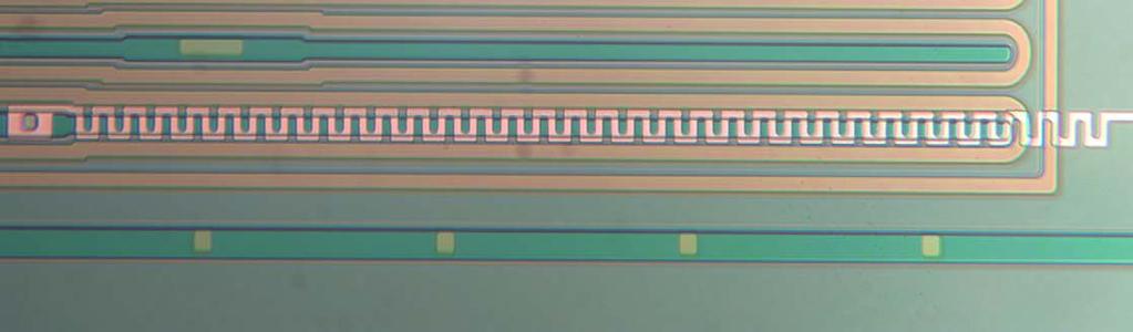
13 Double Sided Photo N Side Polysilicon resistors


14 N side ATOLL structure

15 N - Side AC pads

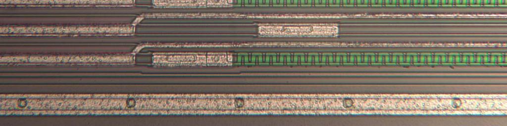
16 N Side DC pads

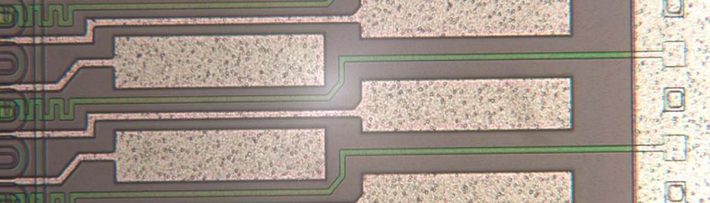
17 P side design with all masks


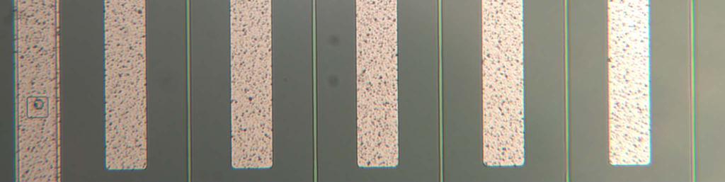
18 P side single metal AC pads

19 Photo of P - side Via s and Metal 2 Via s


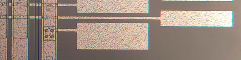
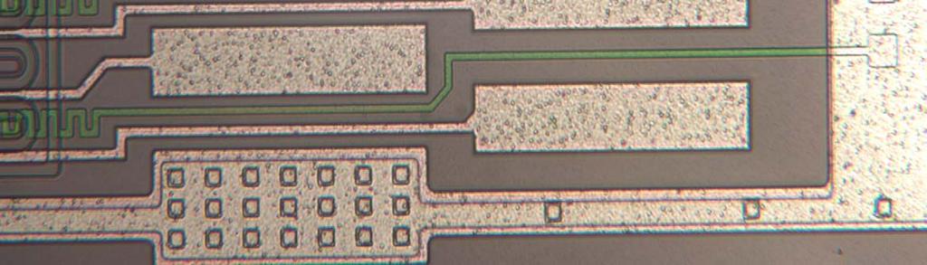
20 P side AC pads after double metal


21 P side double metal structure
22 Double sided silicon detector photo
23 I V characteristics of Double sided silicon Microstip detectors Double sided detector <100> I - V characteristics DSSD-DL Current ( microamps ) DSSD-SL DSSD-SL DSSD-DL Voltage Leakage current significantly higher than expected First Process Cycle
24 I V Comparision of single sided and double sided detectors Double sided detector <100> I - V Characteristics 350 Current ( micro amps ) DSSD-DL DSSD-SL SSD SSD#63 DSSD-SL#28 DSSD-DL # Voltage ( volts ) First Process Cycle
25 Third Batch Development of single sided silicon microstrip detector Number of detectors developed : 5 Wafer orientation : <111> FZ (earlier 100) Resistivity : 9k to 12k ohm cm wafer thickness : 300 microns Poly silicon value : > 5 Mega ohms Number of strips : 1024 coupling capacitance : 160 pf P+ strip width : 50 microns Pitch : 75 microns Dead strip fraction : < 1%
26 I V characteristics of single sided detectors with different poly-values Poly-values Achieved : SSD # 1 20 Mega ohms New <111> SSD Bulk I - V SSD # 3 9 Giga ohms 40 SSD # 4 30 Mega hms SSD # 5 26 Mega ohms Current ( ua ) SSD 5 SSD 1 SSD 3 SSD voltage
27 Fourth Batch Under Development Single sided silicon detector development with low resistivity of 2 to 4k ohm - cm Expect first cycle by December end If we see better results compared to high resistivity then go for DSSD as well
28 Remarks DSSD Mask Design concept seems fine Double Metal contact works Leakage current and Capacitance on higher side Since this is first cycle, hope better results at the end of 5 th cycle in about a year Pin-holes better than before, Need to do still better
29 Extra Slides
30 DOUBLE SIDED SILICON MICRO STRIP DETECTORS Wafer crystal orientation : < 100 > Type : FZ Wafer thickness : 300 µm Size : 4 inch Resistivity : > 5 Kohm-cm Breakdown voltage : > 300V Polysilicon resistor value : > 4 Megaohms Total Dark current : <= 2 100V Area : x Effective Area : x 25600
31 N side : Number of strips : 512 Pitch : 50 N+ strip width : 12 N+ strip length : P stop with ATTOL structure AC pads will be available on both sides of the strips. Polyresistors will be placed for one strip on the left side and the adjacent strip on the other side. Proving pad ( N sub )
32 P side : Number of strips : 1024 Number of Readout strips : 512 Pitch : 75 P+ strip width : 50 P+ strip length : Readout strips will be 512 only for both double metal structure as well as without double metal structure AC pads will be available on both sides of the strips but reading will be alternate strips only With double metal structure readout will be 512 strips Polyresistors will be placed for one strip on one side and the adjacent strip on the other side. AC pad accessibility of the strips will be available with double metal structure and as well as without double metal structure ( provision for bonding with kepton cable) Proving pad ( N sub ) and serial number of strips on both sides
33 Silicon strip devices: Principle of operation Basic motivation: charged particle position measurement Use ionization signal left behind by charged particle passage In a solid semiconductor, ionization produces electrons-hole pairs. For Si need 3.6 ev to produce one e-h pair. In pure Si, e-h pairs quickly recombine need to drift the charges to electrodes but how?
34 Construction of detector Sensor design choices Sensor design must first follow physics requirements, still many choices: Geometrical shape Double-sided or singlesided Thickness Read-out and implant Type of biasing structure pitch AC or DC coupling p or n bulk silicon, Double-metal read-out resistivity In many cases there are conflicting design trade-offs between these choices. One finds that economics (limited project budget) often forces decision direction. Examples of trade-offs: Choice Pro Con Double-sided sensor Less material for two read-out coordinates Processing cost about 3x that for single-sided 500μm thickness More signal Multiple scattering and material budget are more
35 Principle of operation Properties of the depletion zone Depletion width is a function of the bulk resistivity, charge carrier mobility μ and the magnitude of the reverse bias voltage V b : w = 2ερμV b V b + Depletion zone undepleted zone w d where ρ = 1/qμN for doped materiel and N is the doping concentration (q is always the charge of the electron) The voltage needed to completely deplete a device of thickness d is called the depletion voltage, V d V d =d 2 / (2ερμ) Thus one needs a higher voltage to fully deplete a low resistivity material. One also sees that a higher voltage is needed for a p-type bulk since the carrier mobility of holes is lower than for electrons (450 vs 1350 cm 2 / V s)

 Mask 6 : Metal Mask3 :")

36 MASK DESIGNS Mask 1 : p+ Mask 5 : Opening Contacts over dc pad, bias pad Mask2 : Capacitor (Sio 2 ) Mask 6 : Metal Mask3 : Polycontact opening Mask 7 : Protective layer Mask4 : Polyresistor
37 Principle of operation Properties of the depletion zone (cont) The capacitance is simply the parallel plate capacity of the depletion zone. One normally measures the depletion behaviour (finds the depletion voltage) by measuring the capacitance versus reverse bias voltage. C = A ε / 2ρμV b capacitance vs voltage
38 Principle of operation Charge collection Need to isolate strips from each other and collect/measure charge on each strip high impedance bias connection (resistor or equivalent) Usually want to AC couple input amplifier to avoid large DC input currents Both of these structures are often integrated directly on the silicon sensor. Bias resistors via deposition of doped polysilicon, and capacitors via metal readout lines over the implants but separated by an insulating dielectric layer (SiO 2 ). + h+ e- Minimum ionizing particle generates approximately electron hole pairs in 300micron silicon detector

39 ProtoType Silicon Microstrip Detector Geometry : 76mm * 47mm
Design, fabrication and characterization of the first AC-coupled silicon microstrip sensors in India
 arxiv:1402.2406 [physics.ins-det] Design, fabrication and characterization of the first AC-coupled silicon microstrip sensors in India T. Aziz, a S.R. Chendvankar, a G.B. Mohanty, a, M.R. Patil, a K.K.
Development of Double-sided Silcon microstrip Detector. D.H. Kah*, H. Park, H.J. Kim (BAERI JikLee (SNU) E. Won (Korea U)
 E. Won (Korea U)") Development of Double-sided Silcon microstrip Detector D.H. Kah*, H. Park, H.J. Kim (BAERI JikLee (SNU) E. Won (Korea U), KNU) 2005 APPI dhkah@belle.knu.ac.kr 1 1. Motivation 2. Introduction Contents 1.
Development of Double-sided Silcon microstrip Detector D.H. Kah*, H. Park, H.J. Kim (BAERI JikLee (SNU) E. Won (Korea U), KNU) 2005 APPI dhkah@belle.knu.ac.kr 1 1. Motivation 2. Introduction Contents 1.
irst: process development, characterization and first irradiation studies
 3D D detectors at ITC-irst irst: process development, characterization and first irradiation studies S. Ronchin a, M. Boscardin a, L. Bosisio b, V. Cindro c, G.-F. Dalla Betta d, C. Piemonte a, A. Pozza
Silicon Detectors in High Energy Physics
 Thomas Bergauer (HEPHY Vienna) IPM Teheran 22 May 2011 Sunday: Schedule Semiconductor Basics (45 ) Silicon Detectors in Detector concepts: Pixels and Strips (45 ) Coffee Break Strip Detector Performance
Integrated diodes. The forward voltage drop only slightly depends on the forward current. ELEKTRONIKOS ĮTAISAI
 1 Integrated diodes pn junctions of transistor structures can be used as integrated diodes. The choice of the junction is limited by the considerations of switching speed and breakdown voltage. The forward
Simulation and test of 3D silicon radiation detectors
 Simulation and test of 3D silicon radiation detectors C.Fleta 1, D. Pennicard 1, R. Bates 1, C. Parkes 1, G. Pellegrini 2, M. Lozano 2, V. Wright 3, M. Boscardin 4, G.-F. Dalla Betta 4, C. Piemonte 4,
Simulation of High Resistivity (CMOS) Pixels
 Pixels") Simulation of High Resistivity (CMOS) Pixels Stefan Lauxtermann, Kadri Vural Sensor Creations Inc. AIDA-2020 CMOS Simulation Workshop May 13 th 2016 OUTLINE 1. Definition of High Resistivity Pixel Also
Simulation of High Resistivity (CMOS) Pixels Stefan Lauxtermann, Kadri Vural Sensor Creations Inc. AIDA-2020 CMOS Simulation Workshop May 13 th 2016 OUTLINE 1. Definition of High Resistivity Pixel Also
Silicon Sensor Developments for the CMS Tracker Upgrade
 Silicon Sensor Developments for the CMS Tracker Upgrade on behalf of the CMS tracker collaboration University of Hamburg, Germany E-mail: Joachim.Erfle@desy.de CMS started a campaign to identify the future
Thin Silicon R&D for LC applications
 Thin Silicon R&D for LC applications D. Bortoletto Purdue University Status report Hybrid Pixel Detectors for LC Next Linear Collider:Physic requirements Vertexing 10 µ mgev σ r φ,z(ip ) 5µ m 3 / 2 p sin
Gamma-ray Large Area Space Telescope (GLAST) Large Area Telescope (LAT) Silicon Detector Specification
 Large Area Telescope (LAT) Silicon Detector Specification") GLAST LAT PROCUREMENT SPECIFICATION Document # Document Title GLAST LAT Silicon Detector Specification Date Effective Page 1 of 21 GE-00011-A 1rst Draft 8/20/00 Author(s) Supersedes H. Sadrozinski T. Ohsugi
GLAST LAT PROCUREMENT SPECIFICATION Document # Document Title GLAST LAT Silicon Detector Specification Date Effective Page 1 of 21 GE-00011-A 1rst Draft 8/20/00 Author(s) Supersedes H. Sadrozinski T. Ohsugi
Semiconductor Detector Systems
 Semiconductor Detector Systems Helmuth Spieler Physics Division, Lawrence Berkeley National Laboratory OXFORD UNIVERSITY PRESS ix CONTENTS 1 Detector systems overview 1 1.1 Sensor 2 1.2 Preamplifier 3
UNIVERSITY of CALIFORNIA SANTA CRUZ
 UNIVERSITY of CALIFORNIA SANTA CRUZ CHARACTERIZATION OF THE IRST PROTOTYPE P-TYPE SILICON STRIP SENSOR A thesis submitted in partial satisfaction of the requirements for the degree of BACHELOR OF SCIENCE
Semiconductor Devices Lecture 5, pn-junction Diode
 Semiconductor Devices Lecture 5, pn-junction Diode Content Contact potential Space charge region, Electric Field, depletion depth Current-Voltage characteristic Depletion layer capacitance Diffusion capacitance
Solid State Devices- Part- II. Module- IV
 Solid State Devices- Part- II Module- IV MOS Capacitor Two terminal MOS device MOS = Metal- Oxide- Semiconductor MOS capacitor - the heart of the MOSFET The MOS capacitor is used to induce charge at the
Figure Responsivity (A/W) Figure E E-09.
 Figure E E-09.") OSI Optoelectronics, is a leading manufacturer of fiber optic components for communication systems. The products offer range for Silicon, GaAs and InGaAs to full turnkey solutions. Photodiodes are semiconductor
OSI Optoelectronics, is a leading manufacturer of fiber optic components for communication systems. The products offer range for Silicon, GaAs and InGaAs to full turnkey solutions. Photodiodes are semiconductor
Simulation of new P-type strip detectors with trench to enhance the charge multiplication effect in the n- type electrodes
 Simulation of new P-Type strip detectors RESMDD 10, Florence 12-15.October.2010 1/15 Simulation of new P-type strip detectors with trench to enhance the charge multiplication effect in the n- type electrodes
Semiconductor Physics and Devices
 Metal-Semiconductor and Semiconductor Heterojunctions The Metal-Oxide-Semiconductor Field-Effect Transistor (MOSFET) is one of two major types of transistors. The MOSFET is used in digital circuit, because
Strip Detectors. Principal: Silicon strip detector. Ingrid--MariaGregor,SemiconductorsasParticleDetectors. metallization (Al) p +--strips
 p +--strips") Strip Detectors First detector devices using the lithographic capabilities of microelectronics First Silicon detectors -- > strip detectors Can be found in all high energy physics experiments of the last
Strip Detectors First detector devices using the lithographic capabilities of microelectronics First Silicon detectors -- > strip detectors Can be found in all high energy physics experiments of the last
Figure Figure E E-09. Dark Current (A) 1.
 1.") OSI Optoelectronics, is a leading manufacturer of fiber optic components for communication systems. The products offer range for Silicon, GaAs and InGaAs to full turnkey solutions. Photodiodes are semiconductor
OSI Optoelectronics, is a leading manufacturer of fiber optic components for communication systems. The products offer range for Silicon, GaAs and InGaAs to full turnkey solutions. Photodiodes are semiconductor
FET(Field Effect Transistor)
") Field Effect Transistor: Construction and Characteristic of JFETs. Transfer Characteristic. CS,CD,CG amplifier and analysis of CS amplifier MOSFET (Depletion and Enhancement) Type, Transfer Characteristic,
Field Effect Transistor: Construction and Characteristic of JFETs. Transfer Characteristic. CS,CD,CG amplifier and analysis of CS amplifier MOSFET (Depletion and Enhancement) Type, Transfer Characteristic,
HMPP-386x Series MiniPak Surface Mount RF PIN Diodes
 HMPP-86x Series MiniPak Surface Mount RF PIN Diodes Data Sheet Description/Applications These ultra-miniature products represent the blending of Avago Technologies proven semiconductor and the latest in
Silicon sensors for radiant signals. D.Sc. Mikko A. Juntunen
 Silicon sensors for radiant signals D.Sc. Mikko A. Juntunen 2017 01 16 Today s outline Introduction Basic physical principles PN junction revisited Applications Light Ionizing radiation X-Ray sensors in
Integrated Circuits: FABRICATION & CHARACTERISTICS - 4. Riju C Issac
 Integrated Circuits: FABRICATION & CHARACTERISTICS - 4 Riju C Issac INTEGRATED RESISTORS Resistor in a monolithic IC is very often obtained by the bulk resistivity of one of the diffused areas. P-type
EDC Lecture Notes UNIT-1
 P-N Junction Diode EDC Lecture Notes Diode: A pure silicon crystal or germanium crystal is known as an intrinsic semiconductor. There are not enough free electrons and holes in an intrinsic semi-conductor
INTRODUCTION: Basic operating principle of a MOSFET:
 INTRODUCTION: Along with the Junction Field Effect Transistor (JFET), there is another type of Field Effect Transistor available whose Gate input is electrically insulated from the main current carrying
Analog Electronic Circuits
 Analog Electronic Circuits Chapter 1: Semiconductor Diodes Objectives: To become familiar with the working principles of semiconductor diode To become familiar with the design and analysis of diode circuits
SIM-Detecteurs 2014 LPNHE-Paris
 SIM-Detecteurs 2014 LPNHE-Paris The application of Silvaco process and device simulation program to the development of silicon detector for the high energy particle detection Li Long llong@cismst.de CiS
INTRODUCTION TO MOS TECHNOLOGY
 INTRODUCTION TO MOS TECHNOLOGY 1. The MOS transistor The most basic element in the design of a large scale integrated circuit is the transistor. For the processes we will discuss, the type of transistor
AE53/AC53/AT53/AE103 ELECT. DEVICES & CIRCUITS DEC 2015
 Q.2 a. By using Norton s theorem, find the current in the load resistor R L for the circuit shown in Fig.1. (8) Fig.1 IETE 1 b. Explain Z parameters and also draw an equivalent circuit of the Z parameter
Department of Electrical Engineering IIT Madras
 Department of Electrical Engineering IIT Madras Sample Questions on Semiconductor Devices EE3 applicants who are interested to pursue their research in microelectronics devices area (fabrication and/or
Role of guard rings in improving the performance of silicon detectors
 PRAMANA c Indian Academy of Sciences Vol. 65, No. 2 journal of August 2005 physics pp. 259 272 Role of guard rings in improving the performance of silicon detectors VIJAY MISHRA, V D SRIVASTAVA and S K
 Electronic Devices 1. Current flowing in each of the following circuits A and respectively are: (Circuit 1) (Circuit 2) 1) 1A, 2A 2) 2A, 1A 3) 4A, 2A 4) 2A, 4A 2. Among the following one statement is not
Design and Simulation of a Silicon Photomultiplier Array for Space Experiments
 Journal of the Korean Physical Society, Vol. 52, No. 2, February 2008, pp. 487491 Design and Simulation of a Silicon Photomultiplier Array for Space Experiments H. Y. Lee, J. Lee, J. E. Kim, S. Nam, I.
Development of a large area silicon pad detector for the identification of cosmic ions
 Development of a large area silicon pad detector for the identification of cosmic ions M.Y. Kim 1,2 P.S. Marrocchesi 1, C. Avanzini 2, M.G. Bagliesi 1, G. Bigongiari 1,A. Caldarone 1,R. Cecchi 1,, P. Maestro
Mechanis m Faliures. Group Leader Jepsy 1)Substrate Biasing 2) Minority Injection. Bob 1)Minority-Carrier Guard Rings
Substrate Biasing 2) Minority Injection. Bob 1)Minority-Carrier Guard Rings") Mechanis m Faliures Group Leader Jepsy 1)Substrate Biasing 2) Minority Injection As im 1)Types Of Guard Rings Sandra 1)Parasitics 2)Field Plating Bob 1)Minority-Carrier Guard Rings Shawn 1)Parasitic Channel
Mechanis m Faliures Group Leader Jepsy 1)Substrate Biasing 2) Minority Injection As im 1)Types Of Guard Rings Sandra 1)Parasitics 2)Field Plating Bob 1)Minority-Carrier Guard Rings Shawn 1)Parasitic Channel
Three Terminal Devices
 Three Terminal Devices - field effect transistor (FET) - bipolar junction transistor (BJT) - foundation on which modern electronics is built - active devices - devices described completely by considering
A new Vertical JFET Technology for Harsh Radiation Applications
 A New Vertical JFET Technology for Harsh Radiation Applications ISPS 2016 1 A new Vertical JFET Technology for Harsh Radiation Applications A Rad-Hard switch for the ATLAS Inner Tracker P. Fernández-Martínez,
Physics 160 Lecture 5. R. Johnson April 13, 2015
 Physics 160 Lecture 5 R. Johnson April 13, 2015 Half Wave Diode Rectifiers Full Wave April 13, 2015 Physics 160 2 Note that there is no ground connection on this side of the rectifier! Output Smoothing
MOSFET & IC Basics - GATE Problems (Part - I)
") MOSFET & IC Basics - GATE Problems (Part - I) 1. Channel current is reduced on application of a more positive voltage to the GATE of the depletion mode n channel MOSFET. (True/False) [GATE 1994: 1 Mark]
MOSFET & IC Basics - GATE Problems (Part - I) 1. Channel current is reduced on application of a more positive voltage to the GATE of the depletion mode n channel MOSFET. (True/False) [GATE 1994: 1 Mark]
Ch5 Diodes and Diodes Circuits
 Circuits and Analog Electronics Ch5 Diodes and Diodes Circuits 5.1 The Physical Principles of Semiconductor 5.2 Diodes 5.3 Diode Circuits 5.4 Zener Diode References: Floyd-Ch2; Gao-Ch6; 5.1 The Physical
EE 5611 Introduction to Microelectronic Technologies Fall Thursday, September 04, 2014 Lecture 02
 EE 5611 Introduction to Microelectronic Technologies Fall 2014 Thursday, September 04, 2014 Lecture 02 1 Lecture Outline Review on semiconductor materials Review on microelectronic devices Example of microelectronic
ECE 340 Lecture 37 : Metal- Insulator-Semiconductor FET Class Outline:
 ECE 340 Lecture 37 : Metal- Insulator-Semiconductor FET Class Outline: Metal-Semiconductor Junctions MOSFET Basic Operation MOS Capacitor Things you should know when you leave Key Questions What is the
Class XII - Physics Semiconductor Electronics. Chapter-wise Problems
 lass X - Physics Semiconductor Electronics Materials, Device and Simple ircuit hapter-wise Problems Multiple hoice Question :- 14.1 The conductivity of a semiconductor increases with increase in temperature
In this lecture we will begin a new topic namely the Metal-Oxide-Semiconductor Field Effect Transistor.
 Solid State Devices Dr. S. Karmalkar Department of Electronics and Communication Engineering Indian Institute of Technology, Madras Lecture - 38 MOS Field Effect Transistor In this lecture we will begin
Lecture 2. Part 2 (Semiconductor detectors =sensors + electronics) Segmented detectors with pn-junction. Strip/pixel detectors
 Segmented detectors with pn-junction. Strip/pixel detectors") Lecture 2 Part 1 (Electronics) Signal formation Readout electronics Noise Part 2 (Semiconductor detectors =sensors + electronics) Segmented detectors with pn-junction Strip/pixel detectors Drift detectors
Lecture 2 Part 1 (Electronics) Signal formation Readout electronics Noise Part 2 (Semiconductor detectors =sensors + electronics) Segmented detectors with pn-junction Strip/pixel detectors Drift detectors
NAME: Last First Signature
 UNIVERSITY OF CALIFORNIA, BERKELEY College of Engineering Department of Electrical Engineering and Computer Sciences EE 130: IC Devices Spring 2003 FINAL EXAMINATION NAME: Last First Signature STUDENT
10/27/2009 Reading: Chapter 10 of Hambley Basic Device Physics Handout (optional)
") EE40 Lec 17 PN Junctions Prof. Nathan Cheung 10/27/2009 Reading: Chapter 10 of Hambley Basic Device Physics Handout (optional) Slide 1 PN Junctions Semiconductor Physics of pn junctions (for reference
EE40 Lec 17 PN Junctions Prof. Nathan Cheung 10/27/2009 Reading: Chapter 10 of Hambley Basic Device Physics Handout (optional) Slide 1 PN Junctions Semiconductor Physics of pn junctions (for reference
CMOS 0.18 m SPAD. TowerJazz February, 2018 Dr. Amos Fenigstein
 CMOS 0.18 m SPAD TowerJazz February, 2018 Dr. Amos Fenigstein Outline CMOS SPAD motivation Two ended vs. Single Ended SPAD (bulk isolated) P+/N two ended SPAD and its optimization Application of P+/N two
Lecture - 18 Transistors
 Electronic Materials, Devices and Fabrication Dr. S. Prarasuraman Department of Metallurgical and Materials Engineering Indian Institute of Technology, Madras Lecture - 18 Transistors Last couple of classes
Characteristics of the ALICE Silicon Drift Detector.
 Characteristics of the ALICE Silicon Drift Detector. A. Rashevsky b,1, V. Bonvicini b, P. Burger c, P. Cerello a, E. Crescio a, P. Giubellino a, R. Hernández-Montoya a,2, A. Kolojvari a,3, L.M. Montaño
Lecture #29. Moore s Law
 Lecture #29 ANNOUNCEMENTS HW#15 will be for extra credit Quiz #6 (Thursday 5/8) will include MOSFET C-V No late Projects will be accepted after Thursday 5/8 The last Coffee Hour will be held this Thursday
3-D Modelling of the Novel Nanoscale Screen-Grid Field Effect Transistor (SGFET)
") 3-D Modelling of the Novel Nanoscale Screen-Grid Field Effect Transistor (SGFET) Pei W. Ding, Kristel Fobelets Department of Electrical Engineering, Imperial College London, U.K. J. E. Velazquez-Perez
3-D Modelling of the Novel Nanoscale Screen-Grid Field Effect Transistor (SGFET) Pei W. Ding, Kristel Fobelets Department of Electrical Engineering, Imperial College London, U.K. J. E. Velazquez-Perez
CMOS Detectors Ingeniously Simple!
 CMOS Detectors Ingeniously Simple! A.Schöning University Heidelberg B-Workshop Neckarzimmern 18.-20.2.2015 1 Detector System on Chip? 2 ATLAS Pixel Module 3 ATLAS Pixel Module MCC sensor FE-Chip FE-Chip
Production of HPDs for the LHCb RICH Detectors
 Production of HPDs for the LHCb RICH Detectors LHCb RICH Detectors Hybrid Photon Detector Production Photo Detector Test Facilities Test Results Conclusions IEEE Nuclear Science Symposium Wyndham, 24 th
BJT. Bipolar Junction Transistor BJT BJT 11/6/2018. Dr. Satish Chandra, Assistant Professor, P P N College, Kanpur 1
 BJT Bipolar Junction Transistor Satish Chandra Assistant Professor Department of Physics P P N College, Kanpur www.satish0402.weebly.com The Bipolar Junction Transistor is a semiconductor device which
LAB MANUAL. CV/IV Static Characterization Methods
 LAB MANUAL CV/IV Static Characterization Methods Centre for Detector & Related Software Technology (CDRST) Department of Physics & Astrophysics, University of Delhi INTRODUCTION 1.1. Silicon Detector Particle
Recent Technological Developments on LGAD and ilgad Detectors for Tracking and Timing Applications
 Recent Technological Developments on LGAD and ilgad Detectors for Tracking and Timing Applications G. Pellegrini 1, M. Baselga 1, M. Carulla 1, V. Fadeyev 2, P. Fernández-Martínez 1, M. Fernández García
Wiring Parasitics. Contact Resistance Measurement and Rules
 Wiring Parasitics Contact Resistance Measurement and Rules Connections between metal layers and nonmetal layers are called contacts. Connections between metal layers are called vias. For non-critical design,
Status of ITC-irst activities in RD50
 Status of ITC-irst activities in RD50 M. Boscardin ITC-irst, Microsystem Division Trento, Italy Outline Materials/Pad Detctors Pre-irradiated silicon INFN Padova and Institute for Nuclear Research of NASU,
Leakage Current Prediction for GLAST Silicon Detectors
 SCIPP 97/16 Leakage Current Prediction for GLAST Silicon Detectors T. Dubbs, H.F.-W Sadrozinski, S. Kashigan, W. Kroeger, S. Jaggar, R.Johnson, W. Rowe, A. Webster SCIPP, University of California Santa
Design Simulation and Analysis of NMOS Characteristics for Varying Oxide Thickness
 MIT International Journal of Electronics and Communication Engineering, Vol. 4, No. 2, August 2014, pp. 81 85 81 Design Simulation and Analysis of NMOS Characteristics for Varying Oxide Thickness Alpana
Copyright -International Centre for Diffraction Data 2010 ISSN
 234 BRIDGING THE PRICE/PERFORMANCE GAP BETWEEN SILICON DRIFT AND SILICON PIN DIODE DETECTORS Derek Hullinger, Keith Decker, Jerry Smith, Chris Carter Moxtek, Inc. ABSTRACT Use of silicon drift detectors
SSD Development for the ATLAS Upgrade Tracker
 SSD Development for the ATLAS Upgrade Tracker Meeting Mo., Feb. 26, 2007. 2-6 pm; CERN Rm. 13-3-005 ATL-P-MN-0006 v.1 Development of non-inverting Silicon strip detectors for the ATLAS ID Upgrade 1) DC
Lecture 020 ECE4430 Review II (1/5/04) Page 020-1
 Page 020-1") Lecture 020 ECE4430 Review II (1/5/04) Page 020-1 LECTURE 020 ECE 4430 REVIEW II (READING: GHLM - Chap. 2) Objective The objective of this presentation is: 1.) Identify the prerequisite material as taught
Lecture 020 ECE4430 Review II (1/5/04) Page 020-1 LECTURE 020 ECE 4430 REVIEW II (READING: GHLM - Chap. 2) Objective The objective of this presentation is: 1.) Identify the prerequisite material as taught
CCD and CMOS Imaging Devices for Large (Ground Based) Telescopes. Veljko Radeka BNL SNIC April 3, 2006
 Telescopes. Veljko Radeka BNL SNIC April 3, 2006") CCD and CMOS Imaging Devices for Large (Ground Based) Telescopes Veljko Radeka BNL SNIC April 3, 2006 1 Large Telescopes Survey telescope Deep probe Primary Mirror dia.=d m, Area= A Large (~8m) Very large
CCD and CMOS Imaging Devices for Large (Ground Based) Telescopes Veljko Radeka BNL SNIC April 3, 2006 1 Large Telescopes Survey telescope Deep probe Primary Mirror dia.=d m, Area= A Large (~8m) Very large
SRM INSTITUTE OF SCIENCE AND TECHNOLOGY (DEEMED UNIVERSITY)
") SRM INSTITUTE OF SCIENCE AND TECHNOLOGY (DEEMED UNIVERSITY) QUESTION BANK I YEAR B.Tech (II Semester) ELECTRONIC DEVICES (COMMON FOR EC102, EE104, IC108, BM106) UNIT-I PART-A 1. What are intrinsic and
SRM INSTITUTE OF SCIENCE AND TECHNOLOGY (DEEMED UNIVERSITY) QUESTION BANK I YEAR B.Tech (II Semester) ELECTRONIC DEVICES (COMMON FOR EC102, EE104, IC108, BM106) UNIT-I PART-A 1. What are intrinsic and
Solid State Device Fundamentals
 Solid State Device Fundamentals 4.4. Field Effect Transistor (MOSFET) ENS 463 Lecture Course by Alexander M. Zaitsev alexander.zaitsev@csi.cuny.edu Tel: 718 982 2812 4N101b 1 Field-effect transistor (FET)
UNIT-VI FIELD EFFECT TRANSISTOR. 1. Explain about the Field Effect Transistor and also mention types of FET s.
 UNIT-I FIELD EFFECT TRANSISTOR 1. Explain about the Field Effect Transistor and also mention types of FET s. The Field Effect Transistor, or simply FET however, uses the voltage that is applied to their
Light gathering Power: Magnification with eyepiece:
 Telescopes Light gathering Power: The amount of light that can be gathered by a telescope in a given amount of time: t 1 /t 2 = (D 2 /D 1 ) 2 The larger the diameter the smaller the amount of time. If
Basic Fabrication Steps
 Basic Fabrication Steps and Layout Somayyeh Koohi Department of Computer Engineering Adapted with modifications from lecture notes prepared by author Outline Fabrication steps Transistor structures Transistor
Università degli Studi di Roma Tor Vergata Dipartimento di Ingegneria Elettronica. Analogue Electronics. Paolo Colantonio A.A.
 Università degli Studi di Roma Tor Vergata Dipartimento di Ingegneria Elettronica Analogue Electronics Paolo Colantonio A.A. 2015-16 Introduction: materials Conductors e.g. copper or aluminum have a cloud
Optical Receivers Theory and Operation
 Optical Receivers Theory and Operation Photo Detectors Optical receivers convert optical signal (light) to electrical signal (current/voltage) Hence referred O/E Converter Photodetector is the fundamental
due to power supply and technology. Process specifications were obtained from the MOSIS
 design number 85739 VLSI Design Chromatic Instrument Tuner For the design of the operational amplifier, we have to take into consideration the constraints due to power supply and technology. Process specifications
STUDIES OF THE SILICON DRIFT DETECTOR: DESIGN, TECHNOLOGY DEVELOPMENT, CHARACTERIZATION AND PHYSICS SIMULATIONS
 , pp. 175-192 STUDIES OF THE SILICON DRIFT DETECTOR: DESIGN, TECHNOLOGY DEVELOPMENT, CHARACTERIZATION AND PHYSICS SIMULATIONS Pourus Mehta*, K.M. Sudheer, V.D. Srivastava, V.B. Chandratre, C.K. Pithawa
I E I C since I B is very small
 Figure 2: Symbols and nomenclature of a (a) npn and (b) pnp transistor. The BJT consists of three regions, emitter, base, and collector. The emitter and collector are usually of one type of doping, while
Noise Performance Analysis for the Silicon Tracking System Detector and Front-End Electronics
 Noise Performance Analysis for the Silicon Tracking System Detector and Front-End Electronics Weronika Zubrzycka, Krzysztof Kasiński zubrzycka@agh.edu.pl, kasinski@agh.edu.pl Department of Measurement
Characterization of Pre- and Post-Gamma Irradiated Mini. Silicon Strip Detectors
 Characterization of Pre- and Post-Gamma Irradiated Mini Silicon Strip Detectors A Thesis Submitted in Partial Satisfaction of the Requirements for the Degree of BACHELOR OF SCIENCE in APPLIED PHYSICS at
The current density at a forward bias of 0.9 V is J( V) = 8:91 10 ;13 exp 0:06 = 9: :39=961:4 Acm ; 1: 10 ;8 exp 0:05 The current is dominated b
 = 8:91 10 ;13 exp 0:06 = 9: :39=961:4 Acm ; 1: 10 ;8 exp 0:05 The current is dominated b") Prof. Jasprit Singh Fall 000 EECS 30 Solutions to Homework 6 Problem 1 Two dierent processes are used to fabricate a Si p-n diode. The rst process results in a electron-hole recombination time via impurities
Prof. Jasprit Singh Fall 000 EECS 30 Solutions to Homework 6 Problem 1 Two dierent processes are used to fabricate a Si p-n diode. The rst process results in a electron-hole recombination time via impurities
Transistor was first invented by William.B.Shockley, Walter Brattain and John Bardeen of Bell Labratories. In 1961, first IC was introduced.
 Unit 1 Basic MOS Technology Transistor was first invented by William.B.Shockley, Walter Brattain and John Bardeen of Bell Labratories. In 1961, first IC was introduced. Levels of Integration:- i) SSI:-
Fabrication, Corner, Layout, Matching, & etc.
 Advanced Analog Building Blocks Fabrication, Corner, Layout, Matching, & etc. Wei SHEN (KIP) 1 Fabrication Steps for MOS Wei SHEN, Universität Heidelberg 2 Fabrication Steps for MOS Wei SHEN, Universität
Unit III FET and its Applications. 2 Marks Questions and Answers
 Unit III FET and its Applications 2 Marks Questions and Answers 1. Why do you call FET as field effect transistor? The name field effect is derived from the fact that the current is controlled by an electric
Chap14. Photodiode Detectors
 Chap14. Photodiode Detectors Mohammad Ali Mansouri-Birjandi mansouri@ece.usb.ac.ir mamansouri@yahoo.com Faculty of Electrical and Computer Engineering University of Sistan and Baluchestan (USB) Design
Organic Electronics. Information: Information: 0331a/ 0442/
 Organic Electronics (Course Number 300442 ) Spring 2006 Organic Field Effect Transistors Instructor: Dr. Dietmar Knipp Information: Information: http://www.faculty.iubremen.de/course/c30 http://www.faculty.iubremen.de/course/c30
Frequency Response Properties of the Silicon Vertex Detector for BaBar
 Frequency Response Properties of the Silicon Vertex Detector for BaBar Lawrence Lin Jeff Richman Sam Burke UCSB Summer 2001 Contents 1 Introduction 2 2 p-side of the Detector 3 3 n-side of the Detector
Lecture 2 p-n junction Diode characteristics. By Asst. Prof Dr. Jassim K. Hmood
 Electronic I Lecture 2 p-n junction Diode characteristics By Asst. Prof Dr. Jassim K. Hmood THE p-n JUNCTION DIODE The pn junction diode is formed by fabrication of a p-type semiconductor region in intimate
IV curves of different pixel cells
 IV curves of different pixel cells 6 5 100 µm pitch, 10µm gap 100 µm pitch, 50µm gap current [pa] 4 3 2 1 interface generation current volume generation current 0 0 50 100 150 200 250 bias voltage [V]
Electronics I. Midterm #1
 The University of Toledo s6ms_elct7.fm - Electronics I Midterm # Problems Points. 4 2. 5 3. 6 Total 5 Was the exam fair? yes no The University of Toledo s6ms_elct7.fm - 2 Problem 4 points For full credit,
The HGTD: A SOI Power Diode for Timing Detection Applications
 The HGTD: A SOI Power Diode for Timing Detection Applications Work done in the framework of RD50 Collaboration (CERN) M. Carulla, D. Flores, S. Hidalgo, D. Quirion, G. Pellegrini IMB-CNM (CSIC), Spain
Lecture 3: Diodes. Amplitude Modulation. Diode Detection.
 Whites, EE 322 Lecture 3 Page 1 of 10 Lecture 3: Diodes. Amplitude Modulation. Diode Detection. Diodes are the fourth basic discrete component listed in Lecture 2. These and transistors are both nonlinear
Lecture -1: p-n Junction Diode
 Lecture -1: p-n Junction Diode Diode: A pure silicon crystal or germanium crystal is known as an intrinsic semiconductor. There are not enough free electrons and holes in an intrinsic semi-conductor to
Experiment 3 - IC Resistors
 Experiment 3 - IC Resistors.T. Yeung, Y. Shin,.Y. Leung and R.T. Howe UC Berkeley EE 105 1.0 Objective This lab introduces the Micro Linear Lab Chips, with measurements of IC resistors and a distributed
CMOS Digital Integrated Circuits Lec 2 Fabrication of MOSFETs
 CMOS Digital Integrated Circuits Lec 2 Fabrication of MOSFETs 1 CMOS Digital Integrated Circuits 3 rd Edition Categories of Materials Materials can be categorized into three main groups regarding their
XH Germanium Microstrip Detector for EDAS.
 XH Germanium Microstrip Detector for EDAS. Janet Groves /Jon Headspith STFC Daresbury Laboratory STFC Technology Slide title Outline Brief History of EDXAS detectors at STFC Photodiode array (PDA) Prototype
EE301 Electronics I , Fall
 EE301 Electronics I 2018-2019, Fall 1. Introduction to Microelectronics (1 Week/3 Hrs.) Introduction, Historical Background, Basic Consepts 2. Rewiev of Semiconductors (1 Week/3 Hrs.) Semiconductor materials
Chapter 6. FM Circuits
 Chapter 6 FM Circuits Topics Covered 6-1: Frequency Modulators 6-2: Frequency Demodulators Objectives You should be able to: Explain the operation of an FM modulators and demodulators. Compare and contrast;
Tests of monolithic CMOS SOI pixel detector prototype INTPIX3 MOHAMMED IMRAN AHMED. Supervisors Dr. Henryk Palka (IFJ-PAN) Dr. Marek Idzik(AGH-UST)
 Dr. Marek Idzik(AGH-UST)") Internal Note IFJ PAN Krakow (SOIPIX) Tests of monolithic CMOS SOI pixel detector prototype INTPIX3 by MOHAMMED IMRAN AHMED Supervisors Dr. Henryk Palka (IFJ-PAN) Dr. Marek Idzik(AGH-UST) Test and Measurement
Internal Note IFJ PAN Krakow (SOIPIX) Tests of monolithic CMOS SOI pixel detector prototype INTPIX3 by MOHAMMED IMRAN AHMED Supervisors Dr. Henryk Palka (IFJ-PAN) Dr. Marek Idzik(AGH-UST) Test and Measurement
Development of n-in-p Active Edge Pixel Detectors for ATLAS ITK Upgrade
 Development of n-in-p Active Edge Pixel Detectors for ATLAS ITK Upgrade Tasneem Rashid Supervised by: Abdenour Lounis. PHENIICS Fest 2017 30th OUTLINE Introduction: - The Large Hadron Collider (LHC). -
PoS(EPS-HEP 2009)150. Silicon Detectors for the slhc - an Overview of Recent RD50 Results. Giulio Pellegrini 1. On behalf of CERN RD50 collaboration
150. Silicon Detectors for the slhc - an Overview of Recent RD50 Results. Giulio Pellegrini 1. On behalf of CERN RD50 collaboration") Silicon Detectors for the slhc - an Overview of Recent RD50 Results 1 Centro Nacional de Microelectronica CNM- IMB-CSIC, Barcelona Spain E-mail: giulio.pellegrini@imb-cnm.csic.es On behalf of CERN RD50
Silicon Detectors for the slhc - an Overview of Recent RD50 Results 1 Centro Nacional de Microelectronica CNM- IMB-CSIC, Barcelona Spain E-mail: giulio.pellegrini@imb-cnm.csic.es On behalf of CERN RD50
Basic Electronics. Introductory Lecture Course for. Technology and Instrumentation in Particle Physics Chicago, Illinois June 9-14, 2011
 Basic Electronics Introductory Lecture Course for Technology and Instrumentation in Particle Physics 2011 Chicago, Illinois June 9-14, 2011 Presented By Gary Drake Argonne National Laboratory Session 3