Semiconductor Devices Lecture 5, pn-junction Diode
|
|
|
- Lee Richard
- 6 years ago
- Views:
Transcription

1 Semiconductor Devices Lecture 5, pn-junction Diode
2 Content Contact potential Space charge region, Electric Field, depletion depth Current-Voltage characteristic Depletion layer capacitance Diffusion capacitance Transient Behavior Junction Breakdown

3 Contact potential, in Equilibrium and without applied voltage


4 Contact potential, in Equilibrium and without applied voltage Current density is =0 Einsteinrelation

5 Contact potential, in Equilibrium and without applied voltage
6 Contact potential, in Equilibrium and without applied voltage
7 Contact potential, in Equilibrium and without applied voltage

8 Space charge region, Electric Field Poisson s ekvation Only fixed charge is used!
9 Space charge region, Electric Field

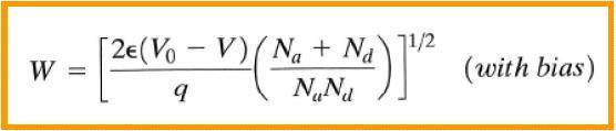
10 Space charge region, Electric Field The area under E(x) x n0 N d =x p0 N a, W=x n0 +x p0 Contact potential expressed in doping level and depletion depth
11 Space charge region, depletion depth What happened with x p0 and x n0 if N a or N d is large?
12 Current-Voltage characteristic
13 Current-Voltage Characteristic Forward biased junction: Diffusion current increase. The drift currents are almost constant
14 Current-Voltage Characteristic Reverse biased junction: Diffusion current decrease. The drift currents are almost constant
15 Current-Voltage Characteristic, forward bias junctions
16 Current-Voltage Characteristic Generation of charge carrier in the depletion region as well as charges diffuse into the junction, swept through the depletion layer by the electric field, result into a leakage current of the device

 1) Contact potential")

17 Current-Voltage Characteristic, injection of minority carrier (forward bias) 1) Contact potential caused by a different concentration across the junction 2) With bias applied 1/2 gives

18 Current-Voltage Characteristic, injection of minority carrier (forward bias) p xno = pne qv kt p xno pn = pne qv kt pn Subtracting equilibrium hole and electron conc. L Diffusion length n D n n
 Hole diffusion")

19 Current-Voltage Characteristic, injection of minority carrier (forward bias) Hole diffusion current at point x n Hole current injected into the n-material Electron current injected into the p-material

20 Current-Voltage Characteristic, the diode equation. Total current at x n =x p =0 Voltage depended minority injection included
21 Current-Voltage Characteristic, the diode equation. Reversed bias! Increasing Vr gives: Shockley Equation Good agreement for Ge. Bad for Si
22 Current-Voltage Characteristic, the diode equation. The current is constant through the component The doping affect the injection The p-doping is higher than the n-doping which gives a bigger hole injection
23 Current-Voltage Characteristic, reverse biased junction
24 Current-Voltage Characteristic, reverse biased junction
25 Current-Voltage Characteristic, 2 order effect 1. Generation and recombination in the depletion volume 2. Ohmic losses
26 Current-Voltage Characteristic, 2 order effect Thermal generation of carrier in neutral region (a) Recombination center in the bandgap. In reverse bias mode the center act as a generations center, which affect the leakage current. (b)
27 Current-Voltage Characteristic, 2 order effect The diode equation is modified to take care of the effect of recombination. An ideality factor n with a value from 1 to 2, is therefore introduced. 1 is pure diffusion and 2 is pure recombination. A real diode is somewhere in-between. I 0 is modified to better explain the current when recombination/generation center affect the leakage current. I ' 0 A q D p p n N 2 i D qnw i g Minority carrier lifetime in neutral n-doped region (p + n-diode) Generation life-time in depletion region
28 Ohmic losses V V a


29 Depletion layer capacitance Def. of Capacitance 0 V bias


30 Depletion layer capacitance Equal amount of charge on each side, opposite charge Propagation of depletion region caused by the doping Differentiation gives the junction capacitance. The capacitance is voltage dependent and decrease with increased reverse bias Can be written as a simple plate capacitor
31 Depletion layer capacitance
32 Depletion layer capacitance
33 Depletion layer capacitance s Si: K s =12

34 Diffusion capacitance Long diodes, The diode is longer than the diffusion length for the minority carrier, no contribution to the capacitance Short diodes, the most silicon diodes behave as short diodes Storage length
35 Transient Behavior Injection of minority carrier, when the diode is forward biased. p + n-diode

36 Transient Behavior After injection of carrier, the diode is reversed biased. The diode conduct until all injected carrier have recombined.
37 Junction Breakdown Zener breakdown Avalanche breakdown
38 Junction Breakdown, zener n and p are doped high, which result in tunneling through the potential barrier Negative temp. coeff Vb T

39 Junction Breakdown, Avalanche An electron is accelerated in a high electric Field, which gives impact ionization. Positive temp coeff.

40 Junction Breakdown, PIN-diode
41 Junction Breakdown, avalanche in surface
42 Junction Breakdown, avalanche in surface High Electric Field SiO p Low doped n n +
CHAPTER 8 The PN Junction Diode
 CHAPTER 8 The PN Junction Diode Consider the process by which the potential barrier of a PN junction is lowered when a forward bias voltage is applied, so holes and electrons can flow across the junction
CHAPTER 8 The PN Junction Diode
 CHAPTER 8 The PN Junction Diode Consider the process by which the potential barrier of a PN junction is lowered when a forward bias voltage is applied, so holes and electrons can flow across the junction
CHAPTER 8 The pn Junction Diode
 CHAPTER 8 The pn Junction Diode Consider the process by which the potential barrier of a pn junction is lowered when a forward bias voltage is applied, so holes and electrons can flow across the junction
Review Energy Bands Carrier Density & Mobility Carrier Transport Generation and Recombination
 Review Energy Bands Carrier Density & Mobility Carrier Transport Generation and Recombination Current Transport: Diffusion, Thermionic Emission & Tunneling For Diffusion current, the depletion layer is
Lecture 2 p-n junction Diode characteristics. By Asst. Prof Dr. Jassim K. Hmood
 Electronic I Lecture 2 p-n junction Diode characteristics By Asst. Prof Dr. Jassim K. Hmood THE p-n JUNCTION DIODE The pn junction diode is formed by fabrication of a p-type semiconductor region in intimate
EC T34 ELECTRONIC DEVICES AND CIRCUITS
 RAJIV GANDHI COLLEGE OF ENGINEERING AND TECHNOLOGY PONDY-CUDDALORE MAIN ROAD, KIRUMAMPAKKAM-PUDUCHERRY DEPARTMENT OF ECE EC T34 ELECTRONIC DEVICES AND CIRCUITS II YEAR Mr.L.ARUNJEEVA., AP/ECE 1 PN JUNCTION
NAME: Last First Signature
 UNIVERSITY OF CALIFORNIA, BERKELEY College of Engineering Department of Electrical Engineering and Computer Sciences EE 130: IC Devices Spring 2003 FINAL EXAMINATION NAME: Last First Signature STUDENT
Digital Integrated Circuits A Design Perspective. The Devices. Digital Integrated Circuits 2nd Devices
 Digital Integrated Circuits A Design Perspective The Devices The Diode The diodes are rarely explicitly used in modern integrated circuits However, a MOS transistor contains at least two reverse biased
EE/COE 152: Basic Electronics. Lecture 3. A.S Agbemenu. https://sites.google.com/site/agbemenu/courses/ee-coe-152
 EE/COE 152: Basic Electronics Lecture 3 A.S Agbemenu https://sites.google.com/site/agbemenu/courses/ee-coe-152 Books: Microelcetronic Circuit Design (Jaeger/Blalock) Microelectronic Circuits (Sedra/Smith)
10/27/2009 Reading: Chapter 10 of Hambley Basic Device Physics Handout (optional)
") EE40 Lec 17 PN Junctions Prof. Nathan Cheung 10/27/2009 Reading: Chapter 10 of Hambley Basic Device Physics Handout (optional) Slide 1 PN Junctions Semiconductor Physics of pn junctions (for reference
EE40 Lec 17 PN Junctions Prof. Nathan Cheung 10/27/2009 Reading: Chapter 10 of Hambley Basic Device Physics Handout (optional) Slide 1 PN Junctions Semiconductor Physics of pn junctions (for reference
Ch5 Diodes and Diodes Circuits
 Circuits and Analog Electronics Ch5 Diodes and Diodes Circuits 5.1 The Physical Principles of Semiconductor 5.2 Diodes 5.3 Diode Circuits 5.4 Zener Diode References: Floyd-Ch2; Gao-Ch6; 5.1 The Physical
Analog Electronic Circuits
 Analog Electronic Circuits Chapter 1: Semiconductor Diodes Objectives: To become familiar with the working principles of semiconductor diode To become familiar with the design and analysis of diode circuits
Physics 160 Lecture 5. R. Johnson April 13, 2015
 Physics 160 Lecture 5 R. Johnson April 13, 2015 Half Wave Diode Rectifiers Full Wave April 13, 2015 Physics 160 2 Note that there is no ground connection on this side of the rectifier! Output Smoothing
EC6202- ELECTRONIC DEVICES AND CIRCUITS UNIT TEST-1 EXPECTED QUESTIONS
 EC6202- ELECTRONIC DEVICES AND CIRCUITS UNIT TEST-1 EXPECTED QUESTIONS 1. List the PN diode parameters. 1. Bulk Resistance. 2. Static Resistance/Junction Resistance (or) DC Forward Resistance 3. Dynamic
Chapter 2 PN junction and diodes
 Chapter 2 PN junction and diodes ELEC-H402/CH2: PN junction and diodes 1 PN junction and diodes PN junction What happens in a PN junction Currents through the PN junction Properties of the depletion region
Electronics I. Midterm #1
 EECS:3400 Electronics I s5ms_elct7.fm - Section Electronics I Midterm # Problems Points. 4 2. 5 3. 6 Total 5 Was the exam fair? yes no EECS:3400 Electronics I s5ms_elct7.fm - 2 Problem 4 points For full
Photodiode: LECTURE-5
 LECTURE-5 Photodiode: Photodiode consists of an intrinsic semiconductor sandwiched between two heavily doped p-type and n-type semiconductors as shown in Fig. 3.2.2. Sufficient reverse voltage is applied
Key Questions ECE 340 Lecture 28 : Photodiodes
 Things you should know when you leave Key Questions ECE 340 Lecture 28 : Photodiodes Class Outline: How do the I-V characteristics change with illumination? How do solar cells operate? How do photodiodes
EDC Lecture Notes UNIT-1
 P-N Junction Diode EDC Lecture Notes Diode: A pure silicon crystal or germanium crystal is known as an intrinsic semiconductor. There are not enough free electrons and holes in an intrinsic semi-conductor
semiconductor p-n junction Potential difference across the depletion region is called the built-in potential barrier, or built-in voltage:
 Chapter four The Equilibrium pn Junction The Electric field will create a force that will stop the diffusion of carriers reaches thermal equilibrium condition Potential difference across the depletion
Department of Electrical Engineering IIT Madras
 Department of Electrical Engineering IIT Madras Sample Questions on Semiconductor Devices EE3 applicants who are interested to pursue their research in microelectronics devices area (fabrication and/or
Università degli Studi di Roma Tor Vergata Dipartimento di Ingegneria Elettronica. Analogue Electronics. Paolo Colantonio A.A.
 Università degli Studi di Roma Tor Vergata Dipartimento di Ingegneria Elettronica Analogue Electronics Paolo Colantonio A.A. 2015-16 Introduction: materials Conductors e.g. copper or aluminum have a cloud
R. W. Erickson. Department of Electrical, Computer, and Energy Engineering University of Colorado, Boulder
 R. W. Erickson Department of Electrical, Computer, and Energy Engineering University of Colorado, Boulder pn junction! Junction diode consisting of! p-doped silicon! n-doped silicon! A p-n junction where
ECE520 VLSI Design. Lecture 2: Basic MOS Physics. Payman Zarkesh-Ha
 ECE520 VLSI Design Lecture 2: Basic MOS Physics Payman Zarkesh-Ha Office: ECE Bldg. 230B Office hours: Wednesday 2:00-3:00PM or by appointment E-mail: pzarkesh@unm.edu Slide: 1 Review of Last Lecture Semiconductor
PN Junction in equilibrium
 PN Junction in equilibrium PN junctions are important for the following reasons: (i) PN junction is an important semiconductor device in itself and used in a wide variety of applications such as rectifiers,
Lecture 3: Diodes. Amplitude Modulation. Diode Detection.
 Whites, EE 322 Lecture 3 Page 1 of 10 Lecture 3: Diodes. Amplitude Modulation. Diode Detection. Diodes are the fourth basic discrete component listed in Lecture 2. These and transistors are both nonlinear
CONTENTS. 2.2 Schrodinger's Wave Equation 31. PART I Semiconductor Material Properties. 2.3 Applications of Schrodinger's Wave Equation 34
 CONTENTS Preface x Prologue Semiconductors and the Integrated Circuit xvii PART I Semiconductor Material Properties CHAPTER 1 The Crystal Structure of Solids 1 1.0 Preview 1 1.1 Semiconductor Materials
Objective Type Questions 1. Why pure semiconductors are insulators at 0 o K? 2. What is effect of temperature on barrier voltage? 3.
 Objective Type Questions 1. Why pure semiconductors are insulators at 0 o K? 2. What is effect of temperature on barrier voltage? 3. What is difference between electron and hole? 4. Why electrons have
Fundamentals of Power Semiconductor Devices
 В. Jayant Baliga Fundamentals of Power Semiconductor Devices 4y Spri ringer Contents Preface vii Chapter 1 Introduction 1 1.1 Ideal and Typical Power Switching Waveforms 3 1.2 Ideal and Typical Power Device
1) A silicon diode measures a low value of resistance with the meter leads in both positions. The trouble, if any, is
 A silicon diode measures a low value of resistance with the meter leads in both positions. The trouble, if any, is") 1) A silicon diode measures a low value of resistance with the meter leads in both positions. The trouble, if any, is A [ ]) the diode is open. B [ ]) the diode is shorted to ground. C [v]) the diode is
1) A silicon diode measures a low value of resistance with the meter leads in both positions. The trouble, if any, is A [ ]) the diode is open. B [ ]) the diode is shorted to ground. C [v]) the diode is
IENGINEERS- CONSULTANTS QUESTION BANK SERIES ELECTRONICS ENGINEERING 1 YEAR UPTU
 ELECTRONICS ENGINEERING Unit 1 Objectives Q.1 The breakdown mechanism in a lightly doped p-n junction under reverse biased condition is called. (A) avalanche breakdown. (B) zener breakdown. (C) breakdown
ELEC 3908, Physical Electronics, Lecture 16. Bipolar Transistor Operation
 ELEC 3908, Physical Electronics, Lecture 16 Bipolar Transistor Operation Lecture Outline Last lecture discussed the structure and fabrication of a double diffused bipolar transistor Now examine current
Electronics I. Midterm #1
 The University of Toledo s6ms_elct7.fm - Electronics I Midterm # Problems Points. 4 2. 5 3. 6 Total 5 Was the exam fair? yes no The University of Toledo s6ms_elct7.fm - 2 Problem 4 points For full credit,
Detectors for Optical Communications
 Optical Communications: Circuits, Systems and Devices Chapter 3: Optical Devices for Optical Communications lecturer: Dr. Ali Fotowat Ahmady Sep 2012 Sharif University of Technology 1 Photo All detectors
BASIC ELECTRONICS ENGINEERING
 BASIC ELECTRONICS ENGINEERING Objective Questions UNIT 1: DIODES AND CIRCUITS 1 2 3 4 5 6 7 8 9 10 11 12 The process by which impurities are added to a pure semiconductor is A. Diffusing B. Drift C. Doping
Electronic Circuits I. Instructor: Dr. Alaa Mahmoud
 Electronic Circuits I Instructor: Dr. Alaa Mahmoud alaa_y_emam@hotmail.com Chapter 27 Diode and diode application Outline: Semiconductor Materials The P-N Junction Diode Biasing P-N Junction Volt-Ampere
Lecture 4. pn Junctions (Diodes) Wednesday 27/9/2017 pn junctions 1-1
 Wednesday 27/9/2017 pn junctions 1-1") Lecture 4 n Junctions (Diodes) Wednesday 27/9/2017 n junctions 1-1 Agenda Continue n junctions Equilibrium (zero bias) Deletion rejoins Built-in otential Reverse and forward bias I-V characteristics Bias
Lecture 4 n Junctions (Diodes) Wednesday 27/9/2017 n junctions 1-1 Agenda Continue n junctions Equilibrium (zero bias) Deletion rejoins Built-in otential Reverse and forward bias I-V characteristics Bias
Lecture -1: p-n Junction Diode
 Lecture -1: p-n Junction Diode Diode: A pure silicon crystal or germanium crystal is known as an intrinsic semiconductor. There are not enough free electrons and holes in an intrinsic semi-conductor to
Basic Electronics Important questions
 Basic Electronics Important questions B.E-2/4 Mech- B Faculty: P.Lakshmi Prasanna Note: Read the questions in the following order i. Assignment questions ii. Class test iii. Expected questions iv. Tutorials
Lecture 9: Limiting and Clamping Diode Circuits. Voltage Doubler. Special Diode Types.
 Whites, EE 320 Lecture 9 Page 1 of 8 Lecture 9: Limiting and Clamping Diode Circuits. Voltage Doubler. Special Diode Types. We ll finish up our discussion of diodes in this lecture by consider a few more
FET(Field Effect Transistor)
") Field Effect Transistor: Construction and Characteristic of JFETs. Transfer Characteristic. CS,CD,CG amplifier and analysis of CS amplifier MOSFET (Depletion and Enhancement) Type, Transfer Characteristic,
Field Effect Transistor: Construction and Characteristic of JFETs. Transfer Characteristic. CS,CD,CG amplifier and analysis of CS amplifier MOSFET (Depletion and Enhancement) Type, Transfer Characteristic,
Lecture Course. SS Module PY4P03. Dr. P. Stamenov
 Semiconductor Devices - 2013 Lecture Course Part of SS Module PY4P03 Dr. P. Stamenov School of Physics and CRANN, Trinity College, Dublin 2, Ireland Hilary Term, TCD 01 st of Feb 13 Diode Current Components
IENGINEERS- CONSULTANTS LECTURE NOTES SERIES ELECTRONICS ENGINEERING 1 YEAR UPTU. Lecture-4
 2 P-n Lecture-4 20 Introduction: If a junction is formed between a p-type and a n-type semiconductor this combination is known as p-n junction diode and has the properties of a rectifier 21 Formation of
Section 2.3 Bipolar junction transistors - BJTs
 Section 2.3 Bipolar junction transistors - BJTs Single junction devices, such as p-n and Schottkty diodes can be used to obtain rectifying I-V characteristics, and to form electronic switching circuits
Lecture 4. Reading: Chapter EE105 Fall 2007 Lecture 4, Slide 1 Prof. Liu, UC Berkeley
 Lecture 4 OUTLNE Bipolar Junction Transistor (BJT) General considerations Structure Operation in active mode Large-signal model and - characteristics Reading: Chapter 4.1-4.4.2 EE105 Fall 2007 Lecture
Electronics The basics of semiconductor physics
 Electronics The basics of semiconductor physics Prof. Márta Rencz, Gábor Takács BME DED 17/09/2015 1 / 37 The basic properties of semiconductors Range of conductivity [Source: http://www.britannica.com]
Electronic devices-i. Difference between conductors, insulators and semiconductors
 Electronic devices-i Semiconductor Devices is one of the important and easy units in class XII CBSE Physics syllabus. It is easy to understand and learn. Generally the questions asked are simple. The unit
2 MARKS EE2203 ELECTRONIC DEVICES AND CIRCUITS UNIT 1
 2 MARKS EE2203 ELECTRONIC DEVICES AND CIRCUITS UNIT 1 1. Define PN junction. When a p type semiconductor is joined to a N type semiconductor the contact surface is called PN junction. 2. What is an ideal
UNIT 3: FIELD EFFECT TRANSISTORS
 FIELD EFFECT TRANSISTOR: UNIT 3: FIELD EFFECT TRANSISTORS The field effect transistor is a semiconductor device, which depends for its operation on the control of current by an electric field. There are
Intrinsic Semiconductor
 Semiconductors Crystalline solid materials whose resistivities are values between those of conductors and insulators. Good electrical characteristics and feasible fabrication technology are some reasons
Semiconductor Devices
 Semiconductor Devices Modelling and Technology Source Electrons Gate Holes Drain Insulator Nandita DasGupta Amitava DasGupta SEMICONDUCTOR DEVICES Modelling and Technology NANDITA DASGUPTA Professor Department
Wish you all Very Happy New Year
 Wish you all Very Happy New Year Course: Basic Electronics (EC21101) Course Instructors: Prof. Goutam Saha (Sec. 2), Prof. Shailendra K. Varshney (Sec. 1), Prof. Sudip Nag (Sec. 3 ), Prof. Debashish Sen
Part II. Devices Diode, BJT, MOSFETs
 Part II Devices Diode, BJT, MOSFETs 49 4 Semiconductor Semiconductor The number of charge carriers available to conduct current 1 is between that of conductors and that of insulators. Semiconductor is
3A.1. Lecture 3A Semiconductors. Semiconductor Structure
 3A.1 Lecture 3A Semiconductors Semiconductor structure. ptype semiconductor. ntype semiconductor. The pn junction. The pn junction characteristic (diode vi characteristic). Diode models. The Halleffect
Lesson 08. Name and affiliation of the author: Professor L B D R P Wijesundera Department of Physics, University of Kelaniya.
 Lesson 08 Title of the Experiment: Identification of active components in electronic circuits and characteristics of a Diode, Zener diode and LED (Activity number of the GCE Advanced Level practical Guide
Sub-Threshold Region Behavior of Long Channel MOSFET
 Sub-threshold Region - So far, we have discussed the MOSFET behavior in linear region and saturation region - Sub-threshold region is refer to region where Vt is less than Vt - Sub-threshold region reflects
ECE 440 Lecture 29 : Introduction to the BJT-I Class Outline:
 ECE 440 Lecture 29 : Introduction to the BJT-I Class Outline: Narrow-Base Diode BJT Fundamentals BJT Amplification Things you should know when you leave Key Questions How does the narrow-base diode multiply
Power Bipolar Junction Transistors (BJTs)
") ECE442 Power Semiconductor Devices and Integrated Circuits Power Bipolar Junction Transistors (BJTs) Zheng Yang (ERF 3017, email: yangzhen@uic.edu) Power Bipolar Junction Transistor (BJT) Background The
ECE442 Power Semiconductor Devices and Integrated Circuits Power Bipolar Junction Transistors (BJTs) Zheng Yang (ERF 3017, email: yangzhen@uic.edu) Power Bipolar Junction Transistor (BJT) Background The
Electronics I. Midterm #1
 The University of Toledo Section f6ms_elct7.fm - Electronics I Midterm # Problems Points. 4 2. 5 3. 6 Total 5 Was the exam fair? yes no The University of Toledo f6ms_elct7.fm - 2 Problem 4 points For full
SRM INSTITUTE OF SCIENCE AND TECHNOLOGY (DEEMED UNIVERSITY)
") SRM INSTITUTE OF SCIENCE AND TECHNOLOGY (DEEMED UNIVERSITY) QUESTION BANK I YEAR B.Tech (II Semester) ELECTRONIC DEVICES (COMMON FOR EC102, EE104, IC108, BM106) UNIT-I PART-A 1. What are intrinsic and
SRM INSTITUTE OF SCIENCE AND TECHNOLOGY (DEEMED UNIVERSITY) QUESTION BANK I YEAR B.Tech (II Semester) ELECTRONIC DEVICES (COMMON FOR EC102, EE104, IC108, BM106) UNIT-I PART-A 1. What are intrinsic and
QUESTION BANK EC6201 ELECTRONIC DEVICES UNIT I SEMICONDUCTOR DIODE PART A. It has two types. 1. Intrinsic semiconductor 2. Extrinsic semiconductor.
 FATIMA MICHAEL COLLEGE OF ENGINEERING & TECHNOLOGY Senkottai Village, Madurai Sivagangai Main Road, Madurai - 625 020. [An ISO 9001:2008 Certified Institution] QUESTION BANK EC6201 ELECTRONIC DEVICES SEMESTER:
Lecture Notes. Uncontrolled PSDs. Prepared by Dr. Oday A Ahmed Website: https://odayahmeduot.wordpress.com
 Lecture Notes 3 Uncontrolled PSDs Prepared by Dr. Oday A Ahmed Website: https://odayahmeduot.wordpress.com Email: 30205@uotechnology.edu.iq Scan QR Contents of this Lecture: Power Diode Characteristics
Chapter 1: Semiconductor Diodes
 Chapter 1: Semiconductor Diodes Diodes The diode is a 2-terminal device. A diode ideally conducts in only one direction. 2 Diode Characteristics Conduction Region Non-Conduction Region The voltage across
Lesson 5. Electronics: Semiconductors Doping p-n Junction Diode Half Wave and Full Wave Rectification Introduction to Transistors-
 Lesson 5 Electronics: Semiconductors Doping p-n Junction Diode Half Wave and Full Wave Rectification Introduction to Transistors- Types and Connections Semiconductors Semiconductors If there are many free
PHYSICS OF SEMICONDUCTOR DEVICES
 PHYSICS OF SEMICONDUCTOR DEVICES PHYSICS OF SEMICONDUCTOR DEVICES by J. P. Colinge Department of Electrical and Computer Engineering University of California, Davis C. A. Colinge Department of Electrical
Bipolar Junction Transistors (BJTs) Overview
 Overview") 1 Bipolar Junction Transistors (BJTs) Asst. Prof. MONTREE SIRIPRUCHYANUN, D. Eng. Dept. of Teacher Training in Electrical Engineering, Faculty of Technical Education King Mongkut s Institute of Technology
1 Bipolar Junction Transistors (BJTs) Asst. Prof. MONTREE SIRIPRUCHYANUN, D. Eng. Dept. of Teacher Training in Electrical Engineering, Faculty of Technical Education King Mongkut s Institute of Technology
Electron Devices and Circuits (EC 8353)
") Electron Devices and Circuits (EC 8353) Prepared by Ms.S.KARKUZHALI, A.P/EEE Diodes The diode is a 2-terminal device. A diode ideally conducts in only one direction. Diode Characteristics Conduction Region
Electron Devices and Circuits (EC 8353) Prepared by Ms.S.KARKUZHALI, A.P/EEE Diodes The diode is a 2-terminal device. A diode ideally conducts in only one direction. Diode Characteristics Conduction Region
KOM2751 Analog Electronics :: Dr. Muharrem Mercimek :: YTU - Control and Automation Dept. 1 1 (CONT D) DIODES
 DIODES") KOM2751 Analog Electronics :: Dr. Muharrem Mercimek :: YTU - Control and Automation Dept. 1 1 (CONT D) DIODES Most of the content is from the textbook: Electronic devices and circuit theory, Robert L.
KOM2751 Analog Electronics :: Dr. Muharrem Mercimek :: YTU - Control and Automation Dept. 1 1 (CONT D) DIODES Most of the content is from the textbook: Electronic devices and circuit theory, Robert L.
Discuss the basic structure of atoms Discuss properties of insulators, conductors, and semiconductors
 Discuss the basic structure of atoms Discuss properties of insulators, conductors, and semiconductors Discuss covalent bonding Describe the properties of both p and n type materials Discuss both forward
Digital Integrated Circuits EECS 312
 14 12 10 8 6 Fujitsu VP2000 IBM 3090S Pulsar 4 IBM 3090 IBM RY6 CDC Cyber 205 IBM 4381 IBM RY4 2 IBM 3081 Apache Fujitsu M380 IBM 370 Merced IBM 360 IBM 3033 Vacuum Pentium II(DSIP) 0 1950 1960 1970 1980
Unless otherwise specified, assume room temperature (T = 300 K).
.") ECE 3040 Dr. Doolittle Homework 4 Unless otherwise specified, assume room temperature (T = 300 K). 1) Purpose: Understanding p-n junction band diagrams. Consider a p-n junction with N A = 5x10 14 cm -3
ECE 3040 Dr. Doolittle Homework 4 Unless otherwise specified, assume room temperature (T = 300 K). 1) Purpose: Understanding p-n junction band diagrams. Consider a p-n junction with N A = 5x10 14 cm -3
P-N Diodes & Applications
 P-N Diodes & Applications Outline Major junction diode applications are Electronics circuit control Rectifying (forward mode) Special break-down diodes: Zener and avalanche Switching Circuit tuning (varactor)
ECE 3040 Dr. Alan Doolittle.
 ECE 3040 Dr. Alan Doolittle I have thoroughly enjoyed meeting each of you and hope that I have had a positive influence on your carriers. Please feel free to consult with me in your future work. If I can
Bipolar Junction Transistor (BJT) Basics- GATE Problems
 Basics- GATE Problems") Bipolar Junction Transistor (BJT) Basics- GATE Problems One Mark Questions 1. The break down voltage of a transistor with its base open is BV CEO and that with emitter open is BV CBO, then (a) BV CEO =
Bipolar Junction Transistor (BJT) Basics- GATE Problems One Mark Questions 1. The break down voltage of a transistor with its base open is BV CEO and that with emitter open is BV CBO, then (a) BV CEO =
Class XII - Physics Semiconductor Electronics. Chapter-wise Problems
 lass X - Physics Semiconductor Electronics Materials, Device and Simple ircuit hapter-wise Problems Multiple hoice Question :- 14.1 The conductivity of a semiconductor increases with increase in temperature
Analog & Digital Electronics Course No: PH-218
 Analog & Digital Electronics Course No: PH-218 Lec-5: Bipolar Junction Transistor (BJT) Course nstructors: Dr. A. P. VAJPEY Department of Physics, ndian nstitute of Technology Guwahati, ndia 1 Bipolar
EE70 - Intro. Electronics
 EE70 - Intro. Electronics Course website: ~/classes/ee70/fall05 Today s class agenda (November 28, 2005) review Serial/parallel resonant circuits Diode Field Effect Transistor (FET) f 0 = Qs = Qs = 1 2π
What is the highest efficiency Solar Cell?
 What is the highest efficiency Solar Cell? GT CRC Roof-Mounted PV System Largest single PV structure at the time of it s construction for the 1996 Olympic games Produced more than 1 billion watt hrs. of
Analog Electronics (Course Code: EE314) Lecture 5 7: Junction contd, BJT. Course Instructor: Shree Prakash Tiwari
 Lecture 5 7: Junction contd, BJT. Course Instructor: Shree Prakash Tiwari") ndian nstitute of echnology Jodhpur, Year 2017 Analog lectronics (ourse ode: 314) Lecture 5 7: Junction contd, J ourse nstructor: Shree Prakash iwari mail: sptiwari@iitj.ac.in Webpage: http://home.iitj.ac.in/~sptiwari/
ndian nstitute of echnology Jodhpur, Year 2017 Analog lectronics (ourse ode: 314) Lecture 5 7: Junction contd, J ourse nstructor: Shree Prakash iwari mail: sptiwari@iitj.ac.in Webpage: http://home.iitj.ac.in/~sptiwari/
The current density at a forward bias of 0.9 V is J( V) = 8:91 10 ;13 exp 0:06 = 9: :39=961:4 Acm ; 1: 10 ;8 exp 0:05 The current is dominated b
 = 8:91 10 ;13 exp 0:06 = 9: :39=961:4 Acm ; 1: 10 ;8 exp 0:05 The current is dominated b") Prof. Jasprit Singh Fall 000 EECS 30 Solutions to Homework 6 Problem 1 Two dierent processes are used to fabricate a Si p-n diode. The rst process results in a electron-hole recombination time via impurities
Prof. Jasprit Singh Fall 000 EECS 30 Solutions to Homework 6 Problem 1 Two dierent processes are used to fabricate a Si p-n diode. The rst process results in a electron-hole recombination time via impurities
I E I C since I B is very small
 Figure 2: Symbols and nomenclature of a (a) npn and (b) pnp transistor. The BJT consists of three regions, emitter, base, and collector. The emitter and collector are usually of one type of doping, while
Introduction to semiconductor technology
 Introduction to semiconductor technology Outline 7 Field effect transistors MOS transistor current equation" MOS transistor channel mobility Substrate bias effect 7 Bipolar transistors Introduction Minority
Semiconductor Physics and Devices
 Metal-Semiconductor and Semiconductor Heterojunctions The Metal-Oxide-Semiconductor Field-Effect Transistor (MOSFET) is one of two major types of transistors. The MOSFET is used in digital circuit, because
Lecture 7:PN Junction. Structure, Depletion region, Different bias Conditions, IV characteristics, Examples
 Lecture 7:PN Junction Structure, Depletion region, Different bias Conditions, IV characteristics, Examples PN Junction The diode (pn junction) is formed by dopping a piece of intrinsic silicon, such that
Lecture 16 - Metal-Semiconductor Junction (cont.) October 9, 2002
 October 9, 2002") 6.720J/3.43J - Integrated Microelectronic Devices - Fall 2002 Lecture 16-1 Lecture 16 - Metal-Semiconductor Junction (cont.) October 9, 2002 Contents: 1. Schottky diode 2. Ohmic contact Reading assignment:
6.720J/3.43J - Integrated Microelectronic Devices - Fall 2002 Lecture 16-1 Lecture 16 - Metal-Semiconductor Junction (cont.) October 9, 2002 Contents: 1. Schottky diode 2. Ohmic contact Reading assignment:
Semiconductor Materials and Diodes
 C C H H A A P P T T E E R R 1 Semiconductor Materials and Diodes 1.0 1.0 PREVIEW PREVIEW This text deals with the analysis and design of circuits containing electronic devices, such as diodes and transistors.
EXPERIMENT 10: SCHOTTKY DIODE CHARACTERISTICS
 EXPERIMENT 10: SCHOTTKY DIODE CHARACTERISTICS AIM: To plot forward and reverse characteristics of Schottky diode (Metal Semiconductor junction) APPARATUS: D.C. Supply (0 15 V), current limiting resistor
Field Effect Transistors (npn)
") Field Effect Transistors (npn) gate drain source FET 3 terminal device channel e - current from source to drain controlled by the electric field generated by the gate base collector emitter BJT 3 terminal
Field Effect Transistors (npn) gate drain source FET 3 terminal device channel e - current from source to drain controlled by the electric field generated by the gate base collector emitter BJT 3 terminal
LAB IV. SILICON DIODE CHARACTERISTICS
 LAB IV. SILICON DIODE CHARACTERISTICS 1. OBJECTIVE In this lab you will measure the I-V characteristics of the rectifier and Zener diodes, in both forward and reverse-bias mode, as well as learn what mechanisms
Basic Electronics. Introductory Lecture Course for. Technology and Instrumentation in Particle Physics Chicago, Illinois June 9-14, 2011
 Basic Electronics Introductory Lecture Course for Technology and Instrumentation in Particle Physics 2011 Chicago, Illinois June 9-14, 2011 Presented By Gary Drake Argonne National Laboratory Session 3
THERMIONIC AND GASEOUS STATE DIODES
 THERMIONIC AND GASEOUS STATE DIODES Thermionic and gaseous state (vacuum tube) diodes Thermionic diodes are thermionic-valve devices (also known as vacuum tubes, tubes, or valves), which are arrangements
Diode Limiters or Clipper Circuits
 Diode Limiters or Clipper Circuits Circuits which are used to clip off portions of signal voltages above or below certain levels are called limiters or clippers. Types of Clippers Positive Clipper Negative
UNIT-4. Microwave Engineering
 UNIT-4 Microwave Engineering Microwave Solid State Devices Two problems with conventional transistors at higher frequencies are: 1. Stray capacitance and inductance. - remedy is interdigital design. 2.Transit
PHYS 3050 Electronics I
 PHYS 3050 Electronics I Chapter 4. Semiconductor Diodes and Transistors Earth, Moon, Mars, and Beyond Dr. Jinjun Shan, Associate Professor of Space Engineering Department of Earth and Space Science and
Lecture - 18 Transistors
 Electronic Materials, Devices and Fabrication Dr. S. Prarasuraman Department of Metallurgical and Materials Engineering Indian Institute of Technology, Madras Lecture - 18 Transistors Last couple of classes
OPTOELECTRONIC and PHOTOVOLTAIC DEVICES
 OPTOELECTRONIC and PHOTOVOLTAIC DEVICES Outline 1. Introduction to the (semiconductor) physics: energy bands, charge carriers, semiconductors, p-n junction, materials, etc. 2. Light emitting diodes Light
Chapter 2. Diodes & Applications
 Chapter 2 Diodes & Applications The Diode A diode is made from a small piece of semiconductor material, usually silicon, in which half is doped as a p region and half is doped as an n region with a pn
Electro - Principles I
 The PN Junction Diode Introduction to the PN Junction Diode Note: In this chapter we consider conventional current flow. Page 11-1 The schematic symbol for the pn junction diode the shown in Figure 1.
Reg. No. : Question Paper Code : B.E./B.Tech. DEGREE EXAMINATION, NOVEMBER/DECEMBER Second Semester
 WK 5 Reg. No. : Question Paper Code : 27184 B.E./B.Tech. DEGREE EXAMINATION, NOVEMBER/DECEMBER 2015. Time : Three hours Second Semester Electronics and Communication Engineering EC 6201 ELECTRONIC DEVICES
SYED AMMAL ENGINEERING COLLEGE
 SYED AMMAL ENGINEERING COLLEGE (Approved by the AICTE, New Delhi, Govt. of Tamilnadu and Affiliated to Anna University, Chennai) Established in 1998 - An ISO 9001:2008 Certified Institution Dr. E.M.Abdullah