F. Hartmann. IEKP - Universität Karlsruhe (TH) IEKP - Universität Karlsruhe (TH)
|
|
|
- Eleanore Morrison
- 5 years ago
- Views:
Transcription
 and 500µm sensors after 10 years LHC Expectedpower for500 µm sensors after 10 years LHC Outlook F.")
1 Results on proton irradiation tests in Karlsruhe p do Bulk & Surface Damage Strip parameters after irrad. V FD for (300µm) and 500µm sensors after 10 years LHC Expectedpower for500 µm sensors after 10 years LHC Outlook F. Hartmann 1
 Compact Cyclotron at Forschungszentrum")
2 Irradiation Facility 34 MeV protons 1000 na Beam spot: 2cm O T < -10 C Area: 20x40cm 2 Duration: 100cm 2 in 15min (1 sensor, 5e13p/cm 2 ) Compact Cyclotron at Forschungszentrum Karlsruhe 2

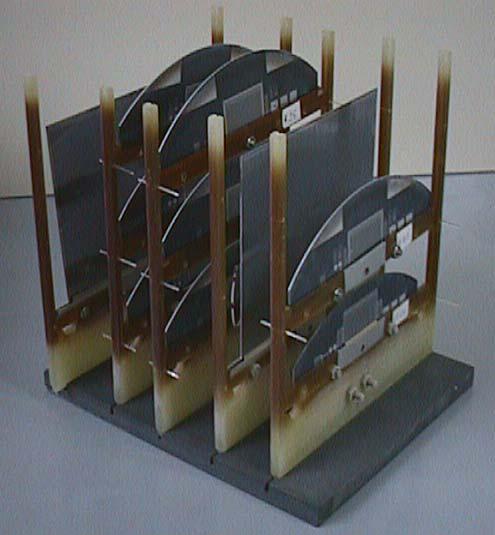
3 Cold Box Dry N 2 atmosphere at 10 C. Flexible box to hold sensors, teststructures and/or modules! Laser focus Simple power lines Temp. monitor 3
4 Simulate LHC bias conditions with respect to surface damage! During proton irrad.: Diode acts as a current source due to the p ionising effect SOLVE: 1V potential by applying V bias = 1V, But AC must also be on GND! DC diode LHC Rpoly CC AC readout (on GND) Current source Vbias Rpoly Here we need potentia like in LHC 1M Ω at 1µ A = 1V Strip current after irrad 4

 How to Realize?")
5 Simulate LHC bias conditions with respect to surface damage! Bias ring --> GND Rpoly AC DC Short all AC to bias (GND) How to Realize? Backplane to +Vbias= 1V Conductive rubber V bias = 1V during irrad 5

6 Sensors before/after Irradiation 6

7 Fluences in the Tracker ~1.5e14 n/cm 2 for 320µm Upper limits: U FD <500V P(-10 C)<400mW ~0.5e14 n/cm 2 for 500µm 7
8 Irradiation Scheme 2 fluences chosen: Inner Tracker: 1.8e14 p/cm 2 (~3e14 n/cm 2 ): expected for low resisitivity silicon (300µm) * yLHC Outer Tracker: 0.5e14 p/cm 2 (~8e13 n/cm 2 ): expected for high resistivity silicon (500µm) *1.5 15yLHC Material (6, 500µm thick): 1 sensor W6b from Hamamatsu 1 sensor OB2 from ST Microelectronics 6 teststructures from Hamamatsu Biasing: 1V, 12V, 100V, non Notice: Inner Tracker fluence on Outer Tracker (500µm) sensors instead of 300µm, PRO: 1. resistivity almost right 2. No 320µm sensors present, 3. HPK will in future deliver inner 300µm sensors CON: unusual high V FD 8
9 Fluence Measurement 1.) Measurement by Ni-foil activation behind sensors: Calibration at 26 MeV Scaling with cross section to higher energies Fluence in [p/cm2] Hardness factor κ(e) scales to neutron equivalent 2.) I leak measurement: Temperature scaling to 20 C I(20 C)=I(T)*R(T); R(T)=(293K/T) 2 e (-E/k(1/293K-1/T)) ; E=1.4eV I/V=α*Φ α(t=20 C)=4e-17 A/cm Fluence in [n(1mev)/cm 2 ] 9


10 Karlsruhe probing equipment stencil/template Bias Measurements take ~1.5-2 hours Changing of sensor ~ 5 min Environment: 10 C, RH~1% 10
11 IV-Curve before/after Irrad. 2m 2m Sensor HPK Sensor ST Sensor HPK irradiated (1.8e14 p/cm 2 ) Sensor ST irradiated (0.5e14 p/cm 2 ) Current [A] 1m 500µ 10µ 8µ 6µ 4µ 2µ Voltage [V] 11
12 Power Consumption 400.0µ 350.0µ I / V [A/cm 3 ] 300.0µ 250.0µ 200.0µ 150.0µ 100.0µ 50.0µ 0.0 Data (500µm sensors, ~5kΩcm) Linear Fit Extrapolated value for 500µm sensor at r=60cm α(t=-10 C) = A/cm P ~ U FD I ~ d 2 d ~d x x x x x x10 14 eq. Fluence [n/cm 2 ] 60µA/cm 3 => I leak (-10 C)=270µA (W6b) => P(500V, -10 C)=135mW/sensor Actual designed cooling power 400mW for each module (at least). 12
13 CV-Curve Curve before/after Irrad. 3,5x ,0x ,5x10 17 Capacitance -2 [F -2 ] 2,0x ,5x ,0x ,0x ,0 Sensor HPK Sensor ST Sensor HPK irradiated (1.8e14 p/cm 2 ) Sensor ST irradiated (0.5e14 p/cm 2 ) U FD ~ d 2 => U FD (320µm) = 410V Voltage [V] ST and HPK sensors are stable up to V bias =1000V after irradiation! Even strip tests were done at V bias = 1000V! 13
14 Hamburg Model g a τ a (20 C) c g c 2.5x10 12 U FD (N eff )~d 2 g Y τ Y (20 C) 2.0x10 12 N [cm -3 ] 1.5x x x Beneficial Annealing Stable Damage Reverse Annealing PhD Thesis M. Moll: g a =(1.81±0.14)e-2 cm -1 τ a (20 C) =55h g c =(1.49±0.04)e-2 cm -1 c=(10.9±0.8)e-2 cm -1 /N eff g Y =(5.16±0.09)e-2 cm -1 τ Y (20 C)=475d Beneficial annealing Stable Damage Reverse Annealing Time at RT [days] 14
15 Developement of U FD Full Depletion Voltage [V] Data (FS sensors) Hamburg Model ST Hamamatsu 0,0 0,5 1,0 1,5 2,0 2,5 3,0 3,5 eq. Fluence [10 14 n(1mev)/cm 2 ] Data is fully compatible with the Hamburg model fit! Predictions for different annealing scenarios possible! 15

16 Full depletion as function of annealing time and fluence Fluence given at once, then annealing. 16
17 Annealing scenario: 14 days at RT each year 600 Full Depletion Voltage [V] µm, 4.4kΩ, 5e13n/cm 2 " Fluence at once 320µm, 2.2kΩ, 16e13n/cm Annealing Time at RT [days] Iterative calculation of full depletion voltage 17
18 Depletion voltages for diode minisensor and full sensor 3,0x10 20 ~600V 2,5x10 20 Capacitance -2 [F -2 ] 2,0x ,5x ,0x ,0x10 19 Diode 2.6e14 n/cm 2 Full sensor 3e14 n/cm 2 Mini sensor 2.6e14 n/cm 2 ~600V 0, ~1000V values shifted in y for comparison to compensate for different sizes Voltage [V] Future: diode measurements as reference! 18
19 Strip Leakage Current Leakage 400V [na] Minisensor 41 Before Irradiation After Irradiation and Annealing (Measurement at -10 C) Strip number As expected: Increase in leakage current! 19
20 Bias Resistance Poly Resistance [MΩ] 2,3 2,2 2,1 2,0 1,9 1, Strip number Minisensor H41 Before Irradiation Raw Data: After Irradiation and Annealing (Measurement at -10 C) Corrected values due to high I leak Measurement: Apply U=2V Measure I Calculate R=U/I Correction: Measure I leak (high after irrad Correct R c =U/(U/R+I leak ) No change in bias resistances! 20
21 Coupling Capacitance Coupling Capacitance [pf] Strip number Minisensor H39 Before Irradiation After Irradiation and Annealing (Measurement at -10 C) No change in coupling capacitances! 21

22 Interstrip capacitance of HPK full sensor (1 neighbour) Wedgeshaped sensor: Longer strips on the sides but less neighbours! structure 100 ff 20 ff <Cint>=3.2 pf 22
23 Interstrip Capacitance Interstrip Capacitance [pf] Non irradiated: 1 MHz 100 khz Irradiated: 1 MHz 100 khz Bias Voltage [V] Interstrip Capacitance [F] (2 neighbours) 1,7p 1,7p 1,6p 1,6p 1,5p 1,5p Before Irradiation After Irradiation 1,4p Strip No. No change in interstrip capacitance before/after irrad.@ 1MH Homogeneous interstrip distribution before/after irrad. 23


24 Future CMS dedicated teststand at the Cyclotron Scan area: 20 x 50 [cm] Scan speed: 1.25x 2.5 [cm/s] Maximum load: 20kg (New dedicated beamline line) 24
 Test of components: sensor, electronics, mechanics.")
25 Future: irradiation of a full module TEC outer, TEC inner,tob,tib Longterm with high voltage, current, power Test of S/N, CCE, (pedestal,noise,shape) Test of components: sensor, electronics, mechanics. First IEKP TEC module 25
26 Conclusion 1. Both: ST and HPK comply with the specification of irradiation hardness 2. Data fits Hamburg model well and shows a decent behavior after 10 years of LHC operation 3. No changes in the strip parameters observed 4. Future dedicated teststand promise easy access to the cyclotron 5. Further plans: 300µm sensors and full modules will be irradiated! 26
27 NEW: Ingot pre-qualification (june 2001) Hamamatsu proposed to produce a couple of additional sensors out of each new ingot for irradiation pre-qualification Special procedure in addition to the standard task. All measurements on diode and minisensor Save large sensors as spares! INGOT: IV & CV on diode To determine Vdepletion, fluence estimation and α-factor PROCESS: Cint, Rint, leakage current, Rpoly vs. Vbias upto Vdepletion + 50V (for ~10 strips) 27
ATLAS Upgrade SSD. ATLAS Upgrade SSD. Specifications of Electrical Measurements on SSD. Specifications of Electrical Measurements on SSD
 ATLAS Upgrade SSD Specifications of Electrical Measurements on SSD ATLAS Project Document No: Institute Document No. Created: 17/11/2006 Page: 1 of 7 DRAFT 2.0 Modified: Rev. No.: 2 ATLAS Upgrade SSD Specifications
Silicon Sensor Developments for the CMS Tracker Upgrade
 Silicon Sensor Developments for the CMS Tracker Upgrade on behalf of the CMS tracker collaboration University of Hamburg, Germany E-mail: Joachim.Erfle@desy.de CMS started a campaign to identify the future
SSD Development for the ATLAS Upgrade Tracker
 SSD Development for the ATLAS Upgrade Tracker Meeting Mo., Feb. 26, 2007. 2-6 pm; CERN Rm. 13-3-005 ATL-P-MN-0006 v.1 Development of non-inverting Silicon strip detectors for the ATLAS ID Upgrade 1) DC
 Frank.Hartmann@CERN.CH 03.02.2012 Content & Disclaimer Different Strategies FLUKA Leakage currents Depletion Voltage Each experiment is following the same goal but with slightly different strategies An
CMS Phase II Tracker Upgrade GRK-Workshop in Bad Liebenzell
 CMS Phase II Tracker Upgrade GRK-Workshop in Bad Liebenzell Institut für Experimentelle Kernphysik KIT University of the State of Baden-Wuerttemberg and National Research Center of the Helmholtz Association
Why p-type is better than n-type? or Electric field in heavily irradiated silicon detectors
 Why p-type is better than n-type? or Electric field in heavily irradiated silicon detectors G.Kramberger, V. Cindro, I. Mandić, M. Mikuž, M. Milovanović, M. Zavrtanik Jožef Stefan Institute Ljubljana,
CMS Tracker Upgrade for HL-LHC Sensors R&D. Hadi Behnamian, IPM On behalf of CMS Tracker Collaboration
 CMS Tracker Upgrade for HL-LHC Sensors R&D Hadi Behnamian, IPM On behalf of CMS Tracker Collaboration Outline HL-LHC Tracker Upgrade: Motivations and requirements Silicon strip R&D: * Materials with Multi-Geometric
Radiation hardness and precision timing study of Silicon Detectors for the CMS High Granularity Calorimeter (HGC)
") Radiation hardness and precision timing study of Silicon Detectors for the CMS High Granularity Calorimeter (HGC) Esteban Currás1,2, Marcos Fernández2, Christian Gallrapp1, Marcello Mannelli1, Michael
Radiation hardness and precision timing study of Silicon Detectors for the CMS High Granularity Calorimeter (HGC) Esteban Currás1,2, Marcos Fernández2, Christian Gallrapp1, Marcello Mannelli1, Michael
Signal-to. to-noise with SiGe. 7 th RD50 Workshop CERN. Hartmut F.-W. Sadrozinski. SCIPP UC Santa Cruz. Signal-to-Noise, SiGe 1
 Signal-to to-noise with SiGe 7 th RD50 Workshop CERN SCIPP UC Santa Cruz Signal-to-Noise, SiGe 1 Technical (Practical) Issues The ATLAS-ID upgrade will put large constraints on power. Can we meet power
Evaluation of the Radiation Tolerance of SiGe Heterojunction Bipolar Transistors Under 24GeV Proton Exposure
 Santa Cruz Institute for Particle Physics Evaluation of the Radiation Tolerance of SiGe Heterojunction Bipolar Transistors Under 24GeV Proton Exposure, D.E. Dorfan, A. A. Grillo, M Rogers, H. F.-W. Sadrozinski,
Leakage Current Prediction for GLAST Silicon Detectors
 SCIPP 97/16 Leakage Current Prediction for GLAST Silicon Detectors T. Dubbs, H.F.-W Sadrozinski, S. Kashigan, W. Kroeger, S. Jaggar, R.Johnson, W. Rowe, A. Webster SCIPP, University of California Santa
Status of ITC-irst activities in RD50
 Status of ITC-irst activities in RD50 M. Boscardin ITC-irst, Microsystem Division Trento, Italy Outline Materials/Pad Detctors Pre-irradiated silicon INFN Padova and Institute for Nuclear Research of NASU,
irst: process development, characterization and first irradiation studies
 3D D detectors at ITC-irst irst: process development, characterization and first irradiation studies S. Ronchin a, M. Boscardin a, L. Bosisio b, V. Cindro c, G.-F. Dalla Betta d, C. Piemonte a, A. Pozza
Studies of silicon strip sensors for the ATLAS ITK project. Miguel Arratia Cavendish Laboratory, University of Cambridge
 Studies of silicon strip sensors for the ATLAS ITK project Miguel Arratia Cavendish Laboratory, University of Cambridge 1 ITK project and radiation damage Unprecedented large fluences expected for the
Quality Assurance for the ATLAS Pixel Sensor
 Quality Assurance for the ATLAS Pixel Sensor 1st Workshop on Quality Assurance Issues in Silicon Detectors J. M. Klaiber-Lodewigs (Univ. Dortmund) for the ATLAS pixel collaboration Contents: - role of
Monolithic Pixel Sensors in SOI technology R&D activities at LBNL
 Monolithic Pixel Sensors in SOI technology R&D activities at LBNL Lawrence Berkeley National Laboratory M. Battaglia, L. Glesener (UC Berkeley & LBNL), D. Bisello, P. Giubilato (LBNL & INFN Padova), P.
Monitoring of the Fabrication Process of Silicon Strip Sensors for Large Scale Productions
 SNIC Symposium, Stanford, California -- 3-6 April 26 Monitoring of the Fabrication Process of Silicon Strip Sensors for Large Scale Productions T. Bergauer Institute for High Energy Physics of the Austrian
Measurement of charge collec1on in irradiated miniature sensors for the upgrade of ATLAS Phase-II Strip tracker
 Measurement of charge collec1on in irradiated miniature sensors for the upgrade of ATLAS Phase-II Strip tracker Vladimir Cindro Jožef Stefan Institute, Ljubljana, Slovenia S.H. Abidi, A.A. Affolder, M.
Testing Silicon Detectors in the Lab
 Testing Silicon Detectors in the Lab Thomas Bergauer (HEPHY Vienna) 2 nd IPM-HEPHY detector school 15 June 2012 Schedule of my talk during 1 st detector school Semiconductor Basics (45 ) Detector concepts:
The LHCb Silicon Tracker
 Journal of Instrumentation OPEN ACCESS The LHCb Silicon Tracker To cite this article: C Elsasser 214 JINST 9 C9 View the article online for updates and enhancements. Related content - Heavy-flavour production
1. Reasons for using p-type SSD
 SCIPP 05/09 Operation of Short-Strip Silicon Detectors based on p-type Wafers in the ATLAS Upgrade ID Hartmut F.-W. Sadrozinski, Abraham Seiden SCIPP, UC Santa Cruz, CA 95064 Mara Bruzzi INFN Firenze -
Development of Double-sided Silcon microstrip Detector. D.H. Kah*, H. Park, H.J. Kim (BAERI JikLee (SNU) E. Won (Korea U)
 E. Won (Korea U)") Development of Double-sided Silcon microstrip Detector D.H. Kah*, H. Park, H.J. Kim (BAERI JikLee (SNU) E. Won (Korea U), KNU) 2005 APPI dhkah@belle.knu.ac.kr 1 1. Motivation 2. Introduction Contents 1.
Development of Double-sided Silcon microstrip Detector D.H. Kah*, H. Park, H.J. Kim (BAERI JikLee (SNU) E. Won (Korea U), KNU) 2005 APPI dhkah@belle.knu.ac.kr 1 1. Motivation 2. Introduction Contents 1.
UNIVERSITY of CALIFORNIA SANTA CRUZ
 UNIVERSITY of CALIFORNIA SANTA CRUZ CHARACTERIZATION OF THE IRST PROTOTYPE P-TYPE SILICON STRIP SENSOR A thesis submitted in partial satisfaction of the requirements for the degree of BACHELOR OF SCIENCE
Thin Silicon R&D for LC applications
 Thin Silicon R&D for LC applications D. Bortoletto Purdue University Status report Hybrid Pixel Detectors for LC Next Linear Collider:Physic requirements Vertexing 10 µ mgev σ r φ,z(ip ) 5µ m 3 / 2 p sin
Silicon Sensor and Detector Developments for the CMS Tracker Upgrade
 Silicon Sensor and Detector Developments for the CMS Tracker Upgrade Università degli Studi di Firenze and INFN Sezione di Firenze E-mail: candi@fi.infn.it CMS has started a campaign to identify the future
Pixel sensors with different pitch layouts for ATLAS Phase-II upgrade
 Pixel sensors with different pitch layouts for ATLAS Phase-II upgrade Different pitch layouts are considered for the pixel detector being designed for the ATLAS upgraded tracking system which will be operating
Evaluation of the Radiation Tolerance of Several Generations of SiGe Heterojunction Bipolar Transistors Under Radiation Exposure
 1 Evaluation of the Radiation Tolerance of Several Generations of SiGe Heterojunction Bipolar Transistors Under Radiation Exposure J. Metcalfe, D. E. Dorfan, A. A. Grillo, A. Jones, F. Martinez-McKinney,
Update of CMS Process Quality Control
 Update of CMS Process Quality Control Florence Anna Macchiolo Carlo Civinini Mirko Brianzi Strasbourg Jean-Charles Fontaine Jean-Laurent Agram Vienna Thomas Bergauer Margit Oberegger Sensor Meeting, CMS
Development of Pixel Detectors for the Inner Tracker Upgrade of the ATLAS Experiment
 Development of Pixel Detectors for the Inner Tracker Upgrade of the ATLAS Experiment Natascha Savić L. Bergbreiter, J. Breuer, A. Macchiolo, R. Nisius, S. Terzo IMPRS, Munich # 29.5.215 Franz Dinkelacker
ATLAS Upgrade SSD Project:
 ATLAS Upgrade SSD: Specifications of the ATLAS Upgrade SSD ATLAS Project Document No: Institute Document No. Created: 30/10/2006 Page: 1 of 7 DRAFT 1.0 Modified: ATLAS Upgrade SSD Project: Specifications
AIDA-2020 Advanced European Infrastructures for Detectors at Accelerators. Milestone Report
 AIDA-2020-MS15 AIDA-2020 Advanced European Infrastructures for Detectors at Accelerators Milestone Report Design specifications of test stations for irradiated silicon sensors and LHC oriented front-end
Simulation of new P-type strip detectors with trench to enhance the charge multiplication effect in the n- type electrodes
 Simulation of new P-Type strip detectors RESMDD 10, Florence 12-15.October.2010 1/15 Simulation of new P-type strip detectors with trench to enhance the charge multiplication effect in the n- type electrodes
TCAD simulations of silicon strip and pixel sensor optimization
 sensor optimization a, S. Mitsui a, S. Terada a, Y. Ikegami a, Y. Takubo a, K. Hara b, Y. Takahashi b, O. Jinnouchi c, T. Kishida c, R. Nagai c, S. Kamada d, and K. Yamamura d a KEK, Tsukuba b University
Measurements With Irradiated 3D Silicon Strip Detectors
 Measurements With Irradiated 3D Silicon Strip Detectors Michael Köhler, Michael Breindl, Karls Jakobs, Ulrich Parzefall, Liv Wiik University of Freiburg Celeste Fleta, Manuel Lozano, Giulio Pellegrini
Frequency Response Properties of the Silicon Vertex Detector for BaBar
 Frequency Response Properties of the Silicon Vertex Detector for BaBar Lawrence Lin Jeff Richman Sam Burke UCSB Summer 2001 Contents 1 Introduction 2 2 p-side of the Detector 3 3 n-side of the Detector
Strip Detectors. Principal: Silicon strip detector. Ingrid--MariaGregor,SemiconductorsasParticleDetectors. metallization (Al) p +--strips
 p +--strips") Strip Detectors First detector devices using the lithographic capabilities of microelectronics First Silicon detectors -- > strip detectors Can be found in all high energy physics experiments of the last
Strip Detectors First detector devices using the lithographic capabilities of microelectronics First Silicon detectors -- > strip detectors Can be found in all high energy physics experiments of the last
New fabrication and packaging technologies for CMOS pixel sensors: closing gap between hybrid and monolithic
 New fabrication and packaging technologies for CMOS pixel sensors: closing gap between hybrid and monolithic Outline Short history of MAPS development at IPHC Results from TowerJazz CIS test sensor Ultra-thin
CMS Beam Condition Monitoring Wim de Boer, Hannes Bol, Alexander Furgeri, Steffen Muller
 CMS Beam Condition Monitoring Wim de Boer, Hannes Bol, Alexander Furgeri, Steffen Muller BCM2 8diamonds BCM1 8diamonds each BCM2 8diamonds Beam Condition Monitoring at LHC BCM at LHC is done by about 3700
Study of the radiation-hardness of VCSEL and PIN
 Study of the radiation-hardness of VCSEL and PIN 1, W. Fernando, H.P. Kagan, R.D. Kass, H. Merritt, J.R. Moore, A. Nagarkara, D.S. Smith, M. Strang Department of Physics, The Ohio State University 191
arxiv: v3 [physics.ins-det] 9 Jan 2017
![arxiv: v3 [physics.ins-det] 9 Jan 2017](/thumbs/88/117545370.jpg "arxiv: v3 [physics.ins-det] 9 Jan 2017") Prepared for submission to JINST Topical Workshop on Electronics for Particle Physics 26-3 September 216 Karlsrhue, Germany Studies of irradiated AMS H35 CMOS detectors for the ATLAS tracker upgrade arxiv:1611.497v3
Prepared for submission to JINST Topical Workshop on Electronics for Particle Physics 26-3 September 216 Karlsrhue, Germany Studies of irradiated AMS H35 CMOS detectors for the ATLAS tracker upgrade arxiv:1611.497v3
PoS(EPS-HEP 2009)150. Silicon Detectors for the slhc - an Overview of Recent RD50 Results. Giulio Pellegrini 1. On behalf of CERN RD50 collaboration
150. Silicon Detectors for the slhc - an Overview of Recent RD50 Results. Giulio Pellegrini 1. On behalf of CERN RD50 collaboration") Silicon Detectors for the slhc - an Overview of Recent RD50 Results 1 Centro Nacional de Microelectronica CNM- IMB-CSIC, Barcelona Spain E-mail: giulio.pellegrini@imb-cnm.csic.es On behalf of CERN RD50
Silicon Detectors for the slhc - an Overview of Recent RD50 Results 1 Centro Nacional de Microelectronica CNM- IMB-CSIC, Barcelona Spain E-mail: giulio.pellegrini@imb-cnm.csic.es On behalf of CERN RD50
Radiation-hard/high-speed data transmission using optical links
 Radiation-hard/high-speed data transmission using optical links K.K. Gan a, B. Abi c, W. Fernando a, H.P. Kagan a, R.D. Kass a, M.R.M. Lebbai b, J.R. Moore a, F. Rizatdinova c, P.L. Skubic b, D.S. Smith
AVALANCHE PHOTODIODES FOR THE CMS ELECTROMAGNETIC CALORIMETER
 AVALANCHE PHOTODIODES FOR THE CMS ELECTROMAGNETIC CALORIMETER B. Patel, R. Rusack, P. Vikas(email:Pratibha.Vikas@cern.ch) University of Minnesota, Minneapolis, U.S.A. Y. Musienko, S. Nicol, S.Reucroft,
Description and Evaluation of Multi-Geometry Silicon Prototype Sensors for the LHCb Inner Tracker
 LHCb Note 22-38 Description and Evaluation of Multi-Geometry Silicon Prototype Sensors for the LHCb Inner Tracker F. Lehner, P. Sievers, O. Steinkamp, U. Straumann, A. Vollhardt, M. Ziegler Physik-Institut
Dual operational amplifier
 DESCRIPTION The 77 is a pair of high-performance monolithic operational amplifiers constructed on a single silicon chip. High common-mode voltage range and absence of latch-up make the 77 ideal for use
The upgrade of the ATLAS silicon strip tracker
 On behalf of the ATLAS Collaboration IFIC - Instituto de Fisica Corpuscular (University of Valencia and CSIC), Edificio Institutos de Investigacion, Apartado de Correos 22085, E-46071 Valencia, Spain E-mail:
A High-Granularity Timing Detector for the Phase-II upgrade of the ATLAS Calorimeter system Detector concept description and first beam test results
 A High-Granularity Timing Detector for the Phase-II upgrade of the ATLAS Calorimeter system Detector concept description and first beam test results 03/10/2017 ATL-LARG-SLIDE-2017-858 Didier Lacour On
Review of Silicon Inner Tracker
 Review of Silicon Inner Tracker H.J.Kim (KyungPook National U.) Talk Outline Configuration optimization of BIT and FIT Silicon Sensor R&D Electronics R&D Summary and Plan Detail study will be presented
The CMS Silicon Strip Tracker and its Electronic Readout
 The CMS Silicon Strip Tracker and its Electronic Readout Markus Friedl Dissertation May 2001 M. Friedl The CMS Silicon Strip Tracker and its Electronic Readout 2 Introduction LHC Large Hadron Collider:
The LHCb VELO Upgrade. Stefano de Capua on behalf of the LHCb VELO group
 The LHCb VELO Upgrade Stefano de Capua on behalf of the LHCb VELO group Overview [J. Instrum. 3 (2008) S08005] LHCb / Current VELO / VELO Upgrade Posters M. Artuso: The Silicon Micro-strip Upstream Tracker
The BaBar Silicon Vertex Tracker (SVT) Claudio Campagnari University of California Santa Barbara
 Claudio Campagnari University of California Santa Barbara") The BaBar Silicon Vertex Tracker (SVT) Claudio Campagnari University of California Santa Barbara Outline Requirements Detector Description Performance Radiation SVT Design Requirements and Constraints
The BaBar Silicon Vertex Tracker (SVT) Claudio Campagnari University of California Santa Barbara Outline Requirements Detector Description Performance Radiation SVT Design Requirements and Constraints
Geiger-mode APDs (2)
") (2) Masashi Yokoyama Department of Physics, University of Tokyo Nov.30-Dec.4, 2009, INFN/LNF Plan for today 1. Basic performance (cont.) Dark noise, cross-talk, afterpulsing 2. Radiation damage 2 Parameters
(2) Masashi Yokoyama Department of Physics, University of Tokyo Nov.30-Dec.4, 2009, INFN/LNF Plan for today 1. Basic performance (cont.) Dark noise, cross-talk, afterpulsing 2. Radiation damage 2 Parameters
UV/EUV CONTINUOUS POSITION SENSOR
 UV/EUV CONTINUOUS POSITION SENSOR ODD-SXUV-DLPSD FEATURES Submicron position resolution Stable response after exposure to UV/EUV 5 mm x 5 mm active area TO-8 windowless package RoHS ELECTRO-OPTICAL CHARACTERISTICS
A High-Granularity Timing Detector for the Phase-II upgrade of the ATLAS Detector system
 A High-Granularity Timing Detector for the Phase-II upgrade of the ATLAS Detector system C.Agapopoulou on behalf of the ATLAS Lar -HGTD group 2017 IEEE Nuclear Science Symposium and Medical Imaging Conference
FACTOR: first results on SiPM characterization
 FACTOR: first results on SiPM characterization Valter Bonvicini INFN Trieste OUTLINE: 1. Motivations and program of the FACTOR project 2. Types of devices tested, measurements performed and set-up used
OPTICAL LINK OF THE ATLAS PIXEL DETECTOR
 OPTICAL LINK OF THE ATLAS PIXEL DETECTOR K.K. Gan, W. Fernando, P.D. Jackson, M. Johnson, H. Kagan, A. Rahimi, R. Kass, S. Smith Department of Physics, The Ohio State University, Columbus, OH 43210, USA
Department of Physics & Astronomy
 Department of Physics & Astronomy Experimental Particle Physics Group Kelvin Building, University of Glasgow, Glasgow, G12 8QQ, Scotland Telephone: +44 (0)141 339 8855 Fax: +44 (0)141 330 5881 GLAS-PPE/2005-14
THE SILICON SENSOR FOR THE COMPACT MUON SOLENOID CONTROL OF THE FABRICATION PROCESS
 THE SILICON SENSOR FOR THE COMPACT MUON SOLENOID CONTROL OF THE FABRICATION PROCESS F. MANOLESCU 1, A. MACCHIOLO 2, M. BRIANZI 2, A. MIHUL 3 1 Institute of Space Sciences, Magurele, Bucharest, Romania
Low Power Sensor Concepts
 Low Power Sensor Concepts Konstantin Stefanov 11 February 2015 Introduction The Silicon Pixel Tracker (SPT): The main driver is low detector mass Low mass is enabled by low detector power Benefits the
MICROELECTRONIC CIRCUIT DESIGN Third Edition
 MICROELECTRONIC CIRCUIT DESIGN Third Edition Richard C. Jaeger and Travis N. Blalock Answers to Selected Problems Updated 1/25/08 Chapter 1 1.3 1.52 years, 5.06 years 1.5 1.95 years, 6.46 years 1.8 113
Study of irradiated 3D detectors. University of Glasgow, Scotland. University of Glasgow, Scotland
 Department of Physics & Astronomy Experimental Particle Physics Group Kelvin Building, University of Glasgow Glasgow, G12 8QQ, Scotland Telephone: ++44 (0)141 339 8855 Fax: +44 (0)141 330 5881 GLAS-PPE/2002-20
ATLAS strip detector upgrade for the HL-LHC
 ATL-INDET-PROC-2015-010 26 August 2015, On behalf of the ATLAS collaboration Santa Cruz Institute for Particle Physics, University of California, Santa Cruz E-mail: zhijun.liang@cern.ch Beginning in 2024,
Sensor production readiness
 Sensor production readiness G. Bolla, Purdue University for the USCMS FPIX group PMG review 02/25/2005 2/23/2005 1 Outline Sensor requirements Geometry Radiation hardness Development Guard Rings P stops
Development of a large area silicon pad detector for the identification of cosmic ions
 Development of a large area silicon pad detector for the identification of cosmic ions M.Y. Kim 1,2 P.S. Marrocchesi 1, C. Avanzini 2, M.G. Bagliesi 1, G. Bigongiari 1,A. Caldarone 1,R. Cecchi 1,, P. Maestro
PoS(VERTEX2015)008. The LHCb VELO upgrade. Sophie Elizabeth Richards. University of Bristol
008. The LHCb VELO upgrade. Sophie Elizabeth Richards. University of Bristol") University of Bristol E-mail: sophie.richards@bristol.ac.uk The upgrade of the LHCb experiment is planned for beginning of 2019 unitl the end of 2020. It will transform the experiment to a trigger-less
University of Bristol E-mail: sophie.richards@bristol.ac.uk The upgrade of the LHCb experiment is planned for beginning of 2019 unitl the end of 2020. It will transform the experiment to a trigger-less
The HGTD: A SOI Power Diode for Timing Detection Applications
 The HGTD: A SOI Power Diode for Timing Detection Applications Work done in the framework of RD50 Collaboration (CERN) M. Carulla, D. Flores, S. Hidalgo, D. Quirion, G. Pellegrini IMB-CNM (CSIC), Spain
Unless otherwise specified, assume room temperature (T = 300 K).
.") ECE 3040 Dr. Doolittle Homework 4 Unless otherwise specified, assume room temperature (T = 300 K). 1) Purpose: Understanding p-n junction band diagrams. Consider a p-n junction with N A = 5x10 14 cm -3
ECE 3040 Dr. Doolittle Homework 4 Unless otherwise specified, assume room temperature (T = 300 K). 1) Purpose: Understanding p-n junction band diagrams. Consider a p-n junction with N A = 5x10 14 cm -3
Status of ATLAS & CMS Experiments
 Status of ATLAS & CMS Experiments Atlas S.C. Magnet system Large Air-Core Toroids for µ Tracking 2Tesla Solenoid for inner Tracking (7*2.5m) ECAL & HCAL outside Solenoid Solenoid integrated in ECAL Barrel
Sensor Concepts for Pixel Detectors in HEP
 Introduction "p in n" Sensors design, te, limits in radiation hardness "n in n" Sensors for LHC Experiments radiation hardness requirements n side isolation and design Other Experiments "Super LHC" TESLA
Experiment 9 Bipolar Junction Transistor Characteristics
 Experiment 9 Bipolar Junction Transistor Characteristics W.T. Yeung, W.Y. Leung, and R.T. Howe UC Berkeley EE 105 Fall 2005 1.0 Objective In this lab, you will determine the I C - V CE characteristics
Gamma-ray Large Area Space Telescope (GLAST) Large Area Telescope (LAT) Silicon Detector Specification
 Large Area Telescope (LAT) Silicon Detector Specification") GLAST LAT PROCUREMENT SPECIFICATION Document # Document Title GLAST LAT Silicon Detector Specification Date Effective Page 1 of 21 GE-00011-A 1rst Draft 8/20/00 Author(s) Supersedes H. Sadrozinski T. Ohsugi
GLAST LAT PROCUREMENT SPECIFICATION Document # Document Title GLAST LAT Silicon Detector Specification Date Effective Page 1 of 21 GE-00011-A 1rst Draft 8/20/00 Author(s) Supersedes H. Sadrozinski T. Ohsugi
Lecture 2. Part 2 (Semiconductor detectors =sensors + electronics) Segmented detectors with pn-junction. Strip/pixel detectors
 Segmented detectors with pn-junction. Strip/pixel detectors") Lecture 2 Part 1 (Electronics) Signal formation Readout electronics Noise Part 2 (Semiconductor detectors =sensors + electronics) Segmented detectors with pn-junction Strip/pixel detectors Drift detectors
Lecture 2 Part 1 (Electronics) Signal formation Readout electronics Noise Part 2 (Semiconductor detectors =sensors + electronics) Segmented detectors with pn-junction Strip/pixel detectors Drift detectors
The CMS Pixel Detector Upgrade and R&D Developments for the High Luminosity LHC
 The CMS Pixel Detector Upgrade and R&D Developments for the High Luminosity LHC On behalf of the CMS Collaboration INFN Florence (Italy) 11th 15th September 2017 Las Caldas, Asturias (Spain) High Luminosity
Simulation of High Resistivity (CMOS) Pixels
 Pixels") Simulation of High Resistivity (CMOS) Pixels Stefan Lauxtermann, Kadri Vural Sensor Creations Inc. AIDA-2020 CMOS Simulation Workshop May 13 th 2016 OUTLINE 1. Definition of High Resistivity Pixel Also
Simulation of High Resistivity (CMOS) Pixels Stefan Lauxtermann, Kadri Vural Sensor Creations Inc. AIDA-2020 CMOS Simulation Workshop May 13 th 2016 OUTLINE 1. Definition of High Resistivity Pixel Also
Department of Electrical Engineering IIT Madras
 Department of Electrical Engineering IIT Madras Sample Questions on Semiconductor Devices EE3 applicants who are interested to pursue their research in microelectronics devices area (fabrication and/or
Standard InGaAs Photodiodes IG17-Series
 Description The IG17-series is a panchromatic PIN photodiode with a nominal wavelength cut-off at 1.7 µm. This series has been designed for demanding spectroscopic and radiometric applications. It offers
CMS Tracker Upgrades. R&D Plans, Present Status and Perspectives. Benedikt Vormwald Hamburg University on behalf of the CMS collaboration
 R&D Plans, Present Status and Perspectives Benedikt Vormwald Hamburg University on behalf of the CMS collaboration EPS-HEP 2015 Vienna, 22.-29.07.2015 CMS Tracker Upgrade Program LHC HL-LHC ECM[TeV] 7-8
Prototype Performance and Design of the ATLAS Pixel Sensor
 Prototype Performance and Design of the ATLAS Pixel Sensor F. Hügging, for the ATLAS Pixel Collaboration Contents: - Introduction - Sensor Concept - Performance fi before and after irradiation - Conclusion
Silicon Sensors for High-Luminosity Trackers - RD50 Collaboration status report
 Silicon Sensors for High-Luminosity Trackers - RD50 Collaboration status report Albert-Ludwigs-Universität Freiburg (DE) E-mail: susanne.kuehn@cern.ch The revised schedule for the Large Hadron Collider
STUDY OF THE RADIATION HARDNESS OF VCSEL AND PIN ARRAYS
 STUDY OF THE RADIATION HARDNESS OF VCSEL AND PIN ARRAYS K.K. GAN, W. FERNANDO, H.P. KAGAN, R.D. KASS, A. LAW, A. RAU, D.S. SMITH Department of Physics, The Ohio State University, Columbus, OH 43210, USA
VELO: the LHCb Vertex Detector
 LHCb note 2002-026 VELO VELO: the LHCb Vertex Detector J. Libby on behalf of the LHCb collaboration CERN, Meyrin, Geneva 23, CH-1211, Switzerland Abstract The Vertex Locator (VELO) of the LHCb experiment
The Compact Muon Solenoid Experiment. Conference Report. Mailing address: CMS CERN, CH-1211 GENEVA 23, Switzerland
 Available on CMS information server CMS CR -2015/213 The Compact Muon Solenoid Experiment Conference Report Mailing address: CMS CERN, CH-1211 GENEVA 23, Switzerland 05 October 2015 (v2, 12 October 2015)
Tracking Detectors for the LHC Upgrade
 Tracking Detectors for the LHC Upgrade Layout Signal Noise Hartmut F.-W. Sadrozinski SCIPP, UC Santa Cruz 1 slhc, the Machine Albert De Roeck CERN 626 Upgrade in 3 main Phases: Phase 0 maximum performance
First Results with the Prototype Detectors of the Si/W ECAL
 First Results with the Prototype Detectors of the Si/W ECAL David Strom University of Oregon Physics Design Requirements Detector Concept Silicon Detectors - Capacitance and Trace Resistance Implications
IV curves of different pixel cells
 IV curves of different pixel cells 6 5 100 µm pitch, 10µm gap 100 µm pitch, 50µm gap current [pa] 4 3 2 1 interface generation current volume generation current 0 0 50 100 150 200 250 bias voltage [V]
Development of Monolithic CMOS Pixel Sensors for the ILC at LBNL
 SNIC Symposium, Stanford, California -- 3-6 April 6 Development of Monolithic CMOS Pixel Sensors for the ILC at LBNL M. Battaglia, B. Hooberman, L. Tompkins Department of Physics, University of California,
Initial Results from a Cryogenic Proton Irradiation of a p-channel CCD
 Centre for Electronic Imaging Initial Results from a Cryogenic Proton Irradiation of a p-channel CCD Jason Gow Daniel Wood, David Hall, Ben Dryer, Simeon Barber, Andrew Holland and Neil Murray Jason P.
Silicon Avalanche Photodiode SAR-/SARP-Series
 Silicon Avalanche Photodiode SAR-/SARP-Series DESCRIPTION The SAR500-Series is based on a reach-through structure for excellent quantum efficiency and high speed. The peak sensitivity in the NIR region
Resolution studies on silicon strip sensors with fine pitch
 Resolution studies on silicon strip sensors with fine pitch Stephan Hänsel This work is performed within the SiLC R&D collaboration. LCWS 2008 Purpose of the Study Evaluate the best strip geometry of silicon
HV BOARD. Claudio Arnaboldi Gianluigi Pessina INFN, Milano. Thierry Gys, Didier Piedigrossi CERN. LHCb, 15/12/2004 1
 HV BOARD Claudio Arnaboldi Gianluigi Pessina INFN, Milano Thierry Gys, Didier Piedigrossi CERN LHCb, 15/12/2004 1 HV distribution Half Column (8 HPDs) Half Column (8 HPDs) 20 KV Input HPD 2 HPD 1 FILTER
A GSM Band Low-Power LNA 1. LNA Schematic
 A GSM Band Low-Power LNA 1. LNA Schematic Fig1.1 Schematic of the Designed LNA 2. Design Summary Specification Required Simulation Results Peak S21 (Gain) > 10dB >11 db 3dB Bandwidth > 200MHz (
Pin photodiode Quality Assurance Procedure
 GENEVE, SUISSE GENEVA, SWITZERLAND ORGANISATION EUROPEENE POUR LA RECHERCHE NUCLEAIRE EUROPEAN ORGANIZATION FOR NUCLEAR RESEARCH Laboratoire Européen pour la Physique des Particules European Laboratory
Results of FE65-P2 Pixel Readout Test Chip for High Luminosity LHC Upgrades
 for High Luminosity LHC Upgrades R. Carney, K. Dunne, *, D. Gnani, T. Heim, V. Wallangen Lawrence Berkeley National Lab., Berkeley, USA e-mail: mgarcia-sciveres@lbl.gov A. Mekkaoui Fermilab, Batavia, USA
CMS Silicon Strip Tracker: Operation and Performance
 CMS Silicon Strip Tracker: Operation and Performance Laura Borrello Purdue University, Indiana, USA on behalf of the CMS Collaboration Outline The CMS Silicon Strip Tracker (SST) SST performance during
Layout and prototyping of the new ATLAS Inner Tracker for the High Luminosity LHC
 Layout and prototyping of the new ATLAS Inner Tracker for the High Luminosity LHC Ankush Mitra, University of Warwick, UK on behalf of the ATLAS ITk Collaboration PSD11 : The 11th International Conference
First Sensor Evaluation Board Data Sheet Part Description MOD Order #
 FOTO Input + 5 DC voltage Optical input (optional C-mount for lens) Mechanical potentiometer for APD-bias setting Output 16 channels voltage signal of amplified APD (300 MHz bandwidth and additional gain
Preparing for the Future: Upgrades of the CMS Pixel Detector
 : KSETA Plenary Workshop, Durbach, KIT Die Forschungsuniversität in der Helmholtz-Gemeinschaft www.kit.edu Large Hadron Collider at CERN Since 2015: proton proton collisions @ 13 TeV Four experiments:
Paper-1 (Circuit Analysis) UNIT-I
 UNIT-I") Paper-1 (Circuit Analysis) UNIT-I AC Fundamentals & Kirchhoff s Current and Voltage Laws 1. Explain how a sinusoidal signal can be generated and give the significance of each term in the equation? 2. Define
Paper-1 (Circuit Analysis) UNIT-I AC Fundamentals & Kirchhoff s Current and Voltage Laws 1. Explain how a sinusoidal signal can be generated and give the significance of each term in the equation? 2. Define
problem grade total
 Fall 2005 6.012 Microelectronic Devices and Circuits Prof. J. A. del Alamo Name: Recitation: November 16, 2005 Quiz #2 problem grade 1 2 3 4 total General guidelines (please read carefully before starting):
Silicon Sensors for HL LHC Tracking Detectors
 Silicon Sensors for HL LHC Tracking Detectors N25: Radiation Damage Effects 31. October 2012 Susanne Kuehn University of Freiburg, Germany On behalf of the RD50 Collaboration Outline Introduction Research