Department of Electrical and Information Engineering. Electronic Research Group
|
|
|
- Vernon Horn
- 5 years ago
- Views:
Transcription


1 University of Cassino and southern Lazio Department of Electrical and Information Engineering Electronic Research Group Laboratory of Industrial Electronics Contact: prof. Giovanni Busatto
2 ELECTRONICS Group STAFF Laboratory of Industrial Electronics Department of Electrical and Information Engineering Full Professor: Giovanni Busatto Associate Professors: Francesco Iannuzzo Annunziata Sanseverino Researchers: Francesco Velardi Carmine Abbate Ph.D. Student: Valentina De Luca Laboratory Technician: Tomasino Iovini
3 Main Activities Experimental (NDT) characterization of Power Devices Overvoltage, overcurrent, high and low temperature, short circuit stresses on power devices and modules Cosmic Ray effects on Power Devices (Burnout & Total dose) 2D/3D Devices FEM Simulation Devices Modeling & Simulation Lumped-Charge approach High-Voltage/high-current/picoampere PCB layout design
4 Recent Active collaborations ANSALDOBREDA Naples Italy STMicroelectronics Catania Italy Fairchild Munich Germany ECPE European Centre for Power Electronics Nuremberg - Germany INFN Italian Institute for Nuclear Physics Rome - Italy

5 The laboratory is an ECPE Competence Center specialized in non destructive testing of discrete and power modules

 Current: 0-8000A")

6 Non-Destructive Tester NDT Facility Tester control panel Features: High voltage Area Voltage: V (8000V) Current: A Applications: SOA Tests Sort circuit Unclamped Temperature Aging Principle Schematic


7 High Voltage NDT High voltage Devices: 1700V Vcc 6500V Ls = 110 nh Cs = 5nF
8 High Current NDT High current Devices: Ic 8000A Vcc 1700V Ls < 50 nh Cs = 12nF


9 Very Low Inductance NDT Very Fast Devices: Vcc 1700V, Ls < 30 nh, Cs < 300pF Detail of busbar


10 Temperature Characterization Railway inverter under test -50 C +200 C Special Fluid


 Keithley")

11 Static Characterization Curve Tracer kV, 20A pulsed Agilent B1500A w/ 2 SMUs: High current and voltage junction BV High precision (pa) oxides percolation Ad hoc set-ups: high voltage and current, high precision (e.g. 3kV 1nA) Keithley Measurement System w/2 SMUs: High current and voltage 2410 High precision (pa) 2601


12 Post Failure Analysis Inspection microscope NISENE decapsulation system


13 Development of high voltage, high performances switch Marx modulator High voltage bridge leg For railway applications


14 Cosmic Ray effects on Power Devices

15 Single Event Burnout: Experiment

16 3-µm resolution Ion Impact Mapping
17
18 Operations of power devices in highly stressing electrical conditions C. Abbate, G. Busatto, F.Iannuzzo DIEI Università di Cassino e del Lazio Meridionale Via G. di Biasio, 43, Cassino, Italy busatto@unicas.it
19 Outline Introduction Failure mechanisms under extreme electrical stresses: In the device linear operating region During the device switching In avalanche conditions External causes (eg. cosmic rays impacts) Non destructive techniques for electrical testing of power devices The basics of ND techniques taken from the literature The approach to ND SOA characterization of power module Typical problems related with the use of Non Destructive tester The precursors of the instabilities Cosmic rays impact Conclusions


20 A power device in a switching circuit Buck converter Test circuit Switch On Off
21 Switching Waveforms

22 Electrical limits of a power semiconductor switch Collector Voltage SOA Collector Voltage


23 Elementary cells of a Power MOSFET Double Diffused Planar Structure Trench Gate Structure
24 Power MOSFET parasitic BJT Source Emitter Gate Body Base N + P _ R P+ P + N _ A possible cause of failure! N + Drain Collector
25 IGBT (Insulated Gate Bipolar Transistor) Planar Structure Trench Gate Structure


26 IGBT (Insulated Gate Bipolar Transistor) Planar Structure Trench Gate Structure


27 IGBT parasitic thyristor A further possible cause of failure!
28 Outline Introduction Failure mechanisms under extreme electrical stresses: In the device linear operating region During the device switching In avalanche conditions External causes (eg. cosmic rays impacts) Non destructive techniques for electrical testing of power devices The basics of ND techniques taken from the literature The approach to ND SOA characterization of power module Typical problems related with the use of Non Destructive tester The precursors of the instabilities Cosmic rays impact Conclusions
29 Failure mechanisms under extreme electrical stresses In the device linear operating region Short circuit operations (or overload conditions) Instable DC operations (second breakdown) During the device switching At the turn-off Reverse recovery of internal diode In avalanche conditions UIS Unclamped Inductive Switch
30 Type 1 Short circuit of a Power Switch: Definitions Type 1: Short circuit takes place when the device is in the off-state so it is turned on in short circuit Type 2: Short circuit takes place when the device is in the on-state Type 2

31 Type 1 short circuit Vgs Commercial devices can sustain S.C. for 10 ms at the T JMAX and with V GS =16V

32 The failure of a Power MOSFET after a short circuit Fresh Device After a short circuit Failure
33 Type 1 short circuit: First failure mechanism A.Ammous, K.Ammous, H.Morel, B.Allard, D. Bergogne, F. Sellami, J.P.Chante Electrothermal Modeling of IGBT s: Application to Short-Circuit Conditions, IEEE Trans. Power Electronics, Vol. 15, No. 4, JULY 2000
34 Type 1 short circuit: Second failure mechanism Device avalanching due to stray inductance
35 Type 2 short circuit Avalanche limit S.C. Device avalanching due to stray inductance can cause device failure H.G.Eckel, L.Sack, Experimental Investigation on the Behaviour of IGBT at Short-Ciruit during the On-State, Proc. IEEE PESC, 1995
36 Failure mechanisms under extreme electrical stresses In the device linear operating region Short circuit operations (or overload conditions) Instable DC operations (second breakdown) During the device switching At the turn-off Reverse recovery of internal diode In avalanche conditions UIS Unclamped Inductive Switch

37 Failure of Power Devices in the active region DC Safe Operating Area Second Breakdown

38 DC electro-thermal instability of a low voltage Power MOSFET Evolution of the temperature in the hot-spot P.Spirito, G.Breglio, V.d'Alessandro, N.Rinaldi, Analytical Model for Thermal Instability of Low Voltage Power MOS and S.O.A. in Pulse Operation, Proc. ISPSD 2002
39 Basic mechanism in thermal run-away Generated Power vs. Temperature I D Regenerative Thermo-electric Effect I D a T <0 Stable a T >0 Unstable
40 Trans-characteristics of a low voltage Power MOSFET V GS =Const a T I D T 0 Possible thermal run-away P.Spirito, G.Breglio, V.d Alessandro, Modeling the Onset of Thermal Instability in Low Voltage Power MOS: an Experimental Validation, Proc. ISPSD 2005

41 Experimental evidence of hot-spot formation Radiometric temperature detection for 55V Power MOSFET operated under pulsed bias conditions P.Spirito, G.Breglio, V.d Alessandro, Modeling the Onset of Thermal Instability in Low Voltage Power MOS: an Experimental Validation, Proc. ISPSD 2005
42 Failure mechanisms under extreme electrical stresses In the device linear operating region Short circuit operations (or overload conditions) Instable DC operations (second breakdown) During the device switching At the turn-off Reverse recovery of internal diode In avalanche conditions UIS Unclamped Inductive Switch
43 Second Breakdown in a BJT


44 3D structure of a Power BJT Typical top layout of a power BJT Sketch of the 3D structure of a power BJT
45 Crowding of emitter current Reverse Base Bias: central current crowding B.A.Betty, S. Krishna, M.S.Adler, Second Breakdown in Power Transistors Due to Avalanche Injection Trans. Electron Devices, Vol.ED-23, No.8, 1976
46 Second Breakdown in a BJT Avalanche injection Impact ionizzation At increasing Drain current
47 Second Breakdown in IGBT IGBT Modules rated at 3300V-1200A Vcc=1800V, Ic=4000A R ON =R OFF =0.35Ω L load =100µH T=145 C Second breakdown along the voltage rise

48 Internal structure of a power IGBT module I G1 I C1
49 Failure mechanisms under extreme electrical stresses In the device linear operating region Short circuit operations (or overload conditions) Instable DC operations (second breakdown) During the device switching At the turn-off Reverse recovery of internal diode In avalanche conditions UIS Unclamped Inductive Switch
50 Reverse Recovery of Power MOSFET internal diode Test circuito Experimental waveforms Second Breakdown
51 Parassitic BJT Activation Source Emitter Gate Body Base N + R P+ P + P _ Supplemental Charge N _ N + Drain Collector


52 The role of gate capacitance in the activation of parasitic BJT Displacement current
53 Phenomenon insight Displacem ent current 53
54 Failure mechanisms under extreme electrical stresses In the device linear operating region Short circuit operations (or overload conditions) Instable DC operations (second breakdown) During the device switching At the turn-off Reverse recovery of internal diode In avalanche conditions UIS Unclamped Inductive Switch
55 UIS Typical waveforms
56 Safe Unclamped Inductive Switch Test circuit Typical waveforms

57 Failure of Power MOSFET in Unclamped Inductive Switch UIS Failure Waveforms The gate is Off The current Is still flowing The voltage suddenly falls down A. Icaza-Deckelmann, G. Wachutka, J. Krumrey, F. Hirler, Failure Mechanism of Power DMOS Transistors under UIS Stress Conditions, ASDAM EDSSC 03

58 Failure of Power MOSFET in Unclamped Inductive Switch Low Drain Current Electric Field I h I h I e Avalanche multiplication I e
59 Failure of Power MOSFET in Unclamped Inductive Switch I e I h Maximum temperature in the device and currents at the source contact vs. time (I=1mA)

60 Failure of Power MOSFET in Unclamped Inductive Switch High Drain Current Electric Field I e I h Kirk Effect Avalanche multiplication


61 Experimental evidence of instability in UIS
62 Outline Introduction Failure mechanisms under extreme electrical stresses: In the device linear operating region During the device switching In avalanche conditions External causes (eg. cosmic rays impacts) Non destructive techniques for electrical testing of power devices Motivation of ND techniques The basics of ND techniques taken from the literature The approach to ND SOA characterization of power module Typical problems related with the use of Non Destructive tester The precursors of the instabilities Cosmic rays impact Conclusions
63 ND techniques for electrical testing of power devices Motivation of ND techniques The basics of ND techniques taken from the literature The approach to ND SOA characterization of power module Typical problems related with the use of Non Destructive tester The precursors of the instabilities
64 How a Non-Destructive tester can help in robustness validation tests? Collector Voltage RBSOA Collector Voltage
65 How a Non-Destructive tester can help in robustness validation tests? Failure Voltage Gate Resistance
66 ND techniques for electrical testing of power devices Motivation of ND techniques The basics of ND techniques taken from the literature The approach to ND SOA characterization of power module Typical problems related with the use of Non Destructive tester The precursors of the instabilities
67 The first non destructive tester proposed in the literature D.W. Berning: Semiconductor Measurement Technology: A programmable Reverse Bias Safe Operating Area transistor tester National Institute of Standard and Technology Special Publication , August 1990.

68 Basic schematic and principle of operation
69 The first non destructive tester proposed in the literature Tester performances: V Clamp,Max =2000V I C,Max =25,5A t CrowBar,on I CrowBar =40A t CrowBar,on I CrowBar =100A


70 Problems with vacuum tubes Current capabilities of vacuum tubes are quite poor and their use for collector currents larger than 50A is not practical Tubes are very expensive


71 A second version of ND tester G. Carpenter, F.C.Y. Lee, D.Y. Chen: An 1800-V 300-A N Nondestructive Tester for Bipolar Power Transistors IEEE Transaction on Power Electronics, vol.5, n 3, pp , 1990.


72 The MOSFET shunt circuit of the Carpenter non-destructive tester Tester performances: V Clamp,Max =1800V I C,Max =300A t CrowBar,d I CrowBar =300A t CrowBar,on I CrowBar =300A
73 Problems when using dv/dt sense to trigger the crow bar switch A delay time is observed which is sensitive to the output current value The methods to speed up the turn on of the power MOSFET cannot be easily extended to high power IGBTs when used as crow bar switches The instabilities of the power devices often are not accompanied by a sudden variation of the collector voltage Other techniques must be used for the activation of the Crow Bar switch!
74 ND techniques for electrical testing of power devices Motivation of ND techniques The basics of ND techniques taken from the literature The approach to ND SOA characterization of power module Typical problems related with the use of Non Destructive tester The precursors of the instabilities
75 Non Destructive Tester for High Power Modules V A U X 100V Q 1, 1 Series SW H.V. Power Supply V I N V C Q 1, 2 Q 1, 3 L L D 1 D 2 D 3 Q 2, 1 R 1 Q 2, 2 Q 2, 3 DUT Crow-Bar SW No dv/dt sense is used


76 Short circuit High temperature test


77 High voltage Unclamped tests
78 Tester Operations 1 0 Series SW state Crow bar SW state Series SW DUT state V IN C L L D 1 D 2 D 3 DUT Collector Voltage DUT DUT Collector Current Crow-Bar SW Crow bar Current T 0 T 1 T 2 T 3 T 4 Time
79 ND techniques for electrical testing of power devices Motivation of ND techniques The basics of ND techniques taken from the literature The approach to ND SOA characterization of power module Typical problems related with the use of Non Destructive tester The precursors of the instabilities

80 Jitter of the crow bar turn-on


81 Stray capacitance of the crowbar switch


82 The effect of the stray inductance on the crow-bar turn-on time
83 The effect of the crow-bar Reverse Bias Voltage Reverse Bias Voltage
84 Improved NDT

85 Other effects of stray inductances L S =110nH 3300V 1200A IGBT Module 600V 300A IGBT Module
86 Different typologies of non-destructive set-up High voltage IGBTs 1700V Vcc 6500V Ls = 110 nh High current IGBTs Vcc 1700V Ls < 50 nh

87 The stray inductance 600V 300A IGBT Module L S =110nH L S =50nH
88 Stray capacitance of the busbar Ls = 110 nh Ls < 50 nh C SBB = 5nF C SBB = 12nF
89 Stray capacitance of the busbar C SBB = 12nF 1200V 25A IGBT

90 Reduced busbar stray capacitance C SBB = 400pF
91 Reduction of the busbar stray capacitance C SBB = 12nF 1200V 25A IGBT C SBB = 400pF
92 A first conclusion about the tester characteristics High voltage IGBT modules (1700V V) Lower stray inductances Higher dumping capacitors Larger crow bar stray capacitance High current series and CB switch High capacitance dumping capacitor High voltage series and CB switch High voltage dumping capacitor Lower voltage IGBT modules (600V V) Lower current capabilities Higher stray inductances Lower crow bar stray capacitance
93 A first conclusion about the tester characteristics Discrete IGBT devices Lower current much faster CB switch Lower voltage more performing dumping capacitor Lower current capabilities Much lower stray inductances Lower stray busbar capacitance It is not possible to have one experimental set up good for any devices/modules Each phenomenon to be studied requires its specific experimental set-up
94 Example of Tester Operation Second breakdown Single chip MOS-GTO Clamped test on 1500V-10A D AUX and V NEG =50V V IN =1200V, Ic=19A, RG OFF =10Ω 80ns Collector current is zeroed Crow Bar activation DUT Saved
95 UIS Failure Second breakdown 60ns Unclamped test on 600V - 300A IGBT Modules by HC-UNDT V NEG =800V, RG OFF =15Ω Collector current is zeroed Crow Bar activation DUT Fails
96 UIS Failure 20ns 1 Unclamped Test JFET: Id=21A, Vav 1800V, L L =1.5mH tav 2.5µs Eav=51mJ Ts=25 C E SB 0.1mJ (Very low energy after failure)

97 Post Failure Analysis Very small damaged area Melted area between gate and source
98 Is it possible to save DUT in UIS? We cannot rely on dv/dt and di/dt Indicators!!!! Other precursors must be identified
99 Unclamped turn-off test Unclamped Turn-off: 1200V-400A Modules Precursor on the gate voltage Second Breakdown T CASE = 25 C Vav=1300V Ic=400A R OFF =3.3Ω L LOAD =50mH
100 Unclamped turn-off test Unclamped Turn-off: 1200V-400A Modules Precursor on the gate voltage T CASE = 25 C Vav=1300V Ic=400A R OFF =3.3Ω L LOAD =50mH
101 Unclamped turn-off test Unclamped Turn-off: 1200V-400A Modules R OFF =2.0W R OFF =3.3W T CASE = 25 C Second Breakdown Vav=1300V Ic=400A R OFF = 3.3 Ω 2.0 Ω L LOAD =50mH
102 OTHER USES OF PULSED POWER SUPPLY


103 Control of the energy in Avalanche Cycles (application to SiC JFETs) Automatic Tester Operation
104 Effects of Avalanche Cycles on SiC JFETs Failure during avalanche (400 cycles)
105 Effects of Avalanche Cycles on SiC JFETs Gate Leakage Drain Leakage
 and cycles (350).")
106 Effects of Avalanche Cycles on SiC JFETs Drain current Effect on drain leakage at fixed URS times (1.2us) and cycles (350).
107 Conclusions The Non Destructive Tester is a useful tool to test power semiconductor devices at the edges of the SOA It is not possible to use the same NDT for testing discrete devices and modules The NDT must be designed according to the characteristics of the device/modules to be tested The pulsed apparatus can be used for other applications In high current and in unclamped inductive turn-off a precursor on the waveform can be recognized that evidence instabilities taking place inside the device and can be used to save the sample under test
108 Outline Introduction Failure mechanisms under extreme electrical stresses: In the device linear operating region During the device switching In avalanche conditions External causes (eg. cosmic rays impacts) Non destructive techniques for electrical testing of power devices The basics of ND techniques taken from the literature The approach to ND SOA characterization of power module Typical problems related with the use of Non Destructive tester The precursors of the instabilities Conclusions Cosmic rays impact


109 Cosmic rays impact

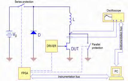
![radiation are no longer [only] an aerospace](/docs-images/96/128545505/images/110-4.jpg "problem.")


110 Particle shower Galactic Cosmic Ray semiconductor failures induced by cosmic radiation are no longer [only] an aerospace problem. Such failure mechanisms must be accounted for in automotive electronics systems design. June 2006 Neutron flux at sea level is 10 5 neutrons/cm 2 -year with E>2 MeV which may cause SEE in electronics
 A neutron")


111 Neutron induced Single Event Effects (SEE) A neutron interacts with a nucleus to produce a heavily ionizing secondary that then causes an anomalous macroscopic effect in a working electronic device

 ENEA Casaccia Roma Tapiro")
112 SEE irradiation experiments IRRADIATION SPECIES Protons Neutrons Heavy ions IRRADIATION FACILITIES INFN LNS Catania Tandem (Heavy ions) Ciclotrone (Protons) INFN LNL Legnaro Tandem (Heavy ions) ENEA Casaccia Roma Tapiro (Neutrons)

113 SEB in a Power Diode
114 Typical test circuit 1MW Ion be am DUT Vbias C i(t) 50W line 50W v(t)
115 Charge Amplification (2D Simulation) kV diode Biasing voltage: 1800V Impacting Ion: 12 C (17MeV) E-field[kV/cm] T=0 25ps 100ps 150ps 230ps 500ps 1ns Electrons-Density [cm ] Depth [ mm] P + N - N + G. Soelkner et al. Charge Carrier Avalanche Multiplication, IEEE TRANSACTIONS ON NUCLEAR SCIENCE, VOL. 47, NO. 6, DECEMBER 2000, pp
116 Diode Currente during a destructive impact Biasing Voltage: 2200V ns Current [A] Time [ns]

![25ps 0 50 100 150 200 250 300 350 400 450 Depth [ mm] 25ps 50ps 75ps 100ps 125ps](/docs-images/96/128545505/images/117-3.jpg "75ps 100ps 125ps 300ps 150ps 150ps 10 13 0 50 100 150 200 250 300 350 400 450 Depth")
117 2D Simulation a SEB 400 4kV diode Biasing voltage: 2200V Impacting Ion: 12 C (17MeV) E-field[kV/cm] -3 E-Density [cm ] ps 25ps Depth [ mm] 25ps 50ps 75ps 100ps 125ps 75ps 100ps 125ps 300ps 150ps 150ps Depth [ mm]
118 A double injection like phenomenon E-field[kV/cm] High: Current density Carriers concentration Electric field E-Density [cm ] Depth [ mm] Impact ionization


119 SEE in Power MOSFET SEGR SEB
120 Test circuit GPIB Oscilloscope Computer for off-line statistical analysis
121 Single Event Burn-out


122 SEE in power mosfets Numerical simulation activity 3D finite element simulations are performed using the ATLAS TCAD simulation tool by Silvaco International. Q r,t N r t t R tc N e e t tc π erfc t LET 3.6 π R 0 2 pairs cm c R t 0 t C 0.124mm 4ps 2ps The simulated elementary cell with its lumped elements and the parameters used to simulate the ionizing track for a bromine ion at 230MeV.

 The")

123 SEE in power mosfets 3D numerical simulation Vds=60V Vds=100V (SEB) The role of the parasitic BJT in the charge generation mechanism.


124 SEE in power mosfets 3D numerical simulation The double injection phenomenon.
![Double injection in Power MOSFET Electric Field [ V/cm ] 2.5 x 10⁵ 2 1.5 1 0.](/docs-images/96/128545505/images/125-2.jpg "5 Electric Field t=700ps x=9mm VDS=60V VDS=100V Hole Concentration [cm -3 ] 2.")

125 Double injection in Power MOSFET Electric Field [ V/cm ] 2.5 x Electric Field t=700ps x=9mm VDS=60V VDS=100V Hole Concentration [cm -3 ] 2.5 x Hole Concentration t=700ps x=9mm Vds=100V Vds=60V Distance [ mm ] Distance [ mm ] Impact ionizzation
126 SEE in gate oxide of Power MOSFET SEGR
127 Single Event Gate Rupture

128 A conceptual model for SEGR Ion track J. R. Brews, et. Al. A Conceptual model for SEGR in Power MOSFET s, IEEE TRANS. ON NUCLEAR SCIENCE, VOL. 40, NO. 6, DECEMBER 1993
129 SEB in IGBTs Emettitore Gate N + P _ P + N _ P + Collettore
130 SEB in IGBTs Emettitore Kathode Gate Gate N + P _ P + R P+ N _ P + Collettore Anode
131 2D simulation of SEB in IGBT W. Kaindl, et. Al. Cosmic Radiation-Induced Failure Mechanism of High Voltage IGBT, Proc. of the 17th ISPSD, May 23-26, 2005, Santa Barbara, CA
132 Thank You for Your attention DIEI Università di Cassino e del Lazio Meridionale Via G. di Biasio, 43, Cassino, Italy busatto@unicas.it
Cosmic Rays induced Single Event Effects in Power Semiconductor Devices
 Cosmic Rays induced Single Event Effects in Power Semiconductor Devices Giovanni Busatto University of Cassino ITALY Outline Introduction Cosmic rays in Space Cosmic rays at Sea Level Radiation Effects
1200 V SiC Super Junction Transistors operating at 250 C with extremely low energy losses for power conversion applications
 1200 V SiC Super Junction Transistors operating at 250 C with extremely low energy losses for power conversion applications Ranbir Singh, Siddarth Sundaresan, Eric Lieser and Michael Digangi GeneSiC Semiconductor,
Switching-Self-Clamping-Mode SSCM, a breakthrough in SOA performance for high voltage IGBTs and Diodes
 Switching-Self-Clamping-Mode, a breakthrough in SOA performance for high voltage IGBTs and M. Rahimo, A. Kopta, S. Eicher, U. Schlapbach, S. Linder ISPSD, May 24, Kitakyushu, Japan Copyright [24] IEEE.
Absolute Maximum Ratings (Per Die)
") PD-9778A IRHLG77 RADIATION HARDENED LOGIC LEVEL POWER MOSFET THRU-HOLE (MO-36AB) V, N-CHANNEL TECHNOLOGY Product Summary Part Number Radiation Level RDS(on) I D IRHLG77 krads(si).285.8a IRHLG73 3 krads(si).285.8a
PD-9778A IRHLG77 RADIATION HARDENED LOGIC LEVEL POWER MOSFET THRU-HOLE (MO-36AB) V, N-CHANNEL TECHNOLOGY Product Summary Part Number Radiation Level RDS(on) I D IRHLG77 krads(si).285.8a IRHLG73 3 krads(si).285.8a
High Voltage SPT + HiPak Modules Rated at 4500V
 High Voltage SPT + HiPak Modules Rated at 45V High Voltage SPT + HiPak Modules Rated at 45V A. Kopta, M. Rahimo, U. Schlapbach, R. Schnell, D. Schneider ABB Switzerland Ltd, Semiconductors, Fabrikstrasse
Absolute Maximum Ratings (Per Die)
") PD-97887 IRHLG7S7 RADIATION HARDENED LOGIC LEVEL POWER MOSFET THRU-HOLE (MO-36AB) V, QUAD N-CHANNEL TECHNOLOGY Product Summary Part Number Radiation Level RDS(on) I D IRHLG7S7 krads(si).33.8a IRHLG7S3
PD-97887 IRHLG7S7 RADIATION HARDENED LOGIC LEVEL POWER MOSFET THRU-HOLE (MO-36AB) V, QUAD N-CHANNEL TECHNOLOGY Product Summary Part Number Radiation Level RDS(on) I D IRHLG7S7 krads(si).33.8a IRHLG7S3
IRHLNM7S7110 2N7609U8
 PD-97888 IRHLNM7S7 RADIATION HARDENED LOGIC LEVEL POWER MOSFET SURFACE MOUNT (SMD-.2) V, N-CHANNEL TECHNOLOGY Product Summary Part Number Radiation Level RDS(on) I D IRHLMN7S7 krads(si).29 6.5A IRHLMN7S3
Fundamentals of Power Semiconductor Devices
 В. Jayant Baliga Fundamentals of Power Semiconductor Devices 4y Spri ringer Contents Preface vii Chapter 1 Introduction 1 1.1 Ideal and Typical Power Switching Waveforms 3 1.2 Ideal and Typical Power Device
Power Devices and Circuits
 COURSE ON Power Devices and Circuits Master degree Electronic Curriculum Teacher: Prof. Dept. of Electronics and Telecommunication Eng. University of Napoli Federico II What is the scope of Power Electronics?
R 7 IRHLNA N7604U2 60V, N-CHANNEL RADIATION HARDENED LOGIC LEVEL POWER MOSFET SURFACE MOUNT (SMD-2) PD-97177C TECHNOLOGY
 PD-97177C TECHNOLOGY") PD-9777C IRHLNA7764 2N764U2 RADIATION HARDENED LOGIC LEVEL POWER MOSFET SURFACE MOUNT (SMD-2) 6V, N-CHANNEL R 7 TECHNOLOGY Product Summary Part Number Radiation Level RDS(on) I D IRHLNA7764 krads(si).2
PD-9777C IRHLNA7764 2N764U2 RADIATION HARDENED LOGIC LEVEL POWER MOSFET SURFACE MOUNT (SMD-2) 6V, N-CHANNEL R 7 TECHNOLOGY Product Summary Part Number Radiation Level RDS(on) I D IRHLNA7764 krads(si).2
2N7622U2 IRHLNA797064
 PD-97174B RADIATION HARDENED LOGIC LEVEL POWER MOSFET SURFACE-MOUNT (SMD-2) 6V, P-CHANNEL TECHNOLOGY Product Summary Part Number Radiation Level RDS(on) I D krads(si).17-56a* IRHLNA79364 3 krads(si).17-56a*
A Study of Switching-Self-Clamping-Mode SSCM as an Over-voltage Protection Feature in High Voltage IGBTs
 A Study of Switching-Self-Clamping-Mode SSCM as an Over-voltage Protection Feature in High Voltage IGBTs M. Rahimo, A. Kopta, S. Eicher, U. Schlapbach, S. Linder ISPSD, May 2005, Santa Barbara, USA Copyright
Part Number Radiation Level RDS(on) I D IRHLUC7970Z4 100 krads(si) A IRHLUC7930Z4 300 krads(si) A LCC-6
 I D IRHLUC7970Z4 100 krads(si) A IRHLUC7930Z4 300 krads(si) A LCC-6") PD-97574A RADIATION HARDENED LOGIC LEVEL POWER MOSFET SURFACE MOUNT (LCC-6) 6V, DUAL P-CHANNEL R 7 TECHNOLOGY Product Summary Part Number Radiation Level RDS(on) I D krads(si).6 -.65A IRHLUC793Z4 3 krads(si).6
PD-97574A RADIATION HARDENED LOGIC LEVEL POWER MOSFET SURFACE MOUNT (LCC-6) 6V, DUAL P-CHANNEL R 7 TECHNOLOGY Product Summary Part Number Radiation Level RDS(on) I D krads(si).6 -.65A IRHLUC793Z4 3 krads(si).6
R 7 2N7624U3 IRHLNJ V, P-CHANNEL RADIATION HARDENED LOGIC LEVEL POWER MOSFET SURFACE MOUNT (SMD-0.5) PD-97302D TECHNOLOGY.
 PD-97302D TECHNOLOGY.") PD-9732D 2N7624U3 IRHLNJ79734 RADIATION HARDENED LOGIC LEVEL POWER MOSFET SURFACE MOUNT (SMD-.5) 6V, P-CHANNEL R 7 TECHNOLOGY Product Summary Part Number Radiation Level RDS(on) I D IRHLNJ79734 krads(si).72-22a*
PD-9732D 2N7624U3 IRHLNJ79734 RADIATION HARDENED LOGIC LEVEL POWER MOSFET SURFACE MOUNT (SMD-.5) 6V, P-CHANNEL R 7 TECHNOLOGY Product Summary Part Number Radiation Level RDS(on) I D IRHLNJ79734 krads(si).72-22a*
POWER MOSFET SURFACE MOUNT (SMD-1) 200V, N-CHANNEL. Absolute Maximum Ratings PD-94236C
 200V, N-CHANNEL. Absolute Maximum Ratings PD-94236C") PD-94236C RADIATION HARDENED POWER MOSFET SURFACE MOUNT (SMD-) IRHN5725SE 2V, N-CHANNEL 5 TECHNOLOGY Product Summary Part Number Radiation Level RDS(on) ID IRHN5725SE K Rads (Si).6Ω 3A SMD- International
PD-94236C RADIATION HARDENED POWER MOSFET SURFACE MOUNT (SMD-) IRHN5725SE 2V, N-CHANNEL 5 TECHNOLOGY Product Summary Part Number Radiation Level RDS(on) ID IRHN5725SE K Rads (Si).6Ω 3A SMD- International
IRHF7230 JANSR2N V, N-CHANNEL REF: MIL-PRF-19500/601 RAD-Hard HEXFET TECHNOLOGY RADIATION HARDENED POWER MOSFET THRU-HOLE (TO-39)
") PD - 90672E RADIATION HARDENED POWER MOSFET THRU-HOLE (TO-39) Product Summary Part Number Radiation Level RDS(on) ID QPL Part Number IRHF7230 100K Rads (Si) 0.35Ω 5.5A JANSR2N7262 IRHF3230 300K Rads (Si)
PD - 90672E RADIATION HARDENED POWER MOSFET THRU-HOLE (TO-39) Product Summary Part Number Radiation Level RDS(on) ID QPL Part Number IRHF7230 100K Rads (Si) 0.35Ω 5.5A JANSR2N7262 IRHF3230 300K Rads (Si)
2N7624U3 LOGIC LEVEL POWER MOSFET SURFACE MOUNT (SMD-0.5) 60V, P-CHANNEL TECHNOLOGY. Absolute Maximum Ratings
 60V, P-CHANNEL TECHNOLOGY. Absolute Maximum Ratings") PD-9732 RADIATION HARDENED LOGIC LEVEL POWER MOSFET SURFACE MOUNT (SMD-.5) 2N7624U3 IRHLNJ79734 6V, P-CHANNEL TECHNOLOGY Product Summary Part Number Radiation Level RDS(on) ID IRHLNJ79734 K Rads (Si).72Ω
PD-9732 RADIATION HARDENED LOGIC LEVEL POWER MOSFET SURFACE MOUNT (SMD-.5) 2N7624U3 IRHLNJ79734 6V, P-CHANNEL TECHNOLOGY Product Summary Part Number Radiation Level RDS(on) ID IRHLNJ79734 K Rads (Si).72Ω
2N7630M2 THRU-HOLE (14-LEAD FLAT PACK) TECHNOLOGY. Product Summary
 TECHNOLOGY. Product Summary") PD-9736 RADIATION HARDENED LOGIC LEVEL POWER MOSFET THRU-HOLE (4-LEAD FLAT PACK) 2N763M2 IRHLA797Z4 6V, Quad P-CHANNEL TECHNOLOGY Product Summary Part Number Radiation Level RDS(on) ID IRHLA797Z4 K Rads
PD-9736 RADIATION HARDENED LOGIC LEVEL POWER MOSFET THRU-HOLE (4-LEAD FLAT PACK) 2N763M2 IRHLA797Z4 6V, Quad P-CHANNEL TECHNOLOGY Product Summary Part Number Radiation Level RDS(on) ID IRHLA797Z4 K Rads
VGS = 4.5V, TC = 25 C Continuous Drain Current 2.6 A
 PD-9726A RADIATION HARDENED LOGIC LEVEL POWER MOSFET SURFACE MOUNT (LCC-28) Product Summary Part Number Radiation Level RDS(on) ID IRHLQ7724 K Rads (Si).Ω 2.6A IRHLQ7324 3K Rads (Si).Ω 2.6A International
IRHNJ63C krads(si) A SMD-0.5
 A SMD-0.5") PD-9798D 2N7598U3 IRHNJ67C3 RADIATION HARDENED POWER MOSFET SURFACE MOUNT (SMD-.5) 6V, N-CHANNEL TECHNOLOGY Product Summary Part Number Radiation Level RDS(on) I D IRHNJ67C3 krads(si) 3. 3.4A IRHNJ63C3
PD-9798D 2N7598U3 IRHNJ67C3 RADIATION HARDENED POWER MOSFET SURFACE MOUNT (SMD-.5) 6V, N-CHANNEL TECHNOLOGY Product Summary Part Number Radiation Level RDS(on) I D IRHNJ67C3 krads(si) 3. 3.4A IRHNJ63C3
Evidence of Gate Voltage Oscillations during Short Circuit of Commercial 1.7 kv/ 1 ka IGBT Power Modules
 Evidence of Gate Voltage Oscillations during Short Circuit of Commercial.7 kv/ ka IGBT Power Modules Paula, Diaz Reigosa, Aalborg University, Denmark, pdr@et.aau.dk Rui, Wu, Aalborg University, Denmark,
2N7606U3 LOGIC LEVEL POWER MOSFET SURFACE MOUNT (SMD-0.5) 60V, N-CHANNEL TECHNOLOGY. Absolute Maximum Ratings
 60V, N-CHANNEL TECHNOLOGY. Absolute Maximum Ratings") PD-973B RADIATION HARDENED LOGIC LEVEL POWER MOSFET SURFACE MOUNT (SMD-.5) Product Summary Part Number Radiation Level RDS(on) ID IRHLNJ7734 K Rads (Si).35Ω 22A* IRHLNJ7334 3K Rads (Si).35Ω 22A* 2N766U3
PD-973B RADIATION HARDENED LOGIC LEVEL POWER MOSFET SURFACE MOUNT (SMD-.5) Product Summary Part Number Radiation Level RDS(on) ID IRHLNJ7734 K Rads (Si).35Ω 22A* IRHLNJ7334 3K Rads (Si).35Ω 22A* 2N766U3
2N7620M2 THRU-HOLE (14-LEAD FLAT PACK) TECHNOLOGY. Product Summary
 TECHNOLOGY. Product Summary") PD-9735 RADIATION HARDENED LOGIC LEVEL POWER MOSFET THRU-HOLE (4-LEAD FLAT PACK) Product Summary Part Number Radiation Level RDS(on) ID IRHLA77Z4 K Rads (Si).6Ω.8A IRHLA73Z4 3K Rads (Si).6Ω.8A 2N762M2
PD-9735 RADIATION HARDENED LOGIC LEVEL POWER MOSFET THRU-HOLE (4-LEAD FLAT PACK) Product Summary Part Number Radiation Level RDS(on) ID IRHLA77Z4 K Rads (Si).6Ω.8A IRHLA73Z4 3K Rads (Si).6Ω.8A 2N762M2
IRHYS9A7130CM JANSR2N7648T3
 PD-97844A RADIATION HARDENED POWER MOSFET THRU-HOLE (Low-Ohmic TO-257AA) V, N-CHANNEL REF: MIL-PRF-95/775 R 9 TECHNOLOGY Product Summary Part Number Radiation Level RDS(on) I D krads (Si) 35m 3A* IRHYS9A33CM
Features. Description. Table 1. Device summary. Quality level. Package. Gold TO-254AA
 Rad-Hard 100 V, 48 A N-channel Power MOSFET Features Datasheet - production data V BDSS I D R DS(on) Q g 100 V 48 A 30 mω 135 nc TO-254AA 3 1 2 Fast switching 100% avalanche tested Hermetic package 50
TECHNOLOGY SURFACE MOUNT (LCC-6) 0.89A -0.65A 0.89A -0.65A
 0.89A -0.65A 0.89A -0.65A") 2N7632UC IRHLUC767Z4 RADIATION HARDENED 6V, Combination N-P-CHANNEL LOGIC LEVEL POWER MOSFET TECHNOLOGY SURFACE MOUNT (LCC-6) Product Summary Part Number Radiation Level R DS(on) I D CHANNEL IRHLUC767Z4
2N7632UC IRHLUC767Z4 RADIATION HARDENED 6V, Combination N-P-CHANNEL LOGIC LEVEL POWER MOSFET TECHNOLOGY SURFACE MOUNT (LCC-6) Product Summary Part Number Radiation Level R DS(on) I D CHANNEL IRHLUC767Z4
IRHY63C30CM 300k Rads(Si) A TO-257AA
 A TO-257AA") PD-95837D 2N7599T3 IRHY67C3CM RADIATION HARDENED POWER MOSFET THRU-HOLE (TO-257AA) 6V, N-CHANNEL TECHNOLOGY Product Summary Part Number Radiation Level RDS(on) I D IRHY67C3CM k Rads(Si) 3. 3.4A IRHY63C3CM
PD-95837D 2N7599T3 IRHY67C3CM RADIATION HARDENED POWER MOSFET THRU-HOLE (TO-257AA) 6V, N-CHANNEL TECHNOLOGY Product Summary Part Number Radiation Level RDS(on) I D IRHY67C3CM k Rads(Si) 3. 3.4A IRHY63C3CM
Discrete 600V GenX3 XPT IGBTs IXAN0072
 Discrete 600V GenX3 XPT IGBTs IXAN0072 Abdus Sattar and Vladimir Tsukanov, Ph.D. IXYS Corporation 1590 Buckeye Drive Milpitas, California 95035 USA 1. Introduction Engineers who design power conversion
IRHNJ57230SE JANSR2N7486U3 R 5 200V, N-CHANNEL REF: MIL-PRF-19500/704 RADIATION HARDENED POWER MOSFET SURFACE MOUNT (SMD-0.5) PD-93836C TECHNOLOGY
 PD-93836C TECHNOLOGY") PD-93836C IRHNJ5723SE RADIATION HARDENED POWER MOSFET SURFACE MOUNT (SMD-.5) 2V, N-CHANNEL REF: MIL-PRF-95/74 R 5 TECHNOLOGY Product Summary Part Number Radiation Level RDS(on) I D QPL Part Number IRHNJ5723SE
PD-93836C IRHNJ5723SE RADIATION HARDENED POWER MOSFET SURFACE MOUNT (SMD-.5) 2V, N-CHANNEL REF: MIL-PRF-95/74 R 5 TECHNOLOGY Product Summary Part Number Radiation Level RDS(on) I D QPL Part Number IRHNJ5723SE
2N7617UC IRHLUC770Z4 60V, DUAL-N CHANNEL RADIATION HARDENED LOGIC LEVEL POWER MOSFET SURFACE MOUNT (LCC-6) Product Summary
 Product Summary") PD-97573 RADIATION HARDENED LOGIC LEVEL POWER MOSFET SURFACE MOUNT (LCC-6) 2N767UC IRHLUC77Z4 6V, DUAL-N CHANNEL TECHNOLOGY Product Summary Part Number Radiation Level RDS(on) ID IRHLUC77Z4 K Rads (Si).75Ω.89A
PD-97573 RADIATION HARDENED LOGIC LEVEL POWER MOSFET SURFACE MOUNT (LCC-6) 2N767UC IRHLUC77Z4 6V, DUAL-N CHANNEL TECHNOLOGY Product Summary Part Number Radiation Level RDS(on) ID IRHLUC77Z4 K Rads (Si).75Ω.89A
IRHNA57264SE JANSR2N7474U2 R 5 250V, N-CHANNEL REF: MIL-PRF-19500/684 RADIATION HARDENED POWER MOSFET SURFACE MOUNT (SMD-2) PD-93816G TECHNOLOGY
 PD-93816G TECHNOLOGY") PD-9386G IRHNA57264SE RADIATION HARDENED POWER MOSFET SURFACE MOUNT (SMD-2) 25V, N-CHANNEL REF: MIL-PRF-95/684 R 5 TECHNOLOGY Product Summary Part Number Radiation Level RDS(on) I D QPL Part Number IRHNA57264SE
PD-9386G IRHNA57264SE RADIATION HARDENED POWER MOSFET SURFACE MOUNT (SMD-2) 25V, N-CHANNEL REF: MIL-PRF-95/684 R 5 TECHNOLOGY Product Summary Part Number Radiation Level RDS(on) I D QPL Part Number IRHNA57264SE
IRHG V, Quad N-CHANNEL RADIATION HARDENED POWER MOSFET THRU-HOLE (MO-036) PD-94432C. 1 TECHNOLOGY. Product Summary MO-036AB
 PD-94432C. 1 TECHNOLOGY. Product Summary MO-036AB") PD-94432C RADIATION HARDENED POWER MOSFET THRU-HOLE (MO-36) Product Summary Part Number Radiation Level RDS(on) ID IRHG57 K Rads (Si).29Ω.6A IRHG53 3K Rads (Si).29Ω.6A IRHG54 5K Rads (Si).29Ω.6A IRHG58
PD-94432C RADIATION HARDENED POWER MOSFET THRU-HOLE (MO-36) Product Summary Part Number Radiation Level RDS(on) ID IRHG57 K Rads (Si).29Ω.6A IRHG53 3K Rads (Si).29Ω.6A IRHG54 5K Rads (Si).29Ω.6A IRHG58
IRHNS57160 R 5 100V, N-CHANNEL. RADIATION HARDENED POWER MOSFET SURFACE MOUNT (SupIR-SMD) PD-97879A TECHNOLOGY. Product Summary
 PD-97879A TECHNOLOGY. Product Summary") PD-97879A IRHNS576 RADIATION HARDENED POWER MOSFET SURFACE MOUNT (SupIR-SMD) V, N-CHANNEL R 5 TECHNOLOGY Product Summary Part Number Radiation Level RDS(on) I D IRHNS576 krads(si).2 75A* IRHNS536 3 krads(si).2
PD-97879A IRHNS576 RADIATION HARDENED POWER MOSFET SURFACE MOUNT (SupIR-SMD) V, N-CHANNEL R 5 TECHNOLOGY Product Summary Part Number Radiation Level RDS(on) I D IRHNS576 krads(si).2 75A* IRHNS536 3 krads(si).2
IRHNJ67234 SURFACE MOUNT (SMD-0.5) PD-97197C REF: MIL-PRF-19500/746. Absolute Maximum Ratings. Product Summary
 PD-97197C REF: MIL-PRF-19500/746. Absolute Maximum Ratings. Product Summary") PD-9797C RADIATION HARDENED POWER MOSFET SURFACE MOUNT (SMD-.5) Product Summary Part Number Radiation Level RDS(on) ID QPL Part Number IRHNJ67234 K Rads (Si).2Ω 2.4A JANSR2N7593U3 IRHNJ63234 3K Rads (Si).2Ω
PD-9797C RADIATION HARDENED POWER MOSFET SURFACE MOUNT (SMD-.5) Product Summary Part Number Radiation Level RDS(on) ID QPL Part Number IRHNJ67234 K Rads (Si).2Ω 2.4A JANSR2N7593U3 IRHNJ63234 3K Rads (Si).2Ω
2 Marks - Question Bank. Unit 1- INTRODUCTION
 Two marks 1. What is power electronics? EE6503 POWER ELECTRONICS 2 Marks - Question Bank Unit 1- INTRODUCTION Power electronics is a subject that concerns the applications electronics principles into situations
IRHY57234CMSE JANSR2N7556T3 R 5 250V, N-CHANNEL REF: MIL-PRF-19500/705 TECHNOLOGY RADIATION HARDENED POWER MOSFET THRU-HOLE(TO-257AA) PD-93823D
 PD-93823D") PD-93823D RADIATION HARDENED POWER MOSFET THRU-HOLE(TO-257AA) 250V, N-CHANNEL REF: MIL-PRF-19500/705 TECHNOLOGY R 5 Product Summary Part Number Radiation Level RDS(on) I D QPL Part Number 100 krads(si)
PD-93823D RADIATION HARDENED POWER MOSFET THRU-HOLE(TO-257AA) 250V, N-CHANNEL REF: MIL-PRF-19500/705 TECHNOLOGY R 5 Product Summary Part Number Radiation Level RDS(on) I D QPL Part Number 100 krads(si)
Published in: Proceedings of the th European Conference on Power Electronics and Applications (EPE'15-ECCE Europe)
") Aalborg Universitet Switching speed limitations of high power IGBT modules Incau, Bogdan Ioan; Trintis, Ionut; Munk-Nielsen, Stig Published in: Proceedings of the 215 17th European Conference on Power
Aalborg Universitet Switching speed limitations of high power IGBT modules Incau, Bogdan Ioan; Trintis, Ionut; Munk-Nielsen, Stig Published in: Proceedings of the 215 17th European Conference on Power
IRHNJ67130 SURFACE MOUNT (SMD-0.5) REF: MIL-PRF-19500/746. Absolute Maximum Ratings PD-95816D. Features: n Low RDS(on) n Fast Switching
 REF: MIL-PRF-19500/746. Absolute Maximum Ratings PD-95816D. Features: n Low RDS(on) n Fast Switching") PD-9586D RADIATION HARDENED POWER MOSFET SURFACE MOUNT (SMD-.5) IRHNJ673 JANSR2N7587U3 V, N-CHANNEL REF: MIL-PRF-95/746 TECHNOLOGY Product Summary Part Number Radiation Level RDS(on) ID QPL Part Number
PD-9586D RADIATION HARDENED POWER MOSFET SURFACE MOUNT (SMD-.5) IRHNJ673 JANSR2N7587U3 V, N-CHANNEL REF: MIL-PRF-95/746 TECHNOLOGY Product Summary Part Number Radiation Level RDS(on) ID QPL Part Number
IRHLMS RADIATION HARDENED LOGIC LEVEL POWER MOSFET THRU-HOLE (Low-Ohmic TO-254AA) 60V, N-CHANNEL TECHNOLOGY PD-97836
 60V, N-CHANNEL TECHNOLOGY PD-97836") PD-97836 IRHLMS7764 RADIATION HARDENED LOGIC LEVEL POWER MOSFET THRU-HOLE (Low-Ohmic TO-254AA) 6V, N-CHANNEL TECHNOLOGY Product Summary Part Number Radiation Level RDS(on) I D IRHLMS7764 krads(si).2 45A*
PD-97836 IRHLMS7764 RADIATION HARDENED LOGIC LEVEL POWER MOSFET THRU-HOLE (Low-Ohmic TO-254AA) 6V, N-CHANNEL TECHNOLOGY Product Summary Part Number Radiation Level RDS(on) I D IRHLMS7764 krads(si).2 45A*
Analog and Telecommunication Electronics
 Politecnico di Torino - ICT School Analog and Telecommunication Electronics F2 Active power devices»mos»bjt» IGBT, TRIAC» Safe Operating Area» Thermal analysis 30/05/2012-1 ATLCE - F2-2011 DDC Lesson F2:
Features. Description. Table 1. Device summary. Gold TO-257AA
 Rad-Hard 100 V, 12 A P-channel Power MOSFET Features Datasheet - production data V DSS I D R DS(on) Q g 100V 12 A 265 mω 40 nc TO-257AA 1 2 3 Fast switching 100% avalanche tested Hermetic package 100 krad
IRHF57034 THRU-HOLE (TO-39) REF: MIL-PRF-19500/701. Absolute Maximum Ratings PD-93791D
 REF: MIL-PRF-19500/701. Absolute Maximum Ratings PD-93791D") PD-9379D RADIATION HARDENED POWER MOSFET THRU-HOLE (TO-39) Product Summary Part Number Radiation Level RDS(on) ID QPL Part Number IRHF5734 K Rads (Si).48Ω 2A* JANSR2N7492T2 IRHF5334 3K Rads (Si).48Ω 2A*
PD-9379D RADIATION HARDENED POWER MOSFET THRU-HOLE (TO-39) Product Summary Part Number Radiation Level RDS(on) ID QPL Part Number IRHF5734 K Rads (Si).48Ω 2A* JANSR2N7492T2 IRHF5334 3K Rads (Si).48Ω 2A*
I D. Operating Junction and -55 to T STG. C Lead Temperature 300 (0.063 in. /1.6 mm from case for 10s) Weight 0.98 (Typical) g
 Weight 0.98 (Typical) g") RADIATION HARDENED POWER MOSFET THRU-HOLE TO-25AF (TO-39) PD-93789G IRHF573 V, N-CHANNEL REF: MIL-PRF-95/7 TECHNOLOGY R 5 Product Summary Part Number Radiation Level RDS(on) QPL Part Number IRHF573 krads(si).8.7a
RADIATION HARDENED POWER MOSFET THRU-HOLE TO-25AF (TO-39) PD-93789G IRHF573 V, N-CHANNEL REF: MIL-PRF-95/7 TECHNOLOGY R 5 Product Summary Part Number Radiation Level RDS(on) QPL Part Number IRHF573 krads(si).8.7a
IRHF57234SE 100 krads(si) A TO-39
 A TO-39") PD-9383C IRHF57234SE RADIATION HARDENED POWER MOSFET THRU-HOLE TO-25AF (TO-39) 25V, N-CHANNEL R 5 TECHNOLOGY Product Summary Part Number Radiation Level RDS(on) I D IRHF57234SE krads(si).42 5.2A TO-39
PD-9383C IRHF57234SE RADIATION HARDENED POWER MOSFET THRU-HOLE TO-25AF (TO-39) 25V, N-CHANNEL R 5 TECHNOLOGY Product Summary Part Number Radiation Level RDS(on) I D IRHF57234SE krads(si).42 5.2A TO-39
AUTOMOTIVE MOSFET. HEXFET Power MOSFET Wiper Control
 AUTOMOTIVE MOSFET PD -94A IRFBA405P Typical Applications Electric Power Steering (EPS) Anti-lock Braking System (ABS) HEXFET Power MOSFET Wiper Control D Climate Control V DSS = 55V Power Door Benefits
SVF4N65T/F(G)/M_Datasheet
/M_Datasheet") 4A, 650V N-CHANNEL MOSFET SVF4N65T/F(G)/M_Datasheet GENERAL DESCRIPTION SVF4N65T/F(G)/M is an N-channel enhancement mode power MOS field effect transistor which is produced using Silan proprietary F-Cell
4A, 650V N-CHANNEL MOSFET SVF4N65T/F(G)/M_Datasheet GENERAL DESCRIPTION SVF4N65T/F(G)/M is an N-channel enhancement mode power MOS field effect transistor which is produced using Silan proprietary F-Cell
IRHNA57Z60 JANSR2N7467U2 R 5 30V, N-CHANNEL REF: MIL-PRF-19500/683 RADIATION HARDENED POWER MOSFET SURFACE MOUNT (SMD-2) PD-91787J TECHNOLOGY
 PD-91787J TECHNOLOGY") PD-91787J IRHNA57Z6 RADIATION HARDENED POWER MOSFET SURFACE MOUNT (SMD-2) Product Summary Part Number Radiation Level RDS(on) I D QPL Part Number IRHNA57Z6 1 krads(si) 3.5m 75A* IRHNA53Z6 3 krads(si) 3.5m
PD-91787J IRHNA57Z6 RADIATION HARDENED POWER MOSFET SURFACE MOUNT (SMD-2) Product Summary Part Number Radiation Level RDS(on) I D QPL Part Number IRHNA57Z6 1 krads(si) 3.5m 75A* IRHNA53Z6 3 krads(si) 3.5m
SVF12N65T/F_Datasheet
 12A, 650V N-CHANNEL MOSFET GENERAL DESCRIPTION SVF12N65T/F is an N-channel enhancement mode power MOS field effect transistor which is produced using Silan proprietary F-Cell TM structure VDMOS technology.
IRHI7360SE. 400V, N-CHANNEL RAD-Hard HEXFET TECHNOLOGY RADIATION HARDENED POWER MOSFET THRU-HOLE (TO-259AA) PD-91446B
 PD-91446B") PD-91446B IRHI7360SE RADIATION HARDENED POWER MOSFET THRU-HOLE (TO-259AA) 400V, N-CHANNEL RAD-Hard HEXFET TECHNOLOGY Product Summary Part Number Radiation Level RDS(on) I D IRHI7360SE 100 krads(si) 0.20
PD-91446B IRHI7360SE RADIATION HARDENED POWER MOSFET THRU-HOLE (TO-259AA) 400V, N-CHANNEL RAD-Hard HEXFET TECHNOLOGY Product Summary Part Number Radiation Level RDS(on) I D IRHI7360SE 100 krads(si) 0.20
A STUDY INTO THE APPLICABILITY OF P + N + (UNIVERSAL CONTACT) TO POWER SEMICONDUCTOR DIODES AND TRANSISTORS FOR FASTER REVERSE RECOVERY
 TO POWER SEMICONDUCTOR DIODES AND TRANSISTORS FOR FASTER REVERSE RECOVERY") Thesis Title: Name: A STUDY INTO THE APPLICABILITY OF P + N + (UNIVERSAL CONTACT) TO POWER SEMICONDUCTOR DIODES AND TRANSISTORS FOR FASTER REVERSE RECOVERY RAGHUBIR SINGH ANAND Roll Number: 9410474 Thesis
Thesis Title: Name: A STUDY INTO THE APPLICABILITY OF P + N + (UNIVERSAL CONTACT) TO POWER SEMICONDUCTOR DIODES AND TRANSISTORS FOR FASTER REVERSE RECOVERY RAGHUBIR SINGH ANAND Roll Number: 9410474 Thesis
IRHN7150 JANSR2N7268U
 PD-90720F IRHN7150 RADIATION HARDENED POWER MOSFET SURFACE MOUNT (SMD-1) 100V, N-CHANNEL REF: MIL-PRF-19500/603 RAD-Hard HEXFET TECHNOLOGY Product Summary Part Number Radiation Level RDS(on) I D IRHN7150
A I T C = 25 C Continuous Drain Current, V 10V (Package Limited) 560 P C = 25 C Power Dissipation 330 Linear Derating Factor
 560 P C = 25 C Power Dissipation 330 Linear Derating Factor") PD - 95758A Features l Designed to support Linear Gate Drive Applications l 175 C Operating Temperature l Low Thermal Resistance Junction - Case l Rugged Process Technology and Design l Fully Avalanche
PD - 95758A Features l Designed to support Linear Gate Drive Applications l 175 C Operating Temperature l Low Thermal Resistance Junction - Case l Rugged Process Technology and Design l Fully Avalanche
IRHNA JANSR2N7524U2 R 5 60V, P-CHANNEL REF: MIL-PRF-19500/733 RADIATION HARDENED POWER MOSFET SURFACE MOUNT (SMD-2) PD-94604D TECHNOLOGY
 PD-94604D TECHNOLOGY") PD-9464D IRHNA59764 RADIATION HARDENED POWER MOSFET SURFACE MOUNT (SMD-2) 6V, P-CHANNEL REF: MIL-PRF-195/733 R 5 TECHNOLOGY Product Summary Part Number Radiation Level RDS(on) I D QPL Part Number IRHNA59764
PD-9464D IRHNA59764 RADIATION HARDENED POWER MOSFET SURFACE MOUNT (SMD-2) 6V, P-CHANNEL REF: MIL-PRF-195/733 R 5 TECHNOLOGY Product Summary Part Number Radiation Level RDS(on) I D QPL Part Number IRHNA59764
14 POWER MODULES
 14 POWER MODULES www.mitsubishichips.com Wide Temperature Operating Range of High Isolation HV-IGBT Modules Mitsubishi Electric has developed new High Voltage Insulated Gate Bipolar Transistor (HV-IGBT)
Impact of Basal Plane Dislocations and Ruggedness of 10 kv 4H-SiC Transistors
 11th International MOS-AK Workshop (co-located with the IEDM and CMC Meetings) Silicon Valley, December 5, 2018 Impact of Basal Plane Dislocations and Ruggedness of 10 kv 4H-SiC Transistors *, A. Kumar,
IRHG V, Combination 2N-2P CHANNEL R TECHNOLOGY RADIATION HARDENED POWER MOSFET THRU-HOLE (MO-036AB) PD-94246D
 PD-94246D") PD-94246D IRHG567 RADIATION HARDENED POWER MOSFET THRU-HOLE (MO-36AB) V, Combination 2N-2P CHANNEL R TECHNOLOGY 5 Product Summary Part Number Radiation Level RDS(on) I D IRHG567 krads(si).29.6a IRHG563
PD-94246D IRHG567 RADIATION HARDENED POWER MOSFET THRU-HOLE (MO-36AB) V, Combination 2N-2P CHANNEL R TECHNOLOGY 5 Product Summary Part Number Radiation Level RDS(on) I D IRHG567 krads(si).29.6a IRHG563
IRHF57133SE THRU-HOLE (TO-39) REF: MIL-PRF-19500/706. Absolute Maximum Ratings
 REF: MIL-PRF-19500/706. Absolute Maximum Ratings") PD - 94334B RADIATION HARDENED POWER MOSFET THRU-HOLE (TO-39) IRHF5733SE JANSR2N7497T2 3V, N-CHANNEL REF: MIL-PRF-95/76 5 TECHNOLOGY Product Summary Part Number Radiation Level RDS(on) ID QPL Part Number
PD - 94334B RADIATION HARDENED POWER MOSFET THRU-HOLE (TO-39) IRHF5733SE JANSR2N7497T2 3V, N-CHANNEL REF: MIL-PRF-95/76 5 TECHNOLOGY Product Summary Part Number Radiation Level RDS(on) ID QPL Part Number
STRH8N10. Rad-Hard 100 V, 6 A N-channel Power MOSFET. Features. Applications. Description
 Rad-Hard 100 V, 6 A N-channel Power MOSFET Features Datasheet - production data V DSS I D R DS(on) Q g 100 V 6 A 0.30 Ω 22 nc SMD.5 Fast switching 100% avalanche tested Hermetic package 50 krad TID SEE
Power Semiconductor Devices
 TRADEMARK OF INNOVATION Power Semiconductor Devices Introduction This technical article is dedicated to the review of the following power electronics devices which act as solid-state switches in the circuits.
IRHNA57064 JANSR2N7468U2 R 5 60V, N-CHANNEL REF: MIL-PRF-19500/673 RADIATION HARDENED POWER MOSFET SURFACE MOUNT (SMD-2) PD-91852J TECHNOLOGY
 PD-91852J TECHNOLOGY") PD-91852J IRHNA5764 RADIATION HARDENED POWER MOSFET SURFACE MOUNT (SMD-2) Product Summary Part Number Radiation Level RDS(on) I D QPL Part Number IRHNA5764 1 krads(si) 5.6m 75A* IRHNA5364 3 krads(si) 5.6m
PD-91852J IRHNA5764 RADIATION HARDENED POWER MOSFET SURFACE MOUNT (SMD-2) Product Summary Part Number Radiation Level RDS(on) I D QPL Part Number IRHNA5764 1 krads(si) 5.6m 75A* IRHNA5364 3 krads(si) 5.6m
IRHNJ597Z30 JANSR2N7519U3 R 5 30V, P-CHANNEL REF: MIL-PRF-19500/732 RADIATION HARDENED POWER MOSFET SURFACE MOUNT (SMD-0.5) PD-94661C TECHNOLOGY
 PD-94661C TECHNOLOGY") PD-9466C IRHNJ597Z3 RADIATION HARDENED POWER MOSFET SURFACE MOUNT (SMD-.5) 3V, P-CHANNEL REF: MIL-PRF-95/732 R 5 TECHNOLOGY Product Summary Part Number Radiation Level RDS(on) I D QPL Part Number IRHNJ597Z3
PD-9466C IRHNJ597Z3 RADIATION HARDENED POWER MOSFET SURFACE MOUNT (SMD-.5) 3V, P-CHANNEL REF: MIL-PRF-95/732 R 5 TECHNOLOGY Product Summary Part Number Radiation Level RDS(on) I D QPL Part Number IRHNJ597Z3
SYNCHRONOUS RECTIFIER SURFACE MOUNT (SMD-2) 60V, N-CHANNEL. Absolute Maximum Ratings PD-94401B
 60V, N-CHANNEL. Absolute Maximum Ratings PD-94401B") PD-9440B RAD-HARD SYNCHRONOUS RECTIFIER SURFACE MOUNT (SMD-2) 60V, N-CHANNEL Product Summary Part Number Radiation Level RDS(on) QG 00K Rads (Si) 6.mΩ 60nC IRHSLNA53064 300K Rads (Si) 6.mΩ 60nC IRHSLNA54064
PD-9440B RAD-HARD SYNCHRONOUS RECTIFIER SURFACE MOUNT (SMD-2) 60V, N-CHANNEL Product Summary Part Number Radiation Level RDS(on) QG 00K Rads (Si) 6.mΩ 60nC IRHSLNA53064 300K Rads (Si) 6.mΩ 60nC IRHSLNA54064
Next Generation Curve Tracing & Measurement Tips for Power Device. Kim Jeong Tae RF/uW Application Engineer Keysight Technologies
 Next Generation Curve Tracing & Measurement Tips for Power Device Kim Jeong Tae RF/uW Application Engineer Keysight Technologies Agenda Page 2 Conventional Analog Curve Tracer & Measurement Challenges
HFI50N06A / HFW50N06A 60V N-Channel MOSFET
 HFI50N06A / HFW50N06A 60V N-Channel MOSFET Features Superior Avalanche Rugged Technology Robust Gate Oxide Technology Very Low Intrinsic Capacitances Excellent Switching Characteristics 100% Avalanche
IRHNM57110 SURFACE MOUNT (SMD-0.2) REF: MIL-PRF-19500/743. Product Summary. Absolute Maximum Ratings PD-97192C
 REF: MIL-PRF-19500/743. Product Summary. Absolute Maximum Ratings PD-97192C") PD-9792C RADIATION HARDENED POWER MOSFET SURFACE MOUNT (SMD-.2) Product Summary IRHNM57 JANSR2N753U8 V, N-CHANNEL REF: MIL-PRF-95/743 5 TECHNOLOGY Part Number Radiation Level RDS(on) ID QPL Part Number
PD-9792C RADIATION HARDENED POWER MOSFET SURFACE MOUNT (SMD-.2) Product Summary IRHNM57 JANSR2N753U8 V, N-CHANNEL REF: MIL-PRF-95/743 5 TECHNOLOGY Part Number Radiation Level RDS(on) ID QPL Part Number
IRHNJ57133SE SURFACE MOUNT (SMD-0.5) REF: MIL-PRF-19500/704 TECHNOLOGY. Absolute Maximum Ratings
 REF: MIL-PRF-19500/704 TECHNOLOGY. Absolute Maximum Ratings") PD - 94294C RADIATION HARDENED POWER MOSFET SURFACE MOUNT (SMD-.5) IRHNJ5733SE JANSR2N7485U3 3V, N-CHANNEL REF: MIL-PRF-95/74 5 TECHNOLOGY Product Summary Part Number Radiation Level RDS(on) ID QPL Part
PD - 94294C RADIATION HARDENED POWER MOSFET SURFACE MOUNT (SMD-.5) IRHNJ5733SE JANSR2N7485U3 3V, N-CHANNEL REF: MIL-PRF-95/74 5 TECHNOLOGY Product Summary Part Number Radiation Level RDS(on) ID QPL Part
SGP100N09T. Symbol Parameter SGP100N09T Unit. 70* -Continuous (TA = 100 )
") SUPER-SEMI SUPER-MOSFET Super Gate Metal Oxide Semiconductor Field Effect Transistor 100V Super Gate Power Transistor SG*100N09T Rev. 1.01 Jun. 2016 SGP100N09T 100V N-Channel MOSFET Description The SG-MOSFET
SUPER-SEMI SUPER-MOSFET Super Gate Metal Oxide Semiconductor Field Effect Transistor 100V Super Gate Power Transistor SG*100N09T Rev. 1.01 Jun. 2016 SGP100N09T 100V N-Channel MOSFET Description The SG-MOSFET
USING F-SERIES IGBT MODULES
 .0 Introduction Mitsubishi s new F-series IGBTs represent a significant advance over previous IGBT generations in terms of total power losses. The device remains fundamentally the same as a conventional
Power Electronics. P. T. Krein
 Power Electronics Day 10 Power Semiconductor Devices P. T. Krein Department of Electrical and Computer Engineering University of Illinois at Urbana-Champaign 2011 Philip T. Krein. All rights reserved.
Absolute Maximum Ratings for Each N-Channel Device
 PD-967D IRHG7 RADIATION HARDENED POWER MOSFET THRU-HOLE (MO-36AB) V, QUAD N CHANNEL RAD-Hard HEXFET TECHNOLOGY Product Summary Part Number Radiation Level RDS(on) I D IRHG7 krads(si).6.a IRHG3 3 krads(si).7.a
IRHNJ V, N-CHANNEL POWER MOSFET SURFACE MOUNT (SMD-0.5) REF: MIL-PRF-19500/703. Absolute Maximum Ratings. Product Summary
 REF: MIL-PRF-19500/703. Absolute Maximum Ratings. Product Summary") PD-93754G RADIATION HARDENED POWER MOSFET SURFACE MOUNT (SMD-.5) Product Summary Part Number Radiation Level RDS(on) ID QPL Part Number IRHNJ573 K Rads (Si).6Ω 22A* JANSR2N748U3 IRHNJ533 3K Rads (Si).6Ω
PD-93754G RADIATION HARDENED POWER MOSFET SURFACE MOUNT (SMD-.5) Product Summary Part Number Radiation Level RDS(on) ID QPL Part Number IRHNJ573 K Rads (Si).6Ω 22A* JANSR2N748U3 IRHNJ533 3K Rads (Si).6Ω
2N7582T1 IRHMS V, N-CHANNEL. RADIATION HARDENED POWER MOSFET THRU-HOLE (Low-Ohmic TO-254AA) Absolute Maximum Ratings PD-96958B
 Absolute Maximum Ratings PD-96958B") PD-96958B RADIATION HARDENED POWER MOSFET THRU-HOLE (Low-Ohmic TO-254AA) 2N7582T IRHMS6764 5V, N-CHANNEL TECHNOLOGY Product Summary Part Number Radiation Level RDS(on) ID IRHMS6764 K Rads (Si).9Ω 45A*
PD-96958B RADIATION HARDENED POWER MOSFET THRU-HOLE (Low-Ohmic TO-254AA) 2N7582T IRHMS6764 5V, N-CHANNEL TECHNOLOGY Product Summary Part Number Radiation Level RDS(on) ID IRHMS6764 K Rads (Si).9Ω 45A*
Power MOSFET Zheng Yang (ERF 3017,
 ECE442 Power Semiconductor Devices and Integrated Circuits Power MOSFET Zheng Yang (ERF 3017, email: yangzhen@uic.edu) Evolution of low-voltage (
UNISONIC TECHNOLOGIES CO., LTD
 UNISONIC TECHNOLOGIES CO., LTD 20A, 150V N-CHANNEL POWER MOSFET DESCRIPTION The UTC 20N15V is a N-Channel POWER MOSFET, it uses UTC s advanced technology to provide customers with high switching speed
UNISONIC TECHNOLOGIES CO., LTD
 UNISONIC TECHNOLOGIES CO., LTD 13A, 500V N-CHANNEL POWER MOSFET DESCRIPTION The UTC 13N50 is an N-Channel enhancement mode power MOSFET. The device adopts planar stripe and uses DMOS technology to minimize
How to Design an R g Resistor for a Vishay Trench PT IGBT
 VISHAY SEMICONDUCTORS www.vishay.com Rectifiers By Carmelo Sanfilippo and Filippo Crudelini INTRODUCTION In low-switching-frequency applications like DC/AC stages for TIG welding equipment, the slow leg
Base part number Package Type Standard Pack Orderable Part Number. IRFP7530PbF TO-247 Tube 25 IRFP7530PbF I D, T J = 25 C 50
 I D, Drain Current (A) StrongIRFET Application Brushed Motor drive applications BLDC Motor drive applications Battery powered circuits Half-bridge and full-bridge topologies Synchronous rectifier applications
IRHLMS RADIATION HARDENED LOGIC LEVEL POWER MOSFET THRU-HOLE (Low-Ohmic TO-254AA) 60V, P-CHANNEL TECHNOLOGY PD-95860
 60V, P-CHANNEL TECHNOLOGY PD-95860") PD-9586 IRHLMS79764 RADIATION HARDENED LOGIC LEVEL POWER MOSFET THRU-HOLE (Low-Ohmic TO-254AA) 6V, P-CHANNEL TECHNOLOGY Product Summary Part Number Radiation Level RDS(on) I D IRHLMS79764 krads(si).8-45a*
PD-9586 IRHLMS79764 RADIATION HARDENED LOGIC LEVEL POWER MOSFET THRU-HOLE (Low-Ohmic TO-254AA) 6V, P-CHANNEL TECHNOLOGY Product Summary Part Number Radiation Level RDS(on) I D IRHLMS79764 krads(si).8-45a*
Introduction. Figure 2: The HiPak standard (left) and high-insulation (right) modules with 3300V SPT + IGBT technology.
 and high-insulation (right) modules with 3300V SPT + IGBT technology.") M. Rahimo, U. Schlapbach, A. Kopta, R. Schnell, S. Linder ABB Switzerland Ltd, Semiconductors, Fabrikstrasse 3, CH 5600 Lenzburg, Switzerland email: munaf.rahimo@ch.abb.com Abstract: Following the successful
M. Rahimo, U. Schlapbach, A. Kopta, R. Schnell, S. Linder ABB Switzerland Ltd, Semiconductors, Fabrikstrasse 3, CH 5600 Lenzburg, Switzerland email: munaf.rahimo@ch.abb.com Abstract: Following the successful
QPL Part Number JANSR2N7270 IRHM krads(si) A JANSF2N7270 IRHM krads(si) A JANSG2N7270 JANSH2N7270 TO-254
 A JANSF2N7270 IRHM krads(si) A JANSG2N7270 JANSH2N7270 TO-254") PD-90673C IRHM7450 RADIATION HARDENED POWER MOSFET THRU-HOLE (TO-254AA) 500V, N-CHANNEL REF: MIL-PRF-19500/603 RAD-Hard HEXFET TECHNOLOGY Product Summary Part Number Radiation Level RDS(on) I D IRHM7450
PD-90673C IRHM7450 RADIATION HARDENED POWER MOSFET THRU-HOLE (TO-254AA) 500V, N-CHANNEL REF: MIL-PRF-19500/603 RAD-Hard HEXFET TECHNOLOGY Product Summary Part Number Radiation Level RDS(on) I D IRHM7450
UNISONIC TECHNOLOGIES CO., LTD
 UNISONIC TECHNOLOGIES CO., LTD 10A, 800V N-CHANNEL POWER MOSFET DESCRIPTION The UTC uses UTC s advanced proprietary, planar stripe, DMOS technology to provide excellent R DS(ON), low gate charge and operation
This chapter describes precautions for actual operation of the IGBT module.
 Chapter 5 Precautions for Use 1. Maximum Junction Temperature T vj(max) 5-2 2. Short-Circuit Protection 5-2 3. Over Voltage Protection and Safety Operation Area 5-2 4. Operation Condition and Dead time
UNISONIC TECHNOLOGIES CO., LTD
 UNISONIC TECHNOLOGIES CO., LTD 12A, 800V N-CHANNEL POWER MOSFET DESCRIPTION The UTC 12N80 is an N-channel enhancement mode power MOSFET using UTC s advanced technology to provide customers with planar
IRHNA9160 JANSR2N7425U
 PD-91433D IRHNA9160 RADIATION HARDENED POWER MOSFET SURFACE MOUNT (SMD-2) 100V, P-CHANNEL REF: MIL-PRF-19500/655 RAD-Hard HEXFET TECHNOLOGY Product Summary Part Number Radiation Level RDS(on) I D QPL Part
18 N Amps, 500 Volts N-CHANNEL MOSFET. Power MOSFET DESCRIPTION FEATURES SYMBOL
 Power MOSFET 8 Amps, 500 Volts NCHANNEL MOSFET DESCRIPTION The YR 8N50 are NChannel enhancement mode power field effect transistors (MOSFET) which are produced using YR s proprietary,planar stripe, DMOS
Orderable Part Number IRFP4768PbF TO-247AC Tube 25 IRFP4768PbF
 Application High Efficiency Synchronous Rectification in SMPS Uninterruptible Power Supply High Speed Power Switching Hard Switched and High Frequency Circuits G D S HEXFET Power MOSFET V DSS R DS(on)
HFP4N65F / HFS4N65F 650V N-Channel MOSFET
 HFP4N65F / HFS4N65F 650V N-Channel MOSFET Features Originative New Design Very Low Intrinsic Capacitances Excellent Switching Characteristics 100% Avalanche Tested RoHS Compliant Key Parameters May 2016
N-channel Enhancement mode TO-262/TO-263/TO-220F MOSFET TO-262 TO Gate 2. Drain 3. Source
 N-channel Enhancement mode TO-262/TO-263/TO-220F MOSFET Features High ruggedness Low R DS(ON) (Typ 0.23Ω)@V GS =10V Low Gate Charge (Typ 42nC) Improved dv/dt Capability 100% Avalanche Tested Application:
Semiconductor Devices
 Semiconductor Devices Modelling and Technology Source Electrons Gate Holes Drain Insulator Nandita DasGupta Amitava DasGupta SEMICONDUCTOR DEVICES Modelling and Technology NANDITA DASGUPTA Professor Department
Failure Mechanisms and Robustness of Wide Band-Gap Devices under short-circuits and unclamped inductive switching
 Failure Mechanisms and Robustness of Wide Band-Gap Devices under short-circuits and unclamped inductive switching Stéphane Lefebvre (Cnam), Zoubir Khatir (IFSTTAR), Mounira Berkani (UPEC), Denis Labrousse
IRHNM SURFACE MOUNT (SMD-0.2) REF: MIL-PRF-19500/749. Product Summary. Absolute Maximum Ratings
 REF: MIL-PRF-19500/749. Product Summary. Absolute Maximum Ratings") PD-9779B RADIATION HARDENED POWER MOSFET SURFACE MOUNT (SMD-.2) Product Summary IRHNM597 JANSR2N756U8 V, P-CHANNEL REF: MIL-PRF-95/749 5 TECHNOLOGY Part Number Radiation Level RDS(on) ID QPL Part Number
PD-9779B RADIATION HARDENED POWER MOSFET SURFACE MOUNT (SMD-.2) Product Summary IRHNM597 JANSR2N756U8 V, P-CHANNEL REF: MIL-PRF-95/749 5 TECHNOLOGY Part Number Radiation Level RDS(on) ID QPL Part Number
MBN3600E17F Silicon N-channel IGBT 1700V F version
 Silicon N-channel IGBT 17V F version Spec.No.IGBT-SP-124 R P1 FEATURES Soft switching behavior & low conduction loss: Soft low-injection punch-through with trench gate IGBT. Low driving power: Low input
Avalanche Ruggedness of 800V Lateral IGBTs in Bulk Si
 Avalanche Ruggedness of 800V Lateral IGBTs in Bulk Si Gianluca Camuso 1, Nishad Udugampola 2, Vasantha Pathirana 2, Tanya Trajkovic 2, Florin Udrea 1,2 1 University of Cambridge, Engineering Department
Insulated Gate Bipolar Transistor (IGBT)
") nsulated Gate Bipolar Transistor (GBT) Comparison between BJT and MOS power devices: BJT MOS pros cons pros cons low V O thermal instability thermal stability high R O at V MAX > 400 V high C current complex
nsulated Gate Bipolar Transistor (GBT) Comparison between BJT and MOS power devices: BJT MOS pros cons pros cons low V O thermal instability thermal stability high R O at V MAX > 400 V high C current complex
AUTOMOTIVE MOSFET. C Soldering Temperature, for 10 seconds 300 (1.6mm from case )
") PD -95487 Typical Applications 42 Volts Automotive Electrical Systems Electrical Power Steering (EPS) Integrated Starter Alternator Lead-Free Benefits Ultra Low On-Resistance Dynamic dv/dt Rating 75 C
PD -95487 Typical Applications 42 Volts Automotive Electrical Systems Electrical Power Steering (EPS) Integrated Starter Alternator Lead-Free Benefits Ultra Low On-Resistance Dynamic dv/dt Rating 75 C
T C =25 unless otherwise specified
 800V N-Channel MOSFET FEATURES Originative New Design Superior Avalanche Rugged Technology Robust Gate Oxide Technology Very Low Intrinsic Capacitances Excellent Switching Characteristics Unrivalled Gate
SVF18N50F/T/PN_Datasheet
 18A 500V N-CHANNEL MOSFET GENERAL DESCRIPTION SVF18N50F/T/PN is an N-channel enhancement mode power MOS field effect transistor which is produced using Silan proprietary F-Cell TM structure VDMOS technology.
UNISONIC TECHNOLOGIES CO., LTD
 UNISONIC TECHNOLOGIES CO., LTD 15A, 500V N-CHANNEL POWER MOSFET DESCRIPTION The UTC is an N-channel mode power MOSFET using UTC s advanced technology to provide customers with planar stripe and DMOS technology.
HCD6N70S / HCU6N70S 700V N-Channel Super Junction MOSFET
 HCD6N70S / HCU6N70S 700V N-Channel Super Junction MOSFET FEATURES Originative New Design Superior Avalanche Rugged Technology Robust Gate Oxide Technology Very Low Intrinsic Capacitances Excellent Switching
GGVF4N60F/FG/T/K/M/MJ 4A, 600V, N-Channel MOSFET
 General Description The GGVF4N60D/F/FG/T/K/M/MJ is an N-channel enhancement mode power MOS field effect transistor. The improved planar stripe cell and the improved guard ring terminal have been especially