Public. Introduction to ASML. Ron Kool. SVP Corporate Strategy and Marketing. March-2015 Veldhoven
|
|
|
- Gwendolyn Summers
- 6 years ago
- Views:
Transcription


1 Public Introduction to ASML Ron Kool SVP Corporate Strategy and Marketing March-2015 Veldhoven
2 More than 200 billion ICs are made every year IC units, in billions In 2014, 219 billion ICs were produced 30 for every man, woman and child on the planet. Global semiconductor industry sales were $305.6 billion. Public Slide 2 January Data: WSTS
3 ASML makes machines for making those chips Public Slide 3 January 2015 Lithography is the critical tool/process step for producing chips


4 From shed to world leader.. Slide 4 March 2015

 and Philips.")


5 Introducing ASML Slide 5 March 2015 Headquarter in Veldhoven Netherlands Original name ASM Lithography Founded in 1984 as JV between the Dutch companies Advanced Semiconductor Materials International (ASMI) and Philips ASMI withdraws, 1994 Philips decides to pull out IPO in 1995 Amsterdam/NASDAQ Market capitalization ~40BEuro Business: Lithography for semi-conductors; main product: wafer stepper Customers: Intel, Samsung, tsmc, SK Hynix.. Over 70 sales and service offices worldwide

 Today: More than a billion")
6 Driving the semiconductor industry: Moore s Law Gordon Moore (1965 April 19 th ): Number of transistors per chip doubles every year. Prediction later was elevated to law Later adjusted to two years, the trend has held for five decades. Slide 6 March 2015 Key to maintaining the law is making smaller transistors Transistor length has shrunk by a million The first integrated circuit on silicon, on a wafer the size of a fingernail (Fairchild Semiconductor, 1959) Today: More than a billion transistors on the same area (Intel, 2012)


7 Our success is based on providing superior products that enable Moore s law Company secret Our focused strategy enabled us to deliver superior products to the market resulting in a steady increase of our market share ASML Litho market share % Stepper Scanner Twinscan Immersion EUV 85% Source: Gartner, S&P Capital IQ, ASML 7

8 Moore s law value creation Market Value: - The market value driven by Moore s Law amounted to $13 Trillion in This is equal to three-quarters of the entire economy of the United States. Confidential Slide 8 10 March 2015 VLSI Research Inc 8


9 We expect Moore s law to continue due to end-user demand growth Company secret Further penetration of current applications through new features and cost down Smartphones, B units Tablets, B units Servers, M units # cores/server will also grow % p.a % p.a % p.a New applications are enabled by higher performance and lower cost Wearables, B units Connected devices, B units N/A % p.a % p.a Source: Euromonitor, Gartner, Yankee group, Profound Market intelligence, Machina Research's M2M forecasts 9
 ASML (2) AMAT (1) TEL (1) (7)")
 (49) (35) EMC Software and services (27) Yahoo (1) (14) (14) (4) (7) (20) Total EBIT 2013 = ~250")
10 ebay (4) Facebook (3) Tencent (3) Hitachi (4) Toshiba (3) Dell (3) in an ecosystem that has considerable financial means and strong incentives to drive innovation Top technology companies in our ecosystem (EBIT 2013, B$) ASML (2) AMAT (1) TEL (1) (7) ASML Peers Semi Other Company secret Semi equipment Semi manufacturers (13) (8) TI (3) Semi design (12) Ericsson (4) (5) Hardware manufacturers (8) (49) (35) EMC Software and services (27) Yahoo (1) (14) (14) (4) (7) (20) Total EBIT 2013 = ~250 B$ 10
 Resolution: 19 nanometers after double patterning Overlay: As")

11 Keeping up with Moore s Law Resolution: 1200 nanometers Overlay: 300 nanometers 40 wafers per hour (100mm wafers) Resolution: 19 nanometers after double patterning Overlay: As little as 1 nanometer Public Slide 11 January wafers per hour (300 mm wafers) PAS 2000 ASML s first stepper, 1984 TWINSCAN NXT:1970Ci The most advanced immersion scanner, 2013

12 The next step: EUV Large vacuum chamber Resolution: <10 nanometers after double patterning Public Slide 12 January 2015 New light source Mirror optics
13 Innovation at ASML Innovation in existing product markets Product/process innovation Eco-system innovation Business model innovation Incubation of new businesses External venturing Public Slide 13 January 2015


14 How to make an Integrated Circuit Slide 14 March 2015 deposition Lithography process diagnostics Track (put resist on) resist expose mask Etch Track (develop) Ion implant


15 Open Innovation from design to manufacturing Customers Public Slide 15 January 2015 Ecosystem Suppliers Academia Technology partners Advanced Research Center for Nanolithography

16 Product/process innovation Ship and iterate. Introduction of immersion technology The industry moved immersion from initial feasibility studies into production in less than four years. Early immersion versions of ASML TWINSCAN systems gave chipmakers the opportunity to test and develop immersion technology in preparation for volume-manufacturing. Slide 16 March 2015 October 2003: Redirection from 157nm to immersion (193nm based) August of 2004 ASML ships a 1 st version to Albany NanoTech at the University of Albany SUNY (State University of New York). At that time more than 16 chipmakers had already used the machine to run 10,000 test wafers. End ASML ships the 2 nd version of its immersion tool, the TWINSCAN XT:1250i, to TSMC, IMEC and Applied Materials, Inc. In 2005, introduction of a 3 rd version - convertible scanner for dry or wet lithography, the TWINSCAN XT:1400. This tool gave customers the flexibility to include immersion in their technology road maps while protecting their investments in dry 193-nm technology. In 2006 ASML shipped the 4 th generation of its immersion exposure tool, the ASML TWINSCAN XT:1700i, included new lens technology (catadioptric), used in High Volume Manufacturing In 2006, ASML announces the XT:1900i, NA of 1.35.

17 Product/process innovation - virtual integration with suppliers Leveraging ASML s and suppliers individual competencies To optimize performance, flexibility, and risk exposure Through seamless, open, and trusted collaboration, Ultimately working as if it were one enterprise Confidential Slide March 2015 Technology leadership Roadmap alignment and performance Serviceability, testability and manufacturability PGP Customer Intimacy Operational Excellence Cost, productivity and uptime Timely delivery


18 Open innovation in our operating model Suppliers Public Slide March 2015 Components, Assy & Module assembly Module assembly Final assembly Customer Order & Delivery Assembly & Test ~ 600 Suppliers, of which 40 partners represent 80% of purchasing value ~ buys (modules & parts) in one platform, where the number of parts in a platform is larger than >85% of system costs from supply base
19 Making optimal use of open innovation: Deciding on what to in- and outsource Public Slide March 2015 Manufacturing competence Unique Litho Non-unique N.A. OEM OEM Whitebox ASML ASML Contract Manufacturer Competencies unique for lithography should be at ASML Competencies non-unique for lithography should be outside ASML Non-unique Unique Litho Development competence


20 Business Models differ per technology and supplier profile Confidential 21 2 September 2013 Stages Supplier Location Business Model : ASML : Netherlands : Make Manufacturing of the WS shortstroke module is done ASML Veldhoven


21 Business Models differ per technology and supplier profile Publicl 22 2 September 2013 Power Electronics Supplier Location Business Model : Prodrive : Netherlands : OEM Prodrive both designs and manufactures power electronics cabinets

22 Business Models differ per technology and supplier profile Public 23 2 September 2013 Handler Supplier Location Business Model : VDL-ETG : Netherlands : TCO responsibility VDL-ETG manufactures wafer handler and has design and sustaining responsibility to secure TCO roadmap

23 Customer Co-invest program EUR 1.38 billion of research and development projects from 2013 through 2017 For the high investments needed, ASML created partnerships with their customers to support the development of new technologies. The Customer Co-Investment Program (CCIP) was initiated in July 2012 To accelerate the development of EUV technology And the development of 450mm technology Slide 24 March 2015 The Participating Customers collectively funded EUR 1.38 billion of research and development projects from 2013 through Risk sharing with largest customers while the results of ASML s development programs available to every semiconductor manufacturer with no restrictions. In addition, the participating customers have invested in ordinary shares equal, in aggregate, to 23 percent of ASML's issued share capital (with restricted voting and trading rights)
24 Connecting (manufacturing) to the design process of the customer Slide 25 March 2015


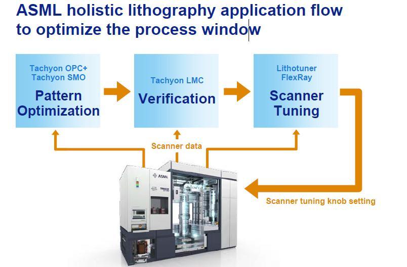
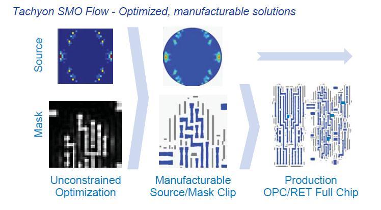
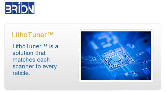
25 Incubation of new business: ASML holistic lithography Confidential Slide January 2014 Scanner 1.Advanced lithography capability (Imaging, overlay and focus) Design context used to identify hotspot and correct them BRION Computational lithography 4- Process window detection Metrology and control SW

26
TWINSCAN XT:1950i Water-based immersion taken to the max Enabling fast, single-exposure lithography at sub 40 nm
 TWINSCAN XT:1950i Water-based immersion taken to the max Enabling fast, single-exposure lithography at sub 40 nm SEMICON West, San Francisco July 14-18, 2008 Slide 1 The immersion pool becomes an ocean
Facing Moore s Law with Model-Driven R&D
 Facing Moore s Law with Model-Driven R&D Markus Matthes Executive Vice President Development and Engineering, ASML Eindhoven, June 11 th, 2015 Slide 2 Contents Introducing ASML Lithography, the driving
DUV. Matthew McLaren Vice President Program Management, DUV. 24 November 2014
 DUV Matthew McLaren Vice President Program Management, DUV 24 Forward looking statements This document contains statements relating to certain projections and business trends that are forward-looking,
Technological Challenges in Semiconductor Lithography
 Technological Challenges in Semiconductor Lithography some aspects of projection lithography technology and its position in high tech industry and academia Ramin Badie ASML Research 2014 What do I want
ASML Market dynamics. Dave Chavoustie EVP Sales Analyst Day, September 30, 2004
 ASML Market dynamics Dave Chavoustie EVP Sales Analyst Day, September 30, 2004 Agenda! Market Overview! Growth Opportunities! 300mm Market! Asia Overview / Slide 2 ASML Unit Market Share Trend 60% 12 &
Competitive in Mainstream Products
 Competitive in Mainstream Products Bert Koek VP, Business Unit manager 300mm Fabs Analyst Day 20 September 2005 ASML Competitive in mainstream products Introduction Market share Device layers critical
Leadership Through Innovation Litho for the future
 Leadership Through Innovation Litho for the future Deutsche Bank Access Asia Conference 2010 Singapore Craig De Young VP Investor Relations and Corporate Communications May 12, 2010 Public Safe Harbor
Bank of America Merrill Lynch Taiwan, Technology and Beyond Conference
 Bank of America Merrill Lynch Taiwan, Technology and Beyond Conference Craig De Young Vice President Investor Relations Taipei, Taiwan March 12, 2013 Forward looking statements Slide 2 Safe Harbor Statement
Holistic View of Lithography for Double Patterning. Skip Miller ASML
 Holistic View of Lithography for Double Patterning Skip Miller ASML Outline Lithography Requirements ASML Holistic Lithography Solutions Conclusions Slide 2 Shrink Continues Lithography keeps adding value
The Development of the Semiconductor CVD and ALD Requirement
 The Development of the Semiconductor CVD and ALD Requirement 1 Linx Consulting 1. We create knowledge and develop unique insights at the intersection of electronic thin film processes and the chemicals
Doug Dunn ASML President and Chief Executive Officer Deutsche Bank Conference London, England September 19, / Slide 1
 Doug Dunn ASML President and Chief Executive Officer Deutsche Bank Conference London, England September 19, 2003 / Slide 1 Safe Harbor Safe Harbor Statement under the U.S. Private Securities Litigation
Enabling Semiconductor Innovation and Growth
 Enabling Semiconductor Innovation and Growth EUV lithography drives Moore s law well into the next decade BAML 2018 APAC TMT Conference Taipei, Taiwan Craig De Young Vice President IR - Asia IR March 14,
Holistic Lithography. Christophe Fouquet. Executive Vice President, Applications. 24 November 2014
 Holistic Lithography Christophe Fouquet Executive Vice President, Applications 24 Holistic Lithography Introduction Customer Problem: Beyond 20nm node scanner and non scanner contributions must be addressed
(Complementary E-Beam Lithography)
") Extending Optical Lithography with C E B L (Complementary E-Beam Lithography) July 13, 2011 4008 Burton Drive, Santa Clara, CA 95054 Outline Complementary Lithography E-Beam Complements Optical Multibeam
Extending Optical Lithography with C E B L (Complementary E-Beam Lithography) July 13, 2011 4008 Burton Drive, Santa Clara, CA 95054 Outline Complementary Lithography E-Beam Complements Optical Multibeam
CLSA Investors Forum 2017
 CLSA Investors Forum 2017 Grand Hyatt Hong Kong Craig De Young Vice President Investor Relations September 11-15 2017 Forward looking statements Slide 2 This document contains statements relating to certain
EUV Supporting Moore s Law
 EUV Supporting Moore s Law Marcel Kemp Director Investor Relations - Europe DB 2014 TMT Conference London September 4, 2014 Forward looking statements This document contains statements relating to certain
EUVL Scanners Operational at Chipmakers. Skip Miller Semicon West 2011
 EUVL Scanners Operational at Chipmakers Skip Miller Semicon West 2011 Outline ASML s Lithography roadmap to support Moore s Law Progress on NXE:3100 (0.25NA) EUV systems Progress on NXE:3300 (0.33NA) EUV
Roadmap Semiconductor Equipment Innovation Agenda
 Roadmap Semiconductor Equipment Innovation Agenda 2018-2021 1. Societal and economic relevance Over the years, electronics have become an inseparable part of our lives. Think of the internet, the cloud,
G450C. Global 450mm Consortium at CNSE. Michael Liehr, General Manager G450C, Vice President for Research
 Global 450mm Consortium at CNSE Michael Liehr, General Manager G450C, Vice President for Research - CNSE Overview - G450C Vision - G450C Mission - Org Structure - Scope - Timeline The Road Ahead for Nano-Fabrication
Multiple Patterning for Immersion Extension and EUV Insertion. Chris Bencher Distinguished Member of Technical Staff Applied Materials CTO group
 Multiple Patterning for Immersion Extension and EUV Insertion Chris Bencher Distinguished Member of Technical Staff Applied Materials CTO group Abstract Multiple Patterning for Immersion Extension and
A Perspective on Semiconductor Equipment. R. B. Herring March 4, 2004
 A Perspective on Semiconductor Equipment R. B. Herring March 4, 2004 Outline Semiconductor Industry Overview of circuit fabrication Semiconductor Equipment Industry Some equipment business strategies Product
EUVL getting ready for volume introduction
 EUVL getting ready for volume introduction SEMICON West 2010 Hans Meiling, July 14, 2010 Slide 1 public Outline ASML s Lithography roadmap to support Moore s Law Progress on 0.25NA EUV systems Progress
Lithography Industry Collaborations
 Accelerating the next technology revolution Lithography Industry Collaborations SOKUDO Breakfast July 13, 2011 Stefan Wurm SEMATECH Copyright 2009 SEMATECH, Inc. SEMATECH, and the SEMATECH logo are registered
Status and challenges of EUV Lithography
 Status and challenges of EUV Lithography SEMICON Europa Dresden, Germany Jan-Willem van der Horst Product Manager EUV October 10 th, 2013 Slide 2 Contents Introduction NXE:3100 NXE:3300B Summary and acknowledgements
The SEMATECH Model: Potential Applications to PV
 Continually cited as the model for a successful industry/government consortium Accelerating the next technology revolution The SEMATECH Model: Potential Applications to PV Dr. Michael R. Polcari President
Economic Impact of the Albany Cluster. Kenneth Adams President & CEO, Commissioner Empire State Development
 Economic Impact of the Albany Cluster Kenneth Adams President & CEO, Commissioner Empire State Development Governor Andrew M. Cuomo Lt. Governor Robert J. Duffy In 2010, industry shipped over $110 billion
PUSHING LITHOGRAPHY TO ENABLE ULTIMATE NANO-ELECTRONICS. LUC VAN DEN HOVE President & CEO imec
 PUSHING LITHOGRAPHY TO ENABLE ULTIMATE NANO-ELECTRONICS LUC VAN DEN HOVE President & CEO imec OUTLINE! Industry drivers! Roadmap extension! Lithography options! Innovation through global collaboration
Intel Technology Journal
 Volume 06 Issue 02 Published, May 16, 2002 ISSN 1535766X Intel Technology Journal Semiconductor Technology and Manufacturing The Intel Lithography Roadmap A compiled version of all papers from this issue
Mask Technology Development in Extreme-Ultraviolet Lithography
 Mask Technology Development in Extreme-Ultraviolet Lithography Anthony Yen September 6, 2013 Projected End of Optical Lithography 2013 TSMC, Ltd 1976 1979 1982 1985 1988 1991 1994 1997 2000 2003 2007 2012
ISMI Industry Productivity Driver
 SEMATECH Symposium Japan September 15, 2010 Accelerating Manufacturing Productivity ISMI Industry Productivity Driver Scott Kramer VP Manufacturing Technology SEMATECH Copyright 2010 SEMATECH, Inc. SEMATECH,
Optics for EUV Lithography
 Optics for EUV Lithography Dr. Sascha Migura, Carl Zeiss SMT GmbH, Oberkochen, Germany 2018 EUVL Workshop June 13 th, 2018 Berkeley, CA, USA The resolution of the optical system determines the minimum
Newer process technology (since 1999) includes :
 includes :") Newer process technology (since 1999) includes : copper metalization hi-k dielectrics for gate insulators si on insulator strained silicon lo-k dielectrics for interconnects Immersion lithography for masks
Newer process technology (since 1999) includes : copper metalization hi-k dielectrics for gate insulators si on insulator strained silicon lo-k dielectrics for interconnects Immersion lithography for masks
From ArF Immersion to EUV Lithography
 From ArF Immersion to EUV Lithography Luc Van den hove Vice President IMEC Outline Introduction 193nm immersion lithography EUV lithography Global collaboration Conclusions Lithography is enabling 1000
Imaging for the next decade
 Imaging for the next decade Martin van den Brink Executive Vice President Products & Technology IMEC Technology Forum 2009 3 June, 2009 Slide 1 Congratulations! ASML and years of making chips better Slide
GIGAPHOTON INTRODUCTION
 GIGAPHOTON INTRODUCTION 15 th September 2017 Tatsuo Enami Director and Senior Executive Officer GIGAPHOTON Copyright Gigaphoton Inc. Outline of Gigaphoton Business Light source business
immersion optics Immersion Lithography with ASML HydroLith TWINSCAN System Modifications for Immersion Lithography by Bob Streefkerk
 immersion optics Immersion Lithography with ASML HydroLith by Bob Streefkerk For more than 25 years, many in the semiconductor industry have predicted the end of optical lithography. Recent developments,
ECSE 6300 IC Fabrication Laboratory Lecture 3 Photolithography. Lecture Outline
 ECSE 6300 IC Fabrication Laboratory Lecture 3 Photolithography Prof. James J. Q. Lu Bldg. CII, Rooms 6229 Rensselaer Polytechnic Institute Troy, NY 12180 Tel. (518)276 2909 e mails: luj@rpi.edu http://www.ecse.rpi.edu/courses/s18/ecse
Discovering Electrical & Computer Engineering. Carmen S. Menoni Professor Week 3 armain.
 Discovering Electrical & Computer Engineering Carmen S. Menoni Professor Week 3 http://www.engr.colostate.edu/ece103/semin armain.html TOP TECH 2012 SPECIAL REPORT IEEE SPECTRUM PAGE 28, JANUARY 2012 P.E.
2010 IRI Annual Meeting R&D in Transition
 2010 IRI Annual Meeting R&D in Transition U.S. Semiconductor R&D in Transition Dr. Peter J. Zdebel Senior VP and CTO ON Semiconductor May 4, 2010 Some Semiconductor Industry Facts Founded in the U.S. approximately
MAPPER: High throughput Maskless Lithography
 MAPPER: High throughput Maskless Lithography Marco Wieland CEA- Leti Alterative Lithography workshop 1 Today s agenda Introduction Applications Qualification of on-tool metrology by in-resist metrology
MEDIA RELEASE FOR IMMEDIATE RELEASE 26 JULY 2016
 MEDIA RELEASE FOR IMMEDIATE RELEASE 26 JULY 2016 A*STAR S IME KICKS OFF CONSORTIA TO DEVELOP ADVANCED PACKAGING SOLUTIONS FOR NEXT-GENERATION INTERNET OF THINGS APPLICATIONS AND HIGH-PERFORMANCE WIRELESS
IMEC update. A.M. Goethals. IMEC, Leuven, Belgium
 IMEC update A.M. Goethals IMEC, Leuven, Belgium Outline IMEC litho program overview ASML ADT status 1 st imaging Tool description Resist projects Screening using interference litho K LUP / Novel resist
Property right statement: Copyright of charts, tables and sentences in this report belongs to
 The Vertical Portal for China Business Intelligence. Semiconductor Equipment Industry Report, 2009 Nov/2009 Property right statement: Copyright of charts, tables and sentences in this report belongs to
450mm silicon wafers specification challenges. Mike Goldstein Intel Corp.
 450mm silicon wafers specification challenges Mike Goldstein Intel Corp. Outline Background 450mm transition program 450mm silicon evolution Mechanical grade wafers (spec case study) Developmental (test)
EUV lithography: today and tomorrow
 EUV lithography: today and tomorrow Vadim Banine, Stuart Young, Roel Moors Dublin, October 2012 Resolution/half pitch, "Shrink" [nm] EUV DPT ArFi ArF KrF Industry roadmap towards < 10 nm resolution Lithography
Optical Microlithography XXVIII
 PROCEEDINGS OF SPIE Optical Microlithography XXVIII Kafai Lai Andreas Erdmann Editors 24-26 February 2015 San Jose, California, United States Sponsored by SPIE Cosponsored by Cymer, an ASML company (United
Lithography in our Connected World
 Lithography in our Connected World SEMI Austin Spring Forum TOP PAN P R INTING CO., LTD MATER IAL SOLUTIONS DIVISION Toppan Printing Co., LTD A Broad-Based Global Printing Company Foundation: January 17,
ASML, Brion and Computational Lithography. Neal Callan 15 October 2008, Veldhoven
 ASML, Brion and Computational Lithography Neal Callan 15 October 2008, Veldhoven Chip makers want shrink to continue (based on the average of multiple customers input) 200 Logic DRAM today NAND Flash Resolution,
Growing the Semiconductor Industry in New York: Challenges and Opportunities
 Accelerating the next technology revolution The SEMATECH New York Experience Growing the Semiconductor Industry in New York: Challenges and Opportunities Dan Armbrust President and CEO, SEMATECH April
2008 European EUVL. EUV activities the EUVL shop future plans. Rob Hartman
 2008 European EUVL EUV activities the EUVL shop future plans Rob Hartman 2007 international EUVL Symposium 28-31 October 2007 2008 international EUVL Symposium 28 Sapporo, September Japan 1 October 2008
Progress due to: Feature size reduction - 0.7X/3 years (Moore s Law). Increasing chip size - 16% per year. Creativity in implementing functions.
. Increasing chip size - 16% per year. Creativity in implementing functions.") Introduction - Chapter 1 Evolution of IC Fabrication 1960 and 1990 integrated t circuits. it Progress due to: Feature size reduction - 0.7X/3 years (Moore s Law). Increasing chip size - 16% per year. Creativity
Introduction - Chapter 1 Evolution of IC Fabrication 1960 and 1990 integrated t circuits. it Progress due to: Feature size reduction - 0.7X/3 years (Moore s Law). Increasing chip size - 16% per year. Creativity
450mm and Moore s Law Advanced Packaging Challenges and the Impact of 3D
 450mm and Moore s Law Advanced Packaging Challenges and the Impact of 3D Doug Anberg VP, Technical Marketing Ultratech SOKUDO Lithography Breakfast Forum July 10, 2013 Agenda Next Generation Technology
Global Artificial Intelligence (AI) Semiconductor Market: Size, Trends & Forecasts ( ) August 2018
 Semiconductor Market: Size, Trends & Forecasts ( ) August 2018") Global Artificial Intelligence (AI) Semiconductor Market: Size, Trends & Forecasts (2018-2022) August 2018 Global Artificial Intelligence (AI) Semiconductor Market: Coverage Executive Summary and Scope
Global Artificial Intelligence (AI) Semiconductor Market: Size, Trends & Forecasts (2018-2022) August 2018 Global Artificial Intelligence (AI) Semiconductor Market: Coverage Executive Summary and Scope
Nanometer Technologies: Where Design and Manufacturing Converge. Walden C. Rhines CHAIRMAN & CEO
 Nanometer Technologies: Where Design and Manufacturing Converge Walden C. Rhines CHAIRMAN & CEO Nanometer Technologies: Where Design and Manufacturing Converge Nanometer technologies make designers aware
EECS 151/251A Spring 2019 Digital Design and Integrated Circuits. Instructors: Wawrzynek. Lecture 8 EE141
 EECS 151/251A Spring 2019 Digital Design and Integrated Circuits Instructors: Wawrzynek Lecture 8 EE141 From the Bottom Up IC processing CMOS Circuits (next lecture) EE141 2 Overview of Physical Implementations
Demonstrating Commitment in the New Veldhoven Demo Lab
 2006 Fall Edition ASML s customer magazine Demonstrating Commitment in the New Veldhoven Demo Lab TWINSCAN XT:1900Gi Immersion into production 8 12 18 3 Editor s note images Colofon 4 ASML in the news
Update on 193nm immersion exposure tool
 Update on 193nm immersion exposure tool S. Owa, H. Nagasaka, Y. Ishii Nikon Corporation O. Hirakawa and T. Yamamoto Tokyo Electron Kyushu Ltd. January 28, 2004 Litho Forum 1 What is immersion lithography?
IBM Research - Zurich Research Laboratory
 October 28, 2010 IBM Research - Zurich Research Laboratory Walter Riess Science & Technology Department IBM Research - Zurich wri@zurich.ibm.com Outline IBM Research IBM Research Zurich Science & Technology
Metrology in the context of holistic Lithography
 Metrology in the context of holistic Lithography Jeroen Ottens Product System Engineer YieldStar, ASML Lithography is at the heart of chip manufacturing Slide 2 25.April.2017 Repeat 30 to 40 times to build
Advanced Packaging Solutions
 Advanced Packaging Solutions by USHIO INC. USHIO s UX Series Providing Advanced Packaging Solutions Page 2 USHIO s UX Series Models Featured @ SEMICON West 2013 Page 2 Large-Size Interposer Stepper UX7-3Di
Nanomanufacturing and Fabrication
 Nanomanufacturing and Fabrication Matthew Margolis http://www.cnm.es/im b/pages/services/im ages/nanofabrication%20laboratory_archivos/im age007.jpg What we will cover! Definitions! Top Down Vs Bottom
Nikon Medium Term Management Plan
 NIKON CORPORATION Mar.30,2006 Nikon Medium Term Management Plan March 30, 2006 NIKON CORPORATION This presentation contains forward-looking statements with respect to future results, performance and achievements
Progress in full field EUV lithography program at IMEC
 Progress in full field EUV lithography program at IMEC A.M. Goethals*, G.F. Lorusso*, R. Jonckheere*, B. Baudemprez*, J. Hermans*, F. Iwamoto 1, B.S. Kim 2, I.S. Kim 2, A. Myers 3, A. Niroomand 4, N. Stepanenko
Intel's 65 nm Logic Technology Demonstrated on 0.57 µm 2 SRAM Cells
 Intel's 65 nm Logic Technology Demonstrated on 0.57 µm 2 SRAM Cells Mark Bohr Intel Senior Fellow Director of Process Architecture & Integration Intel 1 What are We Announcing? Intel has fabricated fully-functional
Lithography Roadmap. without immersion lithography. Node Half pitch. 248nm. 193nm. 157nm EUVL. 3-year cycle: 2-year cycle: imec 2005
 Lithography Roadmap without immersion lithography Node Half pitch 180 nm 130 nm 90 nm 65 nm 45 nm 32 nm 22 nm 250 nm 180 nm 130 nm 90 nm 65 nm 45 nm 32 nm 248nm 193nm 157nm EUVL 3-year cycle: 2-year cycle:
Market and technology trends in advanced packaging
 Close Market and technology trends in advanced packaging Executive OVERVIEW Recent advances in device miniaturization trends have placed stringent requirements for all aspects of product manufacturing.
Double Patterning Combined with Shrink Technique to Extend ArF Lithography for Contact Holes to 22nm Node and Beyond
 Double Patterning Combined with Shrink Technique to Extend ArF Lithography for Contact Holes to 22nm Node and Beyond Xiangqun Miao* a, Lior Huli b, Hao Chen a, Xumou Xu a, Hyungje Woo a, Chris Bencher
Scaling of Semiconductor Integrated Circuits and EUV Lithography
 Scaling of Semiconductor Integrated Circuits and EUV Lithography ( 半導体集積回路の微細化と EUV リソグラフィー ) December 13, 2016 EIDEC (Emerging nano process Infrastructure Development Center, Inc.) Hidemi Ishiuchi 1 OUTLINE
Spring of EUVL: SPIE 2012 AL EUVL Conference Review
 Spring of EUVL: SPIE 2012 AL EUVL Conference Review Vivek Bakshi, EUV Litho, Inc., Austin, Texas Monday, February 20, 2012 The SPIE Advanced Lithography EUVL Conference is usually held close to spring,
Beyond Immersion Patterning Enablers for the Next Decade
 Beyond Immersion Patterning Enablers for the Next Decade Colin Brodsky Manager and Senior Technical Staff Member Patterning Process Development IBM Semiconductor Research & Development Center Hopewell
State-of-the-art device fabrication techniques
 State-of-the-art device fabrication techniques! Standard Photo-lithography and e-beam lithography! Advanced lithography techniques used in semiconductor industry Deposition: Thermal evaporation, e-gun
R&D Status and Key Technical and Implementation Challenges for EUV HVM
 R&D Status and Key Technical and Implementation Challenges for EUV HVM Sam Intel Corporation Agenda Requirements by Process Node EUV Technology Status and Gaps Photoresists Tools Reticles Summary 2 Moore
SUNY Poly in a New Era
 SUNY Poly in a New Era Bahgat Sammakia Interim President, SUNY Polytechnic Institute SUNY Poly in a New Era Overview SUNY Poly is recognized as a global leader in advanced electronics Research and Development,
It s Time for 300mm Prime
 It s Time for 300mm Prime Iddo Hadar Managing Director, 300mm Prime Program Office SEMI Strategic Business Conference Napa Valley, California Tuesday, April 24, 2007 Safe Harbor Statement This presentation
MICROCHIP MANUFACTURING by S. Wolf
 MICROCHIP MANUFACTURING by S. Wolf Chapter 19 LITHOGRAPHY II: IMAGE-FORMATION and OPTICAL HARDWARE 2004 by LATTICE PRESS CHAPTER 19 - CONTENTS Preliminaries: Wave- Motion & The Behavior of Light Resolution
Recent Trends in Semiconductor IC Device Manufacturing
 Recent Trends in Semiconductor IC Device Manufacturing August 2007 Dr. Stephen Daniels Executive Director National Centre for Plasma Moore s Law Moore s First Law Chip Density will double ever 18months.
Nokia Technologies in 2016 Technology to move us forward.
 Business overview Nokia Technologies in 2016 Technology to move us forward. Our advanced technology development and licensing business group, Nokia Technologies, was established with two main objectives:
Triple i - The key to your success
 Triple i - The key to your success The needs and challenges of today s world are becoming ever more demanding. Standards are constantly rising. Creativity, reliability and high performance are basic prerequisites
420 Intro to VLSI Design
 Dept of Electrical and Computer Engineering 420 Intro to VLSI Design Lecture 0: Course Introduction and Overview Valencia M. Joyner Spring 2005 Getting Started Syllabus About the Instructor Labs, Problem
Commercializing Innovation:
 2011 International Symposium on Lithography Extensions: Oct 2011 Commercializing Innovation: Lessons from the lithography cycles Risto Puhakka This report has been reproduced for 2011 International Symposium
The European Semiconductor industry: 2005 Competitiveness Report. DG Enterprise
 The European Semiconductor industry: 2005 Competitiveness Report DG Enterprise EU presentation, Brussels, September 1, 2005 1 EU presentation, Brussels, September 1, 2005 2 EU presentation, Brussels, September
Manufacturing Case Studies: Copy Exactly (CE!) and the two-year cycle at Intel
 and the two-year cycle at Intel") Manufacturing Case Studies: Copy Exactly (CE!) and the two-year cycle at Intel Paolo A. Gargini Director Technology Strategy Intel Fellow 1 Agenda 2-year cycle Copy Exactly Conclusions 2 I see no reason
Manufacturing Case Studies: Copy Exactly (CE!) and the two-year cycle at Intel Paolo A. Gargini Director Technology Strategy Intel Fellow 1 Agenda 2-year cycle Copy Exactly Conclusions 2 I see no reason
Double Patterning Combined with Shrink Technique to Extend ArF Lithography for Contact Holes to 22nm Node and Beyond
 Double Patterning Combined with Shrink Technique to Extend ArF Lithography for Contact Holes to 22nm Node and Beyond Juliet Xiangqun Miao, Lior Huli b, Hao Chen, Xumou Xu, Hyungje Woo, Chris Bencher, Jen
High-NA EUV lithography enabling Moore s law in the next decade
 High-NA EUV lithography enabling Moore s law in the next decade Jan van Schoot, Kars Troost, Alberto Pirati, Rob van Ballegoij, Peter Krabbendam, Judon Stoeldraijer, Erik Loopstra, Jos Benschop, Jo Finders,
Nanomanufacturing and Fabrication By Matthew Margolis
 Nanomanufacturing and Fabrication By Matthew Margolis Manufacturing is the transformation of raw materials into finished goods for sale, or intermediate processes involving the production or finishing
ACCELERATING THE FUTURE OF SEMICONDUCTORS
 ACCELERATING THE FUTURE OF SEMICONDUCTORS 14 PRODUCTION FACILITIES 7R&D FACILITIES 10+ COUNTRIES VERSUM MATERIALS BY THE NUMBERS* *Fiscal year ending September 30, 2018. 250+ CUSTOMERS CORE INDUSTRIES
Driving profitable growth in Greater China. Andy Ho Chief Market Leader Greater China
 Driving profitable growth in Greater China Andy Ho Chief Market Leader Greater China Key takeaways China HealthTech market is the 2 nd largest globally and exhibits continued robust growth with significant
THE WAFER FAB CLEANS IN SEMICONDUCTOR INDUSTRY FROM A MATERIALS SUPPLIER PERSPECTIVE
 THE WAFER FAB CLEANS IN SEMICONDUCTOR INDUSTRY FROM A MATERIALS SUPPLIER PERSPECTIVE Tianniu Rick Chen, Ph.D. General Manager SP&C Business (Surface Preparation & Cleans) OUTLINE Market drivers and challenges
National Projects on Semiconductor in NEDO
 National Projects on Semiconductor in NEDO June 17, 2011 Toru Nakayama New Energy and Industrial Technology Development Organization (NEDO), Japan Contents About NEDO NEDO s projects for semiconductor
CMOS Digital Integrated Circuits Lec 2 Fabrication of MOSFETs
 CMOS Digital Integrated Circuits Lec 2 Fabrication of MOSFETs 1 CMOS Digital Integrated Circuits 3 rd Edition Categories of Materials Materials can be categorized into three main groups regarding their
21 st Annual Needham Growth Conference
 21 st Annual Needham Growth Conference Investor Presentation January 15, 2019 Safe Harbor Statement The information contained in and discussed during this presentation may include forward-looking statements
Guidelines to Promote National Integrated Circuit Industry Development : Unofficial Translation
 Guidelines to Promote National Integrated Circuit Industry Development : Unofficial Translation Ministry of Industry and Information Technology National Development and Reform Commission Ministry of Finance
Collaboration: The Semiconductor Industry s Path to Survival and Growth
 Collaboration: The Semiconductor Industry s Path to Survival and Growth Dr. Michael R. Polcari President and CEO SEMATECH 15 March 2005 3/17/2005 J:\ADMCTR\OCE\M_Polcari\ITPC 10-04 1 Outline Environment
Limitations and Challenges to Meet Moore's Law
 Limitations and Challenges to Meet Moore's Law Sept 10, 2015 Sung Kim sung_kim@amat.com State of the art: cleanroom toolsets metrology analysis module development test & reliability Introduction Why do
UV Nanoimprint Stepper Technology: Status and Roadmap. S.V. Sreenivasan Sematech Litho Forum May 14 th, 2008
 UV Nanoimprint Stepper Technology: Status and Roadmap S.V. Sreenivasan Sematech Litho Forum May 14 th, 2008 Overview Introduction Stepper technology status: Patterning and CD Control Through Etch Alignment
VENTURE-BACKED IPO EXIT ACTIVITY MORE THAN DOUBLES IN Q WITH STRONGEST QUARTER FOR BIOTECH OFFERINGS SINCE 2000
 CONTACTS Laura Cruz Tenor Communications for NVCA 1.917.406.7517 laura@tenorcom.com Lauren Herman Thomson Reuters 1.646.223.5985 lauren.herman@thomsonreuters.com VENTURE-BACKED IPO EXIT ACTIVITY MORE THAN
Technology Transfers Opportunities, Process and Risk Mitigation. Radhika Srinivasan, Ph.D. IBM
 Technology Transfers Opportunities, Process and Risk Mitigation Radhika Srinivasan, Ph.D. IBM Abstract Technology Transfer is quintessential to any technology installation or semiconductor fab bring up.
Digital Swarming. Public Sector Practice Cisco Internet Business Solutions Group
 Digital Swarming The Next Model for Distributed Collaboration and Decision Making Author J.D. Stanley Public Sector Practice Cisco Internet Business Solutions Group August 2008 Based on material originally
SEMICONDUCTOR INDUSTRY ASSOCIATION FACTBOOK
 Factbook 2014 SEMICONDUCTOR INDUSTRY ASSOCIATION FACTBOOK INTRODUCTION The data included in the 2014 SIA Factbook helps demonstrate the strength and promise of the U.S. semiconductor industry and why it
EUV lithography: status, future requirements and challenges
 EUV lithography: status, future requirements and challenges EUVL Dublin Vadim Banine with the help of Rudy Peters, David Brandt, Igor Fomenkov, Maarten van Kampen, Andrei Yakunin, Vladimir Ivanov and many