Scaling of Semiconductor Integrated Circuits and EUV Lithography
|
|
|
- Evan Ferguson
- 5 years ago
- Views:
Transcription
1 Scaling of Semiconductor Integrated Circuits and EUV Lithography ( 半導体集積回路の微細化と EUV リソグラフィー ) December 13, 2016 EIDEC (Emerging nano process Infrastructure Development Center, Inc.) Hidemi Ishiuchi 1
2 OUTLINE Scaling Trend: End of Moore s Law? EUV Lithography: Present Status EUV-FEL as light source for EUV Lithography Conclusion 2


3 Moore s Law is Dead. Long Live Moore s Law. Cover and Table of Contents of IEEE Spectrum, vol. 52, issue 4, April
4 Moore s Law (G. E. Moore, 1965) The complexity for minimum component costs has increased at a rate of roughly a factor of two per year Ref: Gordon E. Moore, Electronics vol. 38, no. 8, pp , 1965 Reprint version: Proc. IEEE vol. 86, no. 1, pp ,

5 Moore s Law after 40 years (functions per chip, microprocessors) 5

6 Functions /chip: 2x per 2 years 6
7 1000 End of Moore's Law? Scaling Trend of Logic LSIs 2011 ITRS - Technology Trends ITRS /10/11 ITRS MPU/ASIC Metal 1 (M1) ½ Pitch (nm) [historical trailing at 2-yr cycle; extended to 2013; then 3- yr cycle] 2009/10/11 ITRS MPU Printed Gate Length (GLpr) (nm) [3-yr cycle from 2011/35.3nm] Nanometers (1e-9) /10/11 ITRS MPU Physical Gate Length (nm) [begin 3.8-yr cycle from 2009/29.0nm] 16nm Year of Production 2011 ITRS: Source: ITRS 2011 Edition Long-Term
8 1000 End of Moore s Law? Scaling Trend of Logic LSIs 2011 ITRS - Technology Trends ITRS 2011 & /10/11 ITRS MPU/ASIC Metal 1 (M1) ½ Pitch (nm) [historical trailing at 2-yr cycle; extended to 2013; then 3- yr cycle] 2009/10/11 ITRS MPU Printed Gate Length (GLpr) (nm) [3-yr cycle from 2011/35.3nm] Nanometers (1e-9) /10/11 ITRS MPU Physical Gate Length (nm) [begin 3.8-yr cycle from 2009/29.0nm] 16/14nm 11/10nm 8/7nm 6/5nm 16nm ITRS Year of Production 2011 ITRS: Metal1 Half Pitch Physical Gate Length (High Performance Logic) Source: ITRS 2011 Edition / ITRS 2015 Edition Long-Term
9 9

10 10
11 11

12 12
13 13
14 14
15 15

16 16
")
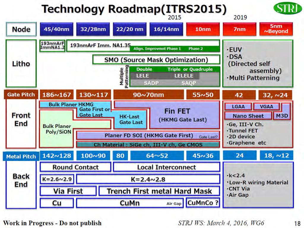
17 More Complex MOSFET Structure (ITRS 2015) 17
18 18
19 19
20 20
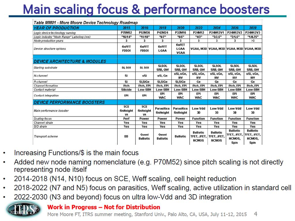
21 Table MM01 - More Moore - Logic Core Device Technology Roadmap YEAR OF PRODUCTION Logic device technology naming P70M56 P48M36 P42M24 P32M20 P24M12G1 P24M12G2 P24M12G3 Logic industry "Node Range" Labeling (nm) "16/14" "11/10" "8/7" "6/5" "4/3" "3/2.5" "2/1.5" Logic device structure options finfet FDSOI Gate TBOX FDSOI finfet FDSOI Gate TBOX FDSOI finfet LGAA finfet LGAA VGAA VGAA, M3D VGAA, M3D VGAA, M3D LOGIC DEVICE GROUND RULES MPU/SoC Metalx ½ Pitch (nm)[1,2] MPU/SoC Metal0/1 ½ Pitch (nm) Contacted poly half pitch (nm) L g: Physical Gate Length for HP Logic (nm) [3] L g: Physical Gate Length for LP Logic (nm) Scaling of MOSFET Table MM01 - More Moore - Logic Core Device Technology Roadmap YEAR OF PRODUCTION Logic device technology naming P70M56 P48M36 P42M24 P32M20 P24M12G1 P24M12G2 P24M12G3 Logic industry "Node Range" Labeling (nm) "16/14" "11/10" "8/7" "6/5" "4/3" "3/2.5" "2/1.5" Logic device structure options finfet finfet finfet finfet VGAA, LGAA FDSOI FDSOI LGAA M3D VGAA VGAA, M3D VGAA, M3D FDSOI FDSOI Gate Gate TBOX TBOX LOGIC DEVICE GROUND RULES MPU/SoC Metalx ½ Pitch (nm)[1,2] MPU/SoC Metal0/1 ½ Pitch (nm) Contacted poly half pitch (nm) L g : Physical Gate Length for HP Logic (nm) [3] L g : Physical Gate Length for LP Logic (nm) finfet: fin Field Effect Transistor LGAA: Lateral Gate-All-Around M3D: Monolithic 3 Dimensional FDSOI: Fully Depleted Silicon On Wafer VGAA: Vertical Gate-All-Around Source: ITRS 2015 Edition, More Moore Chapter, Table MM01 21

22 22
 Floating Gate Cell (intel / Micron)")
23 3D Cell Arrays of NAND Flash Memories Charge Trap Cell (Samsung) Floating Gate Cell (intel / Micron) 23
24 Rayleigh s Formula λ R = k 1 NA R: Resolution (nm) k 1 : Constant λ: Wave Length (nm) NA: Numerical Aperture R (nm) k 1 λ (nm) (ArF) 193 (ArF) 13.5 (EUV) 13.5 (EUV) 13.5 (EUV) NA
 at EIDEC, 2016 International")
25 EUV Lithography Tools in AIST SCR Source: S. Magoshi, et al,, Recent status of the High-NA Small Field Exposure Tool (HSFET) at EIDEC, 2016 International Symposium on Extreme Ultraviolet Lithography, Hiroshima, Japan, Oct. 24,
 at EIDEC, 2016 International")
26 Variable NA NA0.33 vs. NA0.51 Source: S. Magoshi, et al,, Recent status of the High-NA Small Field Exposure Tool (HSFET) at EIDEC, 2016 International Symposium on Extreme Ultraviolet Lithography, Hiroshima, Japan, Oct. 24,
 at EIDEC, 2016 International")
27 HSFET Image Contrast (Simulation) Source: S. Magoshi, et al,, Recent status of the High-NA Small Field Exposure Tool (HSFET) at EIDEC, 2016 International Symposium on Extreme Ultraviolet Lithography, Hiroshima, Japan, Oct. 24,


28 Imaging Performance Quad. Illumination Source: S. Magoshi, et al,, Recent status of the High-NA Small Field Exposure Tool (HSFET) at EIDEC, 2016 International Symposium on Extreme Ultraviolet Lithography, Hiroshima, Japan, Oct. 24,
 at EIDEC, 2016 International Symposium")
29 Imaging Performance Dipole for 11nm L/S Source: S. Magoshi, et al,, Recent status of the High-NA Small Field Exposure Tool (HSFET) at EIDEC, 2016 International Symposium on Extreme Ultraviolet Lithography, Hiroshima, Japan, Oct. 24,


30 Imaging Performance Leaf Dipole for 8nm L/S Source: S. Magoshi, et al,, Recent status of the High-NA Small Field Exposure Tool (HSFET) at EIDEC, 2016 International Symposium on Extreme Ultraviolet Lithography, Hiroshima, Japan, Oct. 24,

31 31
32 32
33 10nm Technology of Samsung Design 10 nm 14 nm Gate pitch 64 nm 78 nm CA pitch 64 nm 78 nm Active Contact Width 18 nm 20 nm M1, Mx (Metal Interconnect) pitch Metal (M1, Mx) half pitch: 24 nm 48 nm 64 nm Lithography Tool: ArF immersion (ArF-i) Ref: H.-J. Cho, et al, 2016 Symposium on VLSI Technology, Digest of Technical Papers, pp.14-15,
34 7 nm Technologies in IEDM 2016 IBM, GLOBALFOUNDRIES, and Samsung: Poly Si (contacted): 44nm / 48 nm pitch (ArF-i) Metal interconnect: 36nm pitch (EUV) EUV lithography for Metal Interconnect TSMC: SRAM cell size: um 2 ArF immersion (ArF-i) lithography (R&D with EUV Lithography, too) Ref: IEDM Technical Digest,

35 IEDM 2016, #2.6, IBM/GF/Samsung Ref: IEDM Technical Digest,


36 IEDM 2016, #2.6, IBM/GF/Samsung Ref: IEDM Technical Digest,
37 2016 EUVL Symposium: Highlights Source 70% average availability achieved. (champion: 90% per 4wks) 1500 wpd demonstrated but consistency is the next challenge. Resist Sensitivity and LER/LCDU are far from targets. Stochastic variation needs to be addressed for current and future materials. Source: Closing Address, 2016 International Symposium on Extreme Ultraviolet Lithography, Hiroshima, Japan, Oct. 26,
38 2016 EUVL Symposium: Highlights Mask Very positive year (ABI optic upgraded, AIMS tool shipped). Blank suppliers making progress (0 defect blanks possible). Infrastructure gap for pattern mask inspection. Pellicle (keeping mask clean) Good progress but very far to go for HVM readiness. Need industry focus to bring all the required components together. Source: Closing Address, 2016 International Symposium on Extreme Ultraviolet Lithography, Hiroshima, Japan, Oct. 26,

39 2016 EUV Focus Areas Source: Closing Address, 2016 International Symposium on Extreme Ultraviolet Lithography, Hiroshima, Japan, Oct. 26,

40 EUV Focus Areas Source: Closing Address, 2016 International Symposium on Extreme Ultraviolet Lithography, Hiroshima, Japan, Oct. 26,

41 EUV-FEL (Free Electron Laser) Source: H. Kawata, Strategy to realize the EUV-FEL high power light source, 2016 International Symposium on Extreme Ultraviolet Lithography, Hiroshima, Japan, Oct. 24,
42 Potential Problems in EUV-FEL R&D expense to develop EUV-FEL Who pays the cost? International collaboration necessary. When and where available? Cost of ownership to be less expensive than existing EUV source Foot print Stable operation two beam lines are necessary for back up Generation of radioactive materials due to high energy electron irradiation High peak power potential damage in mirrors and reticles Resist Too coherent EUV light 42

43 Tradeoff: Resolution vs Sensitivity Low sensitivity is acceptable if higher EUV source power is available. Ref: 2016 International Symposium on Extreme Ultraviolet Lithography, Hiroshima, Japan 43
44 Summary Scaling limit is 10nm for MOSFET gate length; 6nm for metal interconnect, according to ITRS Performance and degree of integration will be getting better by using new device structures, new materials, 3D device structure, 3D assembly & packaging, etc. even if we reach the scaling limit EUV lithography will be used in mass production tool for 7nm or 5nm logic products and beyond. EUV-FEL is a possible solution as an EUV source with higher average power than 1 kw. Its cost of ownership, peak power, coherence of the EUV-FEL source might be the potential problems to be solved 44
45 References ITRS (International Technology Roadmap for Semiconductors) ITRS latest version, and archives White Paper, Presentation Materials, etc. JEITA / STRJ (Semiconductor Technology Roadmap committee of Japan) ITRS 2013 Edition (Japanese version) and older Presentation material of STRJ Workshop, etc. SEMATECH and ISMI Proceedings Archives: Lithography IEUVI (International EUV Initiative)
Present Status and Future Prospects of EUV Lithography
 3rd EUV-FEL Workshop Present Status and Future Prospects of EUV Lithography (EUV リソグラフィーの現状と将来展望 ) December 11, 2011 Evolving nano process Infrastructure Development Center, Inc. (EIDEC) Hidemi Ishiuchi
Advanced Digital Integrated Circuits. Lecture 2: Scaling Trends. Announcements. No office hour next Monday. Extra office hour Tuesday 2-3pm
 EE241 - Spring 20 Advanced Digital Integrated Circuits Lecture 2: Scaling Trends and Features of Modern Technologies Announcements No office hour next Monday Extra office hour Tuesday 2-3pm 2 1 Outline
EUVL getting ready for volume introduction
 EUVL getting ready for volume introduction SEMICON West 2010 Hans Meiling, July 14, 2010 Slide 1 public Outline ASML s Lithography roadmap to support Moore s Law Progress on 0.25NA EUV systems Progress
From ArF Immersion to EUV Lithography
 From ArF Immersion to EUV Lithography Luc Van den hove Vice President IMEC Outline Introduction 193nm immersion lithography EUV lithography Global collaboration Conclusions Lithography is enabling 1000
Intel's 65 nm Logic Technology Demonstrated on 0.57 µm 2 SRAM Cells
 Intel's 65 nm Logic Technology Demonstrated on 0.57 µm 2 SRAM Cells Mark Bohr Intel Senior Fellow Director of Process Architecture & Integration Intel 1 What are We Announcing? Intel has fabricated fully-functional
(Complementary E-Beam Lithography)
") Extending Optical Lithography with C E B L (Complementary E-Beam Lithography) July 13, 2011 4008 Burton Drive, Santa Clara, CA 95054 Outline Complementary Lithography E-Beam Complements Optical Multibeam
Extending Optical Lithography with C E B L (Complementary E-Beam Lithography) July 13, 2011 4008 Burton Drive, Santa Clara, CA 95054 Outline Complementary Lithography E-Beam Complements Optical Multibeam
The future of lithography and its impact on design
 The future of lithography and its impact on design Chris Mack www.lithoguru.com 1 Outline History Lessons Moore s Law Dennard Scaling Cost Trends Is Moore s Law Over? Litho scaling? The Design Gap The
Practical Information
 EE241 - Spring 2010 Advanced Digital Integrated Circuits TuTh 3:30-5pm 293 Cory Practical Information Instructor: Borivoje Nikolić 550B Cory Hall, 3-9297, bora@eecs Office hours: M 10:30am-12pm Reader:
Lithography Roadmap. without immersion lithography. Node Half pitch. 248nm. 193nm. 157nm EUVL. 3-year cycle: 2-year cycle: imec 2005
 Lithography Roadmap without immersion lithography Node Half pitch 180 nm 130 nm 90 nm 65 nm 45 nm 32 nm 22 nm 250 nm 180 nm 130 nm 90 nm 65 nm 45 nm 32 nm 248nm 193nm 157nm EUVL 3-year cycle: 2-year cycle:
Holistic View of Lithography for Double Patterning. Skip Miller ASML
 Holistic View of Lithography for Double Patterning Skip Miller ASML Outline Lithography Requirements ASML Holistic Lithography Solutions Conclusions Slide 2 Shrink Continues Lithography keeps adding value
Multiple Patterning for Immersion Extension and EUV Insertion. Chris Bencher Distinguished Member of Technical Staff Applied Materials CTO group
 Multiple Patterning for Immersion Extension and EUV Insertion Chris Bencher Distinguished Member of Technical Staff Applied Materials CTO group Abstract Multiple Patterning for Immersion Extension and
Mask Technology Development in Extreme-Ultraviolet Lithography
 Mask Technology Development in Extreme-Ultraviolet Lithography Anthony Yen September 6, 2013 Projected End of Optical Lithography 2013 TSMC, Ltd 1976 1979 1982 1985 1988 1991 1994 1997 2000 2003 2007 2012
Newer process technology (since 1999) includes :
 includes :") Newer process technology (since 1999) includes : copper metalization hi-k dielectrics for gate insulators si on insulator strained silicon lo-k dielectrics for interconnects Immersion lithography for masks
Newer process technology (since 1999) includes : copper metalization hi-k dielectrics for gate insulators si on insulator strained silicon lo-k dielectrics for interconnects Immersion lithography for masks
EUVL Scanners Operational at Chipmakers. Skip Miller Semicon West 2011
 EUVL Scanners Operational at Chipmakers Skip Miller Semicon West 2011 Outline ASML s Lithography roadmap to support Moore s Law Progress on NXE:3100 (0.25NA) EUV systems Progress on NXE:3300 (0.33NA) EUV
Update on 193nm immersion exposure tool
 Update on 193nm immersion exposure tool S. Owa, H. Nagasaka, Y. Ishii Nikon Corporation O. Hirakawa and T. Yamamoto Tokyo Electron Kyushu Ltd. January 28, 2004 Litho Forum 1 What is immersion lithography?
National Projects on Semiconductor in NEDO
 National Projects on Semiconductor in NEDO June 17, 2011 Toru Nakayama New Energy and Industrial Technology Development Organization (NEDO), Japan Contents About NEDO NEDO s projects for semiconductor
R&D Status and Key Technical and Implementation Challenges for EUV HVM
 R&D Status and Key Technical and Implementation Challenges for EUV HVM Sam Intel Corporation Agenda Requirements by Process Node EUV Technology Status and Gaps Photoresists Tools Reticles Summary 2 Moore
Intel Technology Journal
 Volume 06 Issue 02 Published, May 16, 2002 ISSN 1535766X Intel Technology Journal Semiconductor Technology and Manufacturing The Intel Lithography Roadmap A compiled version of all papers from this issue
Lithography Industry Collaborations
 Accelerating the next technology revolution Lithography Industry Collaborations SOKUDO Breakfast July 13, 2011 Stefan Wurm SEMATECH Copyright 2009 SEMATECH, Inc. SEMATECH, and the SEMATECH logo are registered
Low-Power VLSI. Seong-Ook Jung VLSI SYSTEM LAB, YONSEI University School of Electrical & Electronic Engineering
 Low-Power VLSI Seong-Ook Jung 2013. 5. 27. sjung@yonsei.ac.kr VLSI SYSTEM LAB, YONSEI University School of Electrical & Electronic Engineering Contents 1. Introduction 2. Power classification & Power performance
NANOELECTRONIC TECHNOLOGY: CHALLENGES IN THE 21st CENTURY
 NANOELECTRONIC TECHNOLOGY: CHALLENGES IN THE 21st CENTURY S. M. SZE National Chiao Tung University Hsinchu, Taiwan And Stanford University Stanford, California ELECTRONIC AND SEMICONDUCTOR INDUSTRIES
Practical Information
 EE241 - Spring 2013 Advanced Digital Integrated Circuits MW 2-3:30pm 540A/B Cory Practical Information Instructor: Borivoje Nikolić 509 Cory Hall, 3-9297, bora@eecs Office hours: M 11-12, W 3:30pm-4:30pm
Optics for EUV Lithography
 Optics for EUV Lithography Dr. Sascha Migura, Carl Zeiss SMT GmbH, Oberkochen, Germany 2018 EUVL Workshop June 13 th, 2018 Berkeley, CA, USA The resolution of the optical system determines the minimum
Advanced Patterning Techniques for 22nm HP and beyond
 Advanced Patterning Techniques for 22nm HP and beyond An Overview IEEE LEOS (Bay Area) Yashesh A. Shroff Intel Corporation Aug 4 th, 2009 Outline The Challenge Advanced (optical) lithography overview Flavors
Nikon EUVL Development Progress Update
 Nikon EUVL Development Progress Update Takaharu Miura EUVL Symposium September 29, 2008 EUVL Symposium 2008 @Lake Tahoe T. Miura September 29, 2008 Slide 1 Presentation Outline 1. Nikon EUV roadmap 2.
450mm and Moore s Law Advanced Packaging Challenges and the Impact of 3D
 450mm and Moore s Law Advanced Packaging Challenges and the Impact of 3D Doug Anberg VP, Technical Marketing Ultratech SOKUDO Lithography Breakfast Forum July 10, 2013 Agenda Next Generation Technology
Computational Lithography Requirements & Challenges for Mask Making. Naoya Hayashi, Dai Nippon Printing Co., Ltd
 Computational Lithography Requirements & Challenges for Mask Making Naoya Hayashi, Dai Nippon Printing Co., Ltd Contents Introduction Lithography Trends Computational lithography options More Complex OPC
Litho Metrology. Program
 Litho Metrology Program John Allgair, Ph.D. Litho Metrology Manager (Motorola assignee) john.allgair@sematech.org Phone: 512-356-7439 January, 2004 National Nanotechnology Initiative Workshop on Instrumentation
TSMC Property. EUV Lithography. The March toward HVM. Anthony Yen. 9 September TSMC, Ltd
 EUV Lithography The March toward HVM Anthony Yen 9 September 2016 1 1 st EUV lithography setup and results, 1986 Si Stencil Mask SR W/C Multilayer Coating Optics λ=11 nm, provided by synchrotron radiation
Progress due to: Feature size reduction - 0.7X/3 years (Moore s Law). Increasing chip size - 16% per year. Creativity in implementing functions.
. Increasing chip size - 16% per year. Creativity in implementing functions.") Introduction - Chapter 1 Evolution of IC Fabrication 1960 and 1990 integrated t circuits. it Progress due to: Feature size reduction - 0.7X/3 years (Moore s Law). Increasing chip size - 16% per year. Creativity
Introduction - Chapter 1 Evolution of IC Fabrication 1960 and 1990 integrated t circuits. it Progress due to: Feature size reduction - 0.7X/3 years (Moore s Law). Increasing chip size - 16% per year. Creativity
PUSHING LITHOGRAPHY TO ENABLE ULTIMATE NANO-ELECTRONICS. LUC VAN DEN HOVE President & CEO imec
 PUSHING LITHOGRAPHY TO ENABLE ULTIMATE NANO-ELECTRONICS LUC VAN DEN HOVE President & CEO imec OUTLINE! Industry drivers! Roadmap extension! Lithography options! Innovation through global collaboration
Acknowledgements. o Stephen Tobin. o Jason Malik. o Dr. Dragan Djurdjanovic. o Samsung Austin Semiconductor, Machine Learning
 Semicon West 2016 Acknowledgements o Stephen Tobin o Samsung Austin Semiconductor, Machine Learning o Jason Malik o Samsung Austin Semiconductor, Metrology o Dr. Dragan Djurdjanovic o University of Texas,
EUV lithography: today and tomorrow
 EUV lithography: today and tomorrow Vadim Banine, Stuart Young, Roel Moors Dublin, October 2012 Resolution/half pitch, "Shrink" [nm] EUV DPT ArFi ArF KrF Industry roadmap towards < 10 nm resolution Lithography
Spring of EUVL: SPIE 2012 AL EUVL Conference Review
 Spring of EUVL: SPIE 2012 AL EUVL Conference Review Vivek Bakshi, EUV Litho, Inc., Austin, Texas Monday, February 20, 2012 The SPIE Advanced Lithography EUVL Conference is usually held close to spring,
Innovation to Advance Moore s Law Requires Core Technology Revolution
 Innovation to Advance Moore s Law Requires Core Technology Revolution Klaus Schuegraf, Ph.D. Chief Technology Officer Silicon Systems Group Applied Materials UC Berkeley Seminar March 9 th, 2012 Innovation
Optical Lithography. Keeho Kim Nano Team / R&D DongbuAnam Semi
 Optical Lithography Keeho Kim Nano Team / R&D DongbuAnam Semi Contents Lithography = Photolithography = Optical Lithography CD : Critical Dimension Resist Pattern after Development Exposure Contents Optical
Trends and Challenges in VLSI Technology Scaling Towards 100nm
 Trends and Challenges in VLSI Technology Scaling Towards 100nm Stefan Rusu Intel Corporation stefan.rusu@intel.com September 2001 Stefan Rusu 9/2001 2001 Intel Corp. Page 1 Agenda VLSI Technology Trends
EUV Supporting Moore s Law
 EUV Supporting Moore s Law Marcel Kemp Director Investor Relations - Europe DB 2014 TMT Conference London September 4, 2014 Forward looking statements This document contains statements relating to certain
Enabling Breakthroughs In Technology
 Enabling Breakthroughs In Technology Mike Mayberry Director of Components Research VP, Technology and Manufacturing Group Intel Corporation June 2011 Defined To be defined Enabling a Steady Technology
Impact of 3-D Mask Effects on CD and Overlay over Image Field in Extreme Ultraviolet Lithography
 Impact of 3-D Mask Effects on CD and Overlay over Image Field in Extreme Ultraviolet Lithography 5 th International EUV Symposium Barcelona, Spain Sven Trogisch Markus Bender Frank-Michael Kamm Disclaimer
Fin-Shaped Field Effect Transistor (FinFET) Min Ku Kim 03/07/2018
 Min Ku Kim 03/07/2018") Fin-Shaped Field Effect Transistor (FinFET) Min Ku Kim 03/07/2018 ECE 658 Sp 2018 Semiconductor Materials and Device Characterizations OUTLINE Background FinFET Future Roadmap Keeping up w/ Moore s Law
Fin-Shaped Field Effect Transistor (FinFET) Min Ku Kim 03/07/2018 ECE 658 Sp 2018 Semiconductor Materials and Device Characterizations OUTLINE Background FinFET Future Roadmap Keeping up w/ Moore s Law
New Process Technologies Will silicon CMOS carry us to the end of the Roadmap?
 HPEC Workshop 2006 New Process Technologies Will silicon CMOS carry us to the end of the Roadmap? Craig L. Keast, Chenson Chen, Mike Fritze, Jakub Kedzierski, Dave Shaver HPEC 2006-1 Outline A brief history
Reliable High Power EUV Source Technology for HVM: LPP or DPP? Vivek Bakshi, Ph.D. EUV Litho, Inc.
 Reliable High Power EUV Source Technology for HVM: LPP or DPP? Vivek Bakshi, Ph.D. EUV Litho, Inc. Presentation Outline Source Technology Requirements Source Technology Performance DPP LPP Technology Trend
Limitations and Challenges to Meet Moore's Law
 Limitations and Challenges to Meet Moore's Law Sept 10, 2015 Sung Kim sung_kim@amat.com State of the art: cleanroom toolsets metrology analysis module development test & reliability Introduction Why do
2008 European EUVL. EUV activities the EUVL shop future plans. Rob Hartman
 2008 European EUVL EUV activities the EUVL shop future plans Rob Hartman 2007 international EUVL Symposium 28-31 October 2007 2008 international EUVL Symposium 28 Sapporo, September Japan 1 October 2008
EE241 - Spring 2013 Advanced Digital Integrated Circuits. Announcements. Sign up for Piazza if you haven t already
 EE241 - Spring 2013 Advanced Digital Integrated Circuits Lecture 2: Scaling Trends and Features of Modern Technologies Announcements Sign up for Piazza if you haven t already 2 1 Assigned Reading R.H.
2009 International Workshop on EUV Lithography
 Contents Introduction Absorber Stack Optimization Non-flatness Correction Blank Defect and Its Mitigation Wafer Printing Inspection Actinic Metrology Cleaning and Repair Status Remaining Issues in EUV
Transistor Scaling in the Innovation Era. Mark Bohr Intel Senior Fellow Logic Technology Development August 15, 2011
 Transistor Scaling in the Innovation Era Mark Bohr Intel Senior Fellow Logic Technology Development August 15, 2011 MOSFET Scaling Device or Circuit Parameter Scaling Factor Device dimension tox, L, W
Eun-Jin Kim, GukJin Kim, Seong-Sue Kim*, Han-Ku Cho*, Jinho Ahn**, Ilsin An, and Hye-Keun Oh
 Eun-Jin Kim, GukJin Kim, Seong-Sue Kim*, Han-Ku Cho*, Jinho Ahn**, Ilsin An, and Hye-Keun Oh Lithography Lab. Department of Applied Physics, Hanyang University, Korea *Samsung Electronics Co., LTD. Korea
Lithography on the Edge
 Lithography on the Edge David Medeiros IBM Prague, Czech Republic 3 October 009 An Edge A line where an something begins or ends: A border, a discontinuity, a threshold Scaling Trend End of an Era? 0000
ECE 5745 Complex Digital ASIC Design Topic 2: CMOS Devices
 ECE 5745 Complex Digital ASIC Design Topic 2: CMOS Devices Christopher Batten School of Electrical and Computer Engineering Cornell University http://www.csl.cornell.edu/courses/ece5950 Simple Transistor
FinFET vs. FD-SOI Key Advantages & Disadvantages
 FinFET vs. FD-SOI Key Advantages & Disadvantages Amiad Conley Technical Marketing Manager Process Diagnostics & Control, Applied Materials ChipEx-2014, Apr 2014 1 Moore s Law The number of transistors
EUVL: Challenges to Manufacturing Insertion
 EUVL: Challenges to Manufacturing Insertion Obert R Wood II International Workshop on EUV Lithography CXRO, LBNL, Berkeley, California 14 June 2017 EUV Critical Issues List EUV Critical Issues, as identified
5. Lithography. 1. photolithography intro: overall, clean room 2. principle 3. tools 4. pattern transfer 5. resolution 6. next-gen
 5. Lithography 1. photolithography intro: overall, clean room 2. principle 3. tools 4. pattern transfer 5. resolution 6. next-gen References: Semiconductor Devices: Physics and Technology. 2 nd Ed. SM
Closed Loop Registration Control (RegC ) Using PROVE as the Data Source for the RegC Process
 Using PROVE as the Data Source for the RegC Process") Invited Paper Closed Loop Registration Control (RegC ) Using PROVE as the Data Source for the RegC Process Erez Graitzer 1 ; Avi Cohen 1 ; Vladimir Dmitriev 1 ; Itamar Balla 1 ; Dan Avizemer 1 Dirk Beyer
Invited Paper Closed Loop Registration Control (RegC ) Using PROVE as the Data Source for the RegC Process Erez Graitzer 1 ; Avi Cohen 1 ; Vladimir Dmitriev 1 ; Itamar Balla 1 ; Dan Avizemer 1 Dirk Beyer
EUV Actinic Blank Inspection Tool Development
 EUV Actinic Blank Inspection Tool Development EUVL Symposium 2011 Hiroki Miyai 1, Tomohiro Suzuki 1, Kiwamu Takehisa 1, Haruhiko Kusunose 1, Takeshi Yamane 2, Tsuneo Terasawa 2, Hidehiro Watanabe 2, Soichi
EECS 151/251A Spring 2019 Digital Design and Integrated Circuits. Instructors: Wawrzynek. Lecture 8 EE141
 EECS 151/251A Spring 2019 Digital Design and Integrated Circuits Instructors: Wawrzynek Lecture 8 EE141 From the Bottom Up IC processing CMOS Circuits (next lecture) EE141 2 Overview of Physical Implementations
Manufacturing Case Studies: Copy Exactly (CE!) and the two-year cycle at Intel
 and the two-year cycle at Intel") Manufacturing Case Studies: Copy Exactly (CE!) and the two-year cycle at Intel Paolo A. Gargini Director Technology Strategy Intel Fellow 1 Agenda 2-year cycle Copy Exactly Conclusions 2 I see no reason
Manufacturing Case Studies: Copy Exactly (CE!) and the two-year cycle at Intel Paolo A. Gargini Director Technology Strategy Intel Fellow 1 Agenda 2-year cycle Copy Exactly Conclusions 2 I see no reason
DUV. Matthew McLaren Vice President Program Management, DUV. 24 November 2014
 DUV Matthew McLaren Vice President Program Management, DUV 24 Forward looking statements This document contains statements relating to certain projections and business trends that are forward-looking,
Lithography. International SEMATECH: A Focus on the Photomask Industry
 Lithography S P E C I A L International SEMATECH: A Focus on the Photomask Industry by Wally Carpenter, International SEMATECH, Inc. (*IBM Corporation Assignee) It is well known that the semiconductor
TECHNOLOGY ROADMAP 2011 EDITION LITHOGRAPHY FOR
 INTERNATIONAL TECHNOLOGY ROADMAP FOR SEMICONDUCTORS 2011 EDITION LITHOGRAPHY THE ITRS IS DEVISED AND INTENDED FOR TECHNOLOGY ASSESSMENT ONLY AND IS WITHOUT REGARD TO ANY COMMERCIAL CONSIDERATIONS PERTAINING
GIGAPHOTON INTRODUCTION
 GIGAPHOTON INTRODUCTION 15 th September 2017 Tatsuo Enami Director and Senior Executive Officer GIGAPHOTON Copyright Gigaphoton Inc. Outline of Gigaphoton Business Light source business
G450C. Global 450mm Consortium at CNSE. Michael Liehr, General Manager G450C, Vice President for Research
 Global 450mm Consortium at CNSE Michael Liehr, General Manager G450C, Vice President for Research - CNSE Overview - G450C Vision - G450C Mission - Org Structure - Scope - Timeline The Road Ahead for Nano-Fabrication
ECSE 6300 IC Fabrication Laboratory Lecture 3 Photolithography. Lecture Outline
 ECSE 6300 IC Fabrication Laboratory Lecture 3 Photolithography Prof. James J. Q. Lu Bldg. CII, Rooms 6229 Rensselaer Polytechnic Institute Troy, NY 12180 Tel. (518)276 2909 e mails: luj@rpi.edu http://www.ecse.rpi.edu/courses/s18/ecse
State-of-the-art device fabrication techniques
 State-of-the-art device fabrication techniques! Standard Photo-lithography and e-beam lithography! Advanced lithography techniques used in semiconductor industry Deposition: Thermal evaporation, e-gun
TWINSCAN XT:1950i Water-based immersion taken to the max Enabling fast, single-exposure lithography at sub 40 nm
 TWINSCAN XT:1950i Water-based immersion taken to the max Enabling fast, single-exposure lithography at sub 40 nm SEMICON West, San Francisco July 14-18, 2008 Slide 1 The immersion pool becomes an ocean
EUV Interference Lithography in NewSUBARU
 EUV Interference Lithography in NewSUBARU Takeo Watanabe 1, Tae Geun Kim 2, Yasuyuki Fukushima 1, Noki Sakagami 1, Teruhiko Kimura 1, Yoshito Kamaji 1, Takafumi Iguchi 1, Yuuya Yamaguchi 1, Masaki Tada
IC Knowledge LLC, PO Box 20, Georgetown, MA Ph: (978) , Fx: (978)
 , Fx: (978)") IC Knowledge LLC, PO Box 20, Georgetown, MA 01833 www.icknowledge.com Ph: (978) 352 7610, Fx: (978) 352 3870 Linx Consulting, PO Box 384, Mendon, MA 01756 0384 www.linxconsulting.com Ph: (617) 273 8837
IC Knowledge LLC, PO Box 20, Georgetown, MA 01833 www.icknowledge.com Ph: (978) 352 7610, Fx: (978) 352 3870 Linx Consulting, PO Box 384, Mendon, MA 01756 0384 www.linxconsulting.com Ph: (617) 273 8837
ITRS MOSFET Scaling Trends, Challenges, and Key Technology Innovations
 Workshop on Frontiers of Extreme Computing Santa Cruz, CA October 24, 2005 ITRS MOSFET Scaling Trends, Challenges, and Key Technology Innovations Peter M. Zeitzoff Outline Introduction MOSFET scaling and
ISSCC 2003 / SESSION 1 / PLENARY / 1.1
 ISSCC 2003 / SESSION 1 / PLENARY / 1.1 1.1 No Exponential is Forever: But Forever Can Be Delayed! Gordon E. Moore Intel Corporation Over the last fifty years, the solid-state-circuits industry has grown
EUV: Status and Challenges Ahead International Workshop on EUVL, Maui 2010
 EUV: Status and Challenges Ahead International Workshop on EUVL, Maui 2010 Jos Benschop Public Agenda Roadmap Status Challenges Summary & conclusion Slide 2 Public Resolution (half pitch) "Shrink" [nm]
Recent Activities of the Actinic Mask Inspection using the EUV microscope at Center for EUVL
 Recent Activities of the Actinic Mask Inspection using the EUV microscope at Center for EUVL Takeo Watanabe, Tetsuo Harada, and Hiroo Kinoshita Center for EUVL, University of Hyogo Outline 1) EUV actinic
Photolithography Technology and Application
 Photolithography Technology and Application Jeff Tsai Director, Graduate Institute of Electro-Optical Engineering Tatung University Art or Science? Lind width = 100 to 5 micron meter!! Resolution = ~ 3
450mm silicon wafers specification challenges. Mike Goldstein Intel Corp.
 450mm silicon wafers specification challenges Mike Goldstein Intel Corp. Outline Background 450mm transition program 450mm silicon evolution Mechanical grade wafers (spec case study) Developmental (test)
EUVL Activities in China
 2014 EUVL Workshop EUVL Activities in China Yanqiu Li, Zhen Cao Beijing Institute of Technology (BIT) Email: liyanqiu@bit.edu.cn Activities only refer to published papers June 25, 2014 OUTLINE Overview
The Development of the Semiconductor CVD and ALD Requirement
 The Development of the Semiconductor CVD and ALD Requirement 1 Linx Consulting 1. We create knowledge and develop unique insights at the intersection of electronic thin film processes and the chemicals
Scope and Limit of Lithography to the End of Moore s Law
 Scope and Limit of Lithography to the End of Moore s Law Burn J. Lin tsmc, Inc. 1 What dictate the end of Moore s Law Economy Device limits Lithography limits 2 Litho Requirement of Critical Layers Logic
Enabling Semiconductor Innovation and Growth
 Enabling Semiconductor Innovation and Growth EUV lithography drives Moore s law well into the next decade BAML 2018 APAC TMT Conference Taipei, Taiwan Craig De Young Vice President IR - Asia IR March 14,
Challenges of EUV masks and preliminary evaluation
 Challenges of EUV masks and preliminary evaluation Naoya Hayashi Electronic Device Laboratory Dai Nippon Printing Co.,Ltd. EUV Mask Workshop 2004 1 Contents Recent Lithography Options on Roadmap Challenges
1 Digital EE141 Integrated Circuits 2nd Introduction
 Digital Integrated Circuits Introduction 1 What is this lecture about? Introduction to digital integrated circuits + low power circuits Issues in digital design The CMOS inverter Combinational logic structures
Growing the Semiconductor Industry in New York: Challenges and Opportunities
 Accelerating the next technology revolution The SEMATECH New York Experience Growing the Semiconductor Industry in New York: Challenges and Opportunities Dan Armbrust President and CEO, SEMATECH April
Introduction. Digital Integrated Circuits A Design Perspective. Jan M. Rabaey Anantha Chandrakasan Borivoje Nikolic. July 30, 2002
 Digital Integrated Circuits A Design Perspective Jan M. Rabaey Anantha Chandrakasan Borivoje Nikolic Introduction July 30, 2002 1 What is this book all about? Introduction to digital integrated circuits.
Photolithography. References: Introduction to Microlithography Thompson, Willson & Bowder, 1994
 Photolithography References: Introduction to Microlithography Thompson, Willson & Bowder, 1994 Microlithography, Science and Technology Sheats & Smith, 1998 Any other Microlithography or Photolithography
Inspection of templates for imprint lithography
 Inspection of templates for imprint lithography Harald F. Hess, a) Don Pettibone, David Adler, and Kirk Bertsche KLA-Tencor 160 Rio Robles, San Jose, California 95134 Kevin J. Nordquist, David P. Mancini,
+1 (479)
") Introduction to VLSI Design http://csce.uark.edu +1 (479) 575-6043 yrpeng@uark.edu Invention of the Transistor Vacuum tubes ruled in first half of 20th century Large, expensive, power-hungry, unreliable
Introduction to VLSI Design http://csce.uark.edu +1 (479) 575-6043 yrpeng@uark.edu Invention of the Transistor Vacuum tubes ruled in first half of 20th century Large, expensive, power-hungry, unreliable
Nano-crystalline Oxide Semiconductor Materials for Semiconductor and Display Technology Sanghun Jeon Ph.D. Associate Professor
 Nano-crystalline Oxide Semiconductor Materials for Semiconductor and Display Technology Sanghun Jeon Ph.D. Associate Professor Department of Applied Physics Korea University Personnel Profile (Affiliation
* AIT-5: Maskless, High-NA, Immersion, EUV, Imprint
 Advanced Issues and Technology (AIT) Modules Purpose: Explain the top advanced issues and concepts in optical projection printing and electron-beam lithography. AIT-1: LER and CAR AIT-2: Resolution Enhancement
Homework 10 posted just for practice. Office hours next week, schedule TBD. HKN review today. Your feedback is important!
 EE141 Fall 2005 Lecture 26 Memory (Cont.) Perspectives Administrative Stuff Homework 10 posted just for practice No need to turn in Office hours next week, schedule TBD. HKN review today. Your feedback
EUV Lithography Transition from Research to Commercialization
 EUV Lithography Transition from Research to Commercialization Charles W. Gwyn and Peter J. Silverman and Intel Corporation Photomask Japan 2003 Pacifico Yokohama, Kanagawa, Japan Gwyn:PMJ:4/17/03:1 EUV
Burn-in & Test Socket Workshop
 Burn-in & Test Socket Workshop IEEE March 3-6, 2002 Hilton Phoenix East/Mesa Hotel Mesa, Arizona IEEE COMPUTER SOCIETY Sponsored By The IEEE Computer Society Test Technology Technical Council COPYRIGHT
EMT 251 Introduction to IC Design
 EMT 251 Introduction to IC Design (Pengantar Rekabentuk Litar Terkamir) Semester II 2011/2012 Introduction to IC design and Transistor Fundamental Some Keywords! Very-large-scale-integration (VLSI) is
Electron Multi-Beam Technology for Mask and Wafer Direct Write. Elmar Platzgummer IMS Nanofabrication AG
 Electron Multi-Beam Technology for Mask and Wafer Direct Write Elmar Platzgummer IMS Nanofabrication AG Contents 2 Motivation for Multi-Beam Mask Writer (MBMW) MBMW Tool Principles and Architecture MBMW
Beyond Immersion Patterning Enablers for the Next Decade
 Beyond Immersion Patterning Enablers for the Next Decade Colin Brodsky Manager and Senior Technical Staff Member Patterning Process Development IBM Semiconductor Research & Development Center Hopewell
write-nanocircuits Direct-write Jaebum Joo and Joseph M. Jacobson Molecular Machines, Media Lab Massachusetts Institute of Technology, Cambridge, MA
 Fab-in in-a-box: Direct-write write-nanocircuits Jaebum Joo and Joseph M. Jacobson Massachusetts Institute of Technology, Cambridge, MA April 17, 2008 Avogadro Scale Computing / 1 Avogadro number s? Intel
Novel EUV Resist Development for Sub-14nm Half Pitch
 EUV Workshop 2015 Maui, HI P64 Novel EUV Resist Development for Sub-14nm Half Pitch Yoshi Hishiro JSR Micro Inc. EUV Workshop, June 17, 2015 1 Contents Requirement for sub-14nm HP EUV resist JSR strategy
Accelerating the next technology revolution
 1 9 8 7 2 0 0 7 EDITION TWELVE - NOVEMBER 2011 report Accelerating the next technology revolution Inside this issue: Realizing the 450mm Transition SEMATECH s October Triple Play Asia Symposium Showcases
Chapter 15 IC Photolithography
 Chapter 15 IC Photolithography Advances in integrated circuit density are driven by the self-fulfilling prophecy known as Moore s law, which specifies that there is an exponential increase in circuit density
HOW TO CONTINUE COST SCALING. Hans Lebon
 HOW TO CONTINUE COST SCALING Hans Lebon OUTLINE Scaling & Scaling Challenges Imec Technology Roadmap Wafer size scaling : 450 mm 2 COST SCALING IMPROVED PERFORMANCE 3 GLOBAL TRAFFIC FORECAST Cloud Traffic
III-V on Si for VLSI. 200 mm III-V on Si. Accelerating the next technology revolution. III-V nfet on 200 mm Si
 III-V on Si for VLSI Accelerating the next technology revolution 200 mm III-V on Si III-V nfet on 200 mm Si R. Hill, C. Park, J. Barnett, J. Huang, N. Goel, J. Oh, W.Y. Loh, J. Price, P. Kirsch, P, Majhi,
AN ANALYSIS: TRADITIONAL SEMICONDUCTOR LITHOGRAPHY VERSUS EMERGING TECHNOLOGY (NANO IMPRINT) Robert L. Wright Kranthi Mitra Adusumilli
 Robert L. Wright Kranthi Mitra Adusumilli") Proceedings of the 2005 Winter Simulation Conference M. E. Kuhl, N. M. Steiger, F. B. Armstrong, and J. A. Joines, eds. AN ANALYSIS: TRADITIONAL SEMICONDUCTOR LITHOGRAPHY VERSUS EMERGING TECHNOLOGY (NANO
Proceedings of the 2005 Winter Simulation Conference M. E. Kuhl, N. M. Steiger, F. B. Armstrong, and J. A. Joines, eds. AN ANALYSIS: TRADITIONAL SEMICONDUCTOR LITHOGRAPHY VERSUS EMERGING TECHNOLOGY (NANO