2009 International Workshop on EUV Lithography
|
|
|
- Doreen Blair
- 5 years ago
- Views:
Transcription


1
2 Contents Introduction Absorber Stack Optimization Non-flatness Correction Blank Defect and Its Mitigation Wafer Printing Inspection Actinic Metrology Cleaning and Repair Status Remaining Issues in EUV Mask & Infra 1
 EUVL 2 nd G EUV PPT 1 st EUV Production 2 nd EUVL Prod. 2009 2010 2011 2012 2013 2014 2")
3 Introduction Samsung s DRAM Roadmap Half Pitch (nm) Minimum Half Pitch Roadmap ArF DPT EUVL 1 st G ( NA = 0.32 ) EUVL 2 nd G EUV PPT 1 st EUV Production 2 nd EUVL Prod
4 Introduction Key Focus Areas in EUVL (2008 EUVL Symposium) Key Focus Areas Ranking Long-term source operation with 100W at IF and 5MJ/day 1 Defect free masks through lifecycle & inspection/review infrastructure 2 Resist resolution, sensitivity & LER met simultaneously 3 Reticle protection during storage, handling and use 4 Projection/illuminator optics and mask lifetime 5 3

5 Issues in EUV Mask Shadowing Effect Non-flatness 6 Imaging Performance Optical Density Carbon Contamination Etch & Cleaning Damage Pit Multilayer Defects Substrate Defects Bump Multilayer Defect Substrate Defect Hardness Defect 4


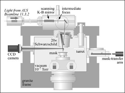
6 EUV Mask Infra IBD Sputter(SEC) EUV Reflectometer(SEC) Ultra Flat(SEC) CSM(Hyogo Univ.) EUV MET(LBNL/SMT) AIT(LBNL/SMT) M7360(SMT) EUV ADT(IMEC/SMT) Ref. Naulleau etal.spie 2005 Ref. Goldberg etal.spie

 H-V Bias Out-of-Phase Condition 0.")
 Best")
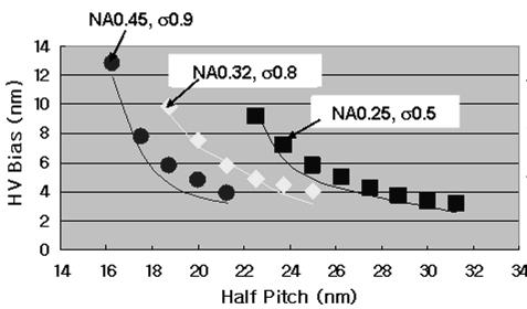
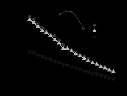
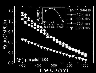
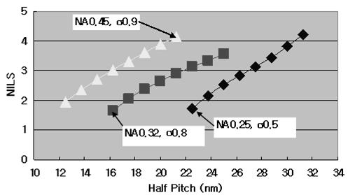
7 Absorber Stack Optimization TaN-Absorber/Si-capping Layer/ML/Qz Substrate Exposed by LBNL MET ( σ = 0.55/0.35 ) H-V Bias Out-of-Phase Condition 0.8 LWR DOF 1st/Oth ratio TaN Thickness (nm) Best Imaging Performance at Out-of-phase thickness 6
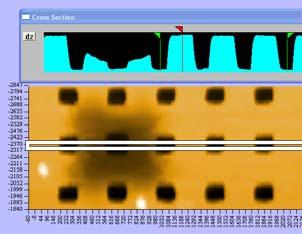
8 Non-flatness Correction Chucking effect of EUV mask with non-flat profile Flatness history Substrate Stress effect ML, Absorber Substrate x F,y F,z F x B,y B,z B Chucking effect ES chuck Substrate Effective flatness: Thickness variation (Frontside flatness) (Backside flatness) x F,y F,z F x B,y B,z B Overlay effect Concave profile of backside Overlay of inward direction U#822 Regi. Overlay (w.r.t U#822) U#884 EUV mask 최진 7
 Non-compensated")


9 Non-flatness Correction IPE OPE (due to Non-flatness) Non-compensated Step0 Flatness check Step1 Chucking regi Step2 Chucking overlay calculation Overlay 3σ ~ 20 nm Step3 Nonflatness regi IPE IPD (due to chucking) Compensated Step4 Sum of Regis Step5 E-beam format Step6 E-beam Grid Correction Overlay 3σ~ 3nm To determine relaxed spec., additional experiments are required. 8
 LTEM (> 80nm) Substrate Defect ML Defect 250 Qz (> 70nm) Defects (ea.")
 = (Defect Density")
10 Blank Defect and Its Mitigation Defect Density in Currently Available Blanks LTEM (> 70nm) LTEM (> 80nm) Substrate Defect ML Defect 250 Qz (> 70nm) Defects (ea.) Qz (> 80nm) / / / / /07 Phase Defect Pareto ~ ~ * ~100X improvement needed * (Defect = (Defect * (Size/25)^
11 Substrate Pit Defect in EUV Mask ArF Mask 2π/λ*(n-1)*h=π (out-of phase) h=λ=193 nm EUV Mask 2π/λ*2*h=π (out-of phase) h=λ/4=3.38 nm h n ~ 1.5 h Transmission Air to Quartz (n=1 vs. n=1.5) Reflection (x2) Vacuum to Vacuum (n=1 vs. n=1) Out-of phase depth in EUV ~ 1/57 of ArF 10


 Smoothing effect due to ML deposition")

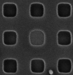
12 Pit Defect Smoothing by ML Deposition Programmed Pit Defect Mask 160nm 50nm 110nm 100nm 170nm 40nm 120nm 90nm 180nm 30nm 130nm 80nm 190nm 20nm 140nm 70nm 200nm 10nm 150nm 60nm No pits (?) Smoothing effect due to ML deposition Before ML depo Width = 67.3 nm, Depth = 24.8 nm After ML depo Width = 59.8 nm, Depth = 8.5 nm 11

 - Best")

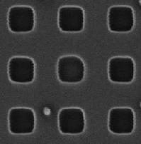
13 Pit Defect Smoothing by ML Deposition Depo. Angle Effect Depo. angle = 55 (SAMSUNG) - Best uniformity & Lower deposition rate Depo. angle = 26 (SEMATECH) - Lowest Defect Density 12


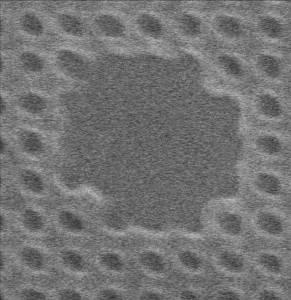
14 Pit Defect Smoothing by ML Deposition AIT Image of PDM after ML Deposition Depo. Angle = 55 Depo. Angle = 26 Not printed Printed 60nm-pit was patterned but not observed by AIT. Possibility of pit smoothing by multilayer deposition 13


")


15 Pattern Placement Defect Mitigation Pattern Placement Fiducial Marking Transform Algorithm Defect-free Fiducial Marking Process Blank Inspection Defect map generation (GDSII) Rotation Defect map matching on mask layout Extraction mask layout around each defect Scanning within marginal area for defect displacement Shift Find effective zero defect yes Standardization of Fiducial Mark, SEMATECH Alignment Accuracy < writer > No Next Blank End 14


16 Pattern Placement Defect Mitigation Fiducial Mark Depth 488 nm wavelength 100 nm depth Fiducial mark signal is maximum at λ/4 depth but E- beam alignment signal has to be considered. Contrast =0.7 (NA0.7/s0.83) 15
 Beam size at mask= 0.8 mm diameter (< 0.5 mm CCD size) CCD 1 frame scan area = 0.5 x 0.5 mm 2 Defect location measurement needs additional review tool!")
17 Pattern Placement Defect Mitigation Requirement for Inspection Infra Actinic Inspection Tool by MIRAI-Selete (SPIE2009) Energy flow rate through ML CCD pixel: 1000 x 1000 (13 um cell size) SC mag. = 26X (13 um cell size 500 nm cell on the mask) Beam size at mask= 0.8 mm diameter (< 0.5 mm CCD size) CCD 1 frame scan area = 0.5 x 0.5 mm 2 Defect location measurement needs additional review tool!! 16


")

18 Wafer Printing Inspection vs Mask Pattern Inspection Design Wafer Printing Inspection 160nm 140nm 120nm 100nm 80nm 60nm 50nm Mask SEM Mask Inspection Wafer(ADT) Inspection Mask Inspection ~ 15nm(1X) Wafer Printing Inspection ~ 33nm(1X) 17


 Mask")

19 Wafer Printing Image of Defect Extrusion Bridge Big Bridge Wafer SEM (ADT) Mask SEM All real defects captured by WPI are repairable!! 18


 Aerial Image Analysis")
20 Coherent Scattering Microscope Aerial Image Emulation by Diffracted Beam Distribution EUV Mask Diffracted Beam Aerial Image EUV Coherent Scattering Microscopy High NA (>0.59 for 4X) Aerial Image Analysis without Aberrations 19
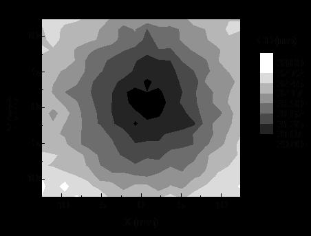
21 Coherent Scattering Microscope PSM Condition HV Bias NILS CD Uniformity Pattern Damage Inspection 20
 ΔR(%)")

22 Cleaning Status Cleaning Chemical Damage Δt of Si & Ru-capping Layer ΔR vs Cleaning Cycle Δt (nm) ΔR(%) Position Ru-capping layer shows much better chemical endurance than Si except O 3 water. ΔR ~ 0.04% after 24 cleaning cycle. 21

23 Repair Status Process Development of E-beam Repair Before Now SEM Image AFM Image Collapsed Undercut Wafer Image Repaired Pattern 22
24 Remaining Issues in EUV Mask & Infrastructure 100x improvement of blank defect density 5x improvement of actinic inspection tool throughput and its commercialization Inexpensive defect review tool for defect location measurement with ~10nm-stage accuracy EUV aerial image defect review tool (EUV-AIMS) Pattern inspection tool for 22nm-HP Proved reticle protection and handling technique 23


25 Thank You 24
EUVL getting ready for volume introduction
 EUVL getting ready for volume introduction SEMICON West 2010 Hans Meiling, July 14, 2010 Slide 1 public Outline ASML s Lithography roadmap to support Moore s Law Progress on 0.25NA EUV systems Progress
Comparison of actinic and non-actinic inspection of programmed defect masks
 Comparison of actinic and non-actinic inspection of programmed defect masks Funded by Kenneth Goldberg, Anton Barty Hakseung Han*, Stefan Wurm*, Patrick Kearney, Phil Seidel Obert Wood*, Bruno LaFontaine
Mask Technology Development in Extreme-Ultraviolet Lithography
 Mask Technology Development in Extreme-Ultraviolet Lithography Anthony Yen September 6, 2013 Projected End of Optical Lithography 2013 TSMC, Ltd 1976 1979 1982 1985 1988 1991 1994 1997 2000 2003 2007 2012
SEMATECH Defect Printability Studies
 Accelerating the next technology revolution SEMATECH Defect Printability Studies Il Yong Jang 1, Jenah Harris-Jones 1, Ranganath Teki 1, Vibhu Jindal 1, Frank Goodwin 1 Masaki Satake 2, Ying Li 2, Danping
Challenges of EUV masks and preliminary evaluation
 Challenges of EUV masks and preliminary evaluation Naoya Hayashi Electronic Device Laboratory Dai Nippon Printing Co.,Ltd. EUV Mask Workshop 2004 1 Contents Recent Lithography Options on Roadmap Challenges
Progresses in NIL Template Fabrication Naoya Hayashi
 Progresses in NIL Template Fabrication Naoya Hayashi Electronic Device Operations Dai Nippon Printing Co., Ltd. Contents 1. Introduction Motivation NIL mask fabrication process 2. NIL mask resolution improvement
UV Nanoimprint Stepper Technology: Status and Roadmap. S.V. Sreenivasan Sematech Litho Forum May 14 th, 2008
 UV Nanoimprint Stepper Technology: Status and Roadmap S.V. Sreenivasan Sematech Litho Forum May 14 th, 2008 Overview Introduction Stepper technology status: Patterning and CD Control Through Etch Alignment
Progress in full field EUV lithography program at IMEC
 Progress in full field EUV lithography program at IMEC A.M. Goethals*, G.F. Lorusso*, R. Jonckheere*, B. Baudemprez*, J. Hermans*, F. Iwamoto 1, B.S. Kim 2, I.S. Kim 2, A. Myers 3, A. Niroomand 4, N. Stepanenko
EUV: Status and Challenges Ahead International Workshop on EUVL, Maui 2010
 EUV: Status and Challenges Ahead International Workshop on EUVL, Maui 2010 Jos Benschop Public Agenda Roadmap Status Challenges Summary & conclusion Slide 2 Public Resolution (half pitch) "Shrink" [nm]
R&D Status and Key Technical and Implementation Challenges for EUV HVM
 R&D Status and Key Technical and Implementation Challenges for EUV HVM Sam Intel Corporation Agenda Requirements by Process Node EUV Technology Status and Gaps Photoresists Tools Reticles Summary 2 Moore
450mm patterning out of darkness Backend Process Exposure Tool SOKUDO Lithography Breakfast Forum July 10, 2013 Doug Shelton Canon USA Inc.
 450mm patterning out of darkness Backend Process Exposure Tool SOKUDO Lithography Breakfast Forum 2013 July 10, 2013 Doug Shelton Canon USA Inc. Introduction Half Pitch [nm] 2013 2014 2015 2016 2017 2018
Development of ultra-fine structure t metrology system using coherent EUV source
 2009 International Workshop On EUV Lithography, July 13-17,2009 Development of ultra-fine structure t metrology system using coherent EUV source University of Hyogo 1, Hiroo Kinoshita 1,3, Tetuo Harada
Process Optimization
 Process Optimization Process Flow for non-critical layer optimization START Find the swing curve for the desired resist thickness. Determine the resist thickness (spin speed) from the swing curve and find
Critical Challenges of EUV Mask Blank Volume Production
 Critical Challenges of EUV Mask Blank Volume Production Holger Seitz, Markus Renno, Thomas Leutbecher, Nathalie Olschewski, Helmut Popp, Torsten Reichardt, Ronny Walter, Günter Hess SCHOTT Lithotec AG,
EUV Lithography Transition from Research to Commercialization
 EUV Lithography Transition from Research to Commercialization Charles W. Gwyn and Peter J. Silverman and Intel Corporation Photomask Japan 2003 Pacifico Yokohama, Kanagawa, Japan Gwyn:PMJ:4/17/03:1 EUV
Recent Activities of the Actinic Mask Inspection using the EUV microscope at Center for EUVL
 Recent Activities of the Actinic Mask Inspection using the EUV microscope at Center for EUVL Takeo Watanabe, Tetsuo Harada, and Hiroo Kinoshita Center for EUVL, University of Hyogo Outline 1) EUV actinic
Lithography. Development of High-Quality Attenuated Phase-Shift Masks
 Lithography S P E C I A L Development of High-Quality Attenuated Phase-Shift Masks by Toshihiro Ii and Masao Otaki, Toppan Printing Co., Ltd. Along with the year-by-year acceleration of semiconductor device
EUV Substrate, Blank, and Mask Flatness Current Specifications & Issues Overview
 EUV Mask Flatness & Carrier/Loadport Workshop October 19 th 2006 - Barcelona Spain EUV Substrate, Blank, and Mask Flatness Current Specifications & Issues Overview Phil Seidel, Chris Van Peski Stefan Wurm
Lithography Industry Collaborations
 Accelerating the next technology revolution Lithography Industry Collaborations SOKUDO Breakfast July 13, 2011 Stefan Wurm SEMATECH Copyright 2009 SEMATECH, Inc. SEMATECH, and the SEMATECH logo are registered
Photolithography Technology and Application
 Photolithography Technology and Application Jeff Tsai Director, Graduate Institute of Electro-Optical Engineering Tatung University Art or Science? Lind width = 100 to 5 micron meter!! Resolution = ~ 3
Defect printability of thin absorber mask in EUV lithography with refined LER resist
 [#5, MA] Defect printability of thin absorber mask in EUV lithography with refined LER resist Takashi Kamo, Hajime Aoyama, Yukiyasu Arisawa, Mihoko Kijima, Toshihiko Tanaka and Osamu Suga e-mail: kamo.takashi@selete.co.jp
EUVL Activities in China. Xiangzhao Wang Shanghai Inst. Of Opt. and Fine Mech. Of CAS. (SIOM) Shanghai, China.
 Shanghai, China.") EUVL Activities in China Xiangzhao Wang Shanghai Inst. Of Opt. and Fine Mech. Of CAS. (SIOM) Shanghai, China. wxz26267@siom.ac.cn Projection Optics Imaging System Surface Testing Optical Machining ML Coating
EUVL Activities in China Xiangzhao Wang Shanghai Inst. Of Opt. and Fine Mech. Of CAS. (SIOM) Shanghai, China. wxz26267@siom.ac.cn Projection Optics Imaging System Surface Testing Optical Machining ML Coating
Lithography Roadmap. without immersion lithography. Node Half pitch. 248nm. 193nm. 157nm EUVL. 3-year cycle: 2-year cycle: imec 2005
 Lithography Roadmap without immersion lithography Node Half pitch 180 nm 130 nm 90 nm 65 nm 45 nm 32 nm 22 nm 250 nm 180 nm 130 nm 90 nm 65 nm 45 nm 32 nm 248nm 193nm 157nm EUVL 3-year cycle: 2-year cycle:
2008 European EUVL. EUV activities the EUVL shop future plans. Rob Hartman
 2008 European EUVL EUV activities the EUVL shop future plans Rob Hartman 2007 international EUVL Symposium 28-31 October 2007 2008 international EUVL Symposium 28 Sapporo, September Japan 1 October 2008
State of the art EUV mask blank inspection with a Lasertec M7360 at the SEMATECH MBDC
 State of the art EUV mask blank inspection with a Lasertec M7360 at the SEMATECH MBDC Patrick Kearney a, Won-Il Cho a, Chan-Uk Jeon a, Eric Gullikson b, Anwei Jia c, Tomoya Tamura c, Atsushi Tajima c,
5. Lithography. 1. photolithography intro: overall, clean room 2. principle 3. tools 4. pattern transfer 5. resolution 6. next-gen
 5. Lithography 1. photolithography intro: overall, clean room 2. principle 3. tools 4. pattern transfer 5. resolution 6. next-gen References: Semiconductor Devices: Physics and Technology. 2 nd Ed. SM
Update on 193nm immersion exposure tool
 Update on 193nm immersion exposure tool S. Owa, H. Nagasaka, Y. Ishii Nikon Corporation O. Hirakawa and T. Yamamoto Tokyo Electron Kyushu Ltd. January 28, 2004 Litho Forum 1 What is immersion lithography?
Optical Lithography. Here Is Why. Burn J. Lin SPIE PRESS. Bellingham, Washington USA
 Optical Lithography Here Is Why Burn J. Lin SPIE PRESS Bellingham, Washington USA Contents Preface xiii Chapter 1 Introducing Optical Lithography /1 1.1 The Role of Lithography in Integrated Circuit Fabrication
Registration performance on EUV masks using high-resolution registration metrology
 Registration performance on EUV masks using high-resolution registration metrology Steffen Steinert a, Hans-Michael Solowan a, Jinback Park b, Hakseung Han b, Dirk Beyer a, Thomas Scherübl a a Carl Zeiss
EUV Substrate and Blank Inspection
 EUV Substrate and Blank Inspection SEMATECH EUV Workshop 10/11/99 Steve Biellak KLA-Tencor RAPID Division *This work is partially funded by NIST-ATP project 98-06, Project Manager Purabi Mazumdar 1 EUV
Light Sources for EUV Mask Metrology. Heiko Feldmann, Ulrich Müller
 Light Sources for EUV Mask Metrology Heiko Feldmann, Ulrich Müller Dublin, October 9, 2012 Agenda 1 2 3 4 Actinic Metrology in Mask Making The AIMS EUV Concept Metrology Performance Drivers and their Relation
TECHNOLOGY ROADMAP 2006 UPDATE LITHOGRAPHY FOR
 INTERNATIONAL TECHNOLOGY ROADMAP FOR SEMICONDUCTORS 2006 UPDATE LITHOGRAPHY THE ITRS IS DEVISED AND INTENDED FOR TECHNOLOGY ASSESSMENT ONLY AND IS WITHOUT REGARD TO ANY COMMERCIAL CONSIDERATIONS PERTAINING
Optical Lithography. Keeho Kim Nano Team / R&D DongbuAnam Semi
 Optical Lithography Keeho Kim Nano Team / R&D DongbuAnam Semi Contents Lithography = Photolithography = Optical Lithography CD : Critical Dimension Resist Pattern after Development Exposure Contents Optical
Zoneplate lenses for EUV microscopy. EUVL workshop 2009 Iacopo Mochi, Kenneth A. Goldberg, Erik H. Anderson, Sungmin Huh
 Zoneplate lenses for EUV microscopy EUVL workshop 2009 Iacopo Mochi, Kenneth A. Goldberg, Erik H. Anderson, Sungmin Huh Iacopo Mochi, Kenneth A. Goldberg, Erik H. Anderson Lawrence Berkeley National Laboratory
Eun-Jin Kim, GukJin Kim, Seong-Sue Kim*, Han-Ku Cho*, Jinho Ahn**, Ilsin An, and Hye-Keun Oh
 Eun-Jin Kim, GukJin Kim, Seong-Sue Kim*, Han-Ku Cho*, Jinho Ahn**, Ilsin An, and Hye-Keun Oh Lithography Lab. Department of Applied Physics, Hanyang University, Korea *Samsung Electronics Co., LTD. Korea
The future of EUVL. Outline. by Winfried Kaiser, Udo Dinger, Peter Kuerz, Martin Lowisch, Hans-Juergen Mann, Stefan Muellender,
 The future of EUVL by Winfried Kaiser, Udo Dinger, Peter Kuerz, Martin Lowisch, Hans-Juergen Mann, Stefan Muellender, William H. Arnold, Jos Benshop, Steven G. Hansen, Koen van Ingen-Schenau Outline Introduction
INTERNATIONAL TECHNOLOGY ROADMAP SEMICONDUCTORS 2001 EDITION LITHOGRAPHY FOR
 INTERNATIONAL TECHNOLOGY ROADMAP FOR SEMICONDUCTORS 2001 EDITION LITHOGRAPHY TABLE OF CONTENTS Scope...1 Difficult Challenges...1 Lithography Technology Requirements...3 Potential Solutions...14 Crosscut
Holistic View of Lithography for Double Patterning. Skip Miller ASML
 Holistic View of Lithography for Double Patterning Skip Miller ASML Outline Lithography Requirements ASML Holistic Lithography Solutions Conclusions Slide 2 Shrink Continues Lithography keeps adding value
Scope and Limit of Lithography to the End of Moore s Law
 Scope and Limit of Lithography to the End of Moore s Law Burn J. Lin tsmc, Inc. 1 What dictate the end of Moore s Law Economy Device limits Lithography limits 2 Litho Requirement of Critical Layers Logic
Copyright 2000, Society of Photo-Optical Instrumentation Engineers This paper was published in Optical Microlithography XIII, Volume 4000 and is made
 Copyright 00, Society of Photo-Optical Instrumentation Engineers This paper was published in Optical Microlithography XIII, Volume 4000 and is made available as an electronic reprint with permission of
Lithography. 3 rd. lecture: introduction. Prof. Yosi Shacham-Diamand. Fall 2004
 Lithography 3 rd lecture: introduction Prof. Yosi Shacham-Diamand Fall 2004 1 List of content Fundamental principles Characteristics parameters Exposure systems 2 Fundamental principles Aerial Image Exposure
Actinic Review of EUV Masks: Status and Recent Results of the AIMS TM EUV System
 Actinic Review of EUV Masks: Status and Recent Results of the AIMS TM EUV System Sascha Perlitz a, Jan Hendrik Peters a, Markus Weiss b, Dirk Hellweg b, Renzo Capelli b, Krister Magnusson b, Matt Malloy
Section 2: Lithography. Jaeger Chapter 2 Litho Reader. The lithographic process
 Section 2: Lithography Jaeger Chapter 2 Litho Reader The lithographic process Photolithographic Process (a) (b) (c) (d) (e) (f) (g) Substrate covered with silicon dioxide barrier layer Positive photoresist
Section 2: Lithography. Jaeger Chapter 2 Litho Reader. EE143 Ali Javey Slide 5-1
 Section 2: Lithography Jaeger Chapter 2 Litho Reader EE143 Ali Javey Slide 5-1 The lithographic process EE143 Ali Javey Slide 5-2 Photolithographic Process (a) (b) (c) (d) (e) (f) (g) Substrate covered
EUV Interference Lithography in NewSUBARU
 EUV Interference Lithography in NewSUBARU Takeo Watanabe 1, Tae Geun Kim 2, Yasuyuki Fukushima 1, Noki Sakagami 1, Teruhiko Kimura 1, Yoshito Kamaji 1, Takafumi Iguchi 1, Yuuya Yamaguchi 1, Masaki Tada
EUVL Scanners Operational at Chipmakers. Skip Miller Semicon West 2011
 EUVL Scanners Operational at Chipmakers Skip Miller Semicon West 2011 Outline ASML s Lithography roadmap to support Moore s Law Progress on NXE:3100 (0.25NA) EUV systems Progress on NXE:3300 (0.33NA) EUV
* AIT-5: Maskless, High-NA, Immersion, EUV, Imprint
 Advanced Issues and Technology (AIT) Modules Purpose: Explain the top advanced issues and concepts in optical projection printing and electron-beam lithography. AIT-1: LER and CAR AIT-2: Resolution Enhancement
EUVL Challenges for Next Generation Devices
 EUVL Challenges for Next Generation Devices Center for Semiconductor Research & Development Advanced Lithography Process Technology Dept. Tatsuhiko Higashiki Contents Device Roadmap and Lithography Extendibility
Actinic Review of EUV Masks: Performance Data and Status of the AIMS TM EUV System
 Actinic Review of EUV Masks: Performance Data and Status of the AIMS TM EUV System Dirk Hellweg*, Markus Koch, Sascha Perlitz, Martin Dietzel, Renzo Capelli Carl Zeiss SMT GmbH, Rudolf-Eber-Str. 2, 73447
Section 2: Lithography. Jaeger Chapter 2. EE143 Ali Javey Slide 5-1
 Section 2: Lithography Jaeger Chapter 2 EE143 Ali Javey Slide 5-1 The lithographic process EE143 Ali Javey Slide 5-2 Photolithographic Process (a) (b) (c) (d) (e) (f) (g) Substrate covered with silicon
Towards an affordable Cost of Ownership for EUVL. Melissa Shell Principal Engineer & Program Manager, EUVL Research Components Research October 2006
 Towards an affordable Cost of Ownership for EUVL Melissa Shell Principal Engineer & Program Manager, EUVL Research Components Research October 2006 1 Robert Bristol Heidi Cao Manish Chandhok Michael Leeson
Evaluation of Technology Options by Lithography Simulation
 Evaluation of Technology Options by Lithography Simulation Andreas Erdmann Fraunhofer IISB, Erlangen, Germany Semicon Europe, Dresden, October 12, 2011 Outline Introduction: Resolution limits of optical
Comparative Study of Binary Intensity Mask and Attenuated Phase Shift Mask using Hyper-NA Immersion Lithography for Sub-45nm Era
 Comparative Study of Binary Intensity Mask and Attenuated Phase Shift Mask using Hyper-NA Immersion Lithogr for Sub-45nm Era Tae-Seung Eom*, Jun-Taek Park, Sarohan Park, Sunyoung Koo, Jin-Soo Kim, Byoung-Hoon
immersion optics Immersion Lithography with ASML HydroLith TWINSCAN System Modifications for Immersion Lithography by Bob Streefkerk
 immersion optics Immersion Lithography with ASML HydroLith by Bob Streefkerk For more than 25 years, many in the semiconductor industry have predicted the end of optical lithography. Recent developments,
Nikon EUVL Development Progress Update
 Nikon EUVL Development Progress Update Takaharu Miura EUVL Symposium September 29, 2008 EUVL Symposium 2008 @Lake Tahoe T. Miura September 29, 2008 Slide 1 Presentation Outline 1. Nikon EUV roadmap 2.
Advanced Patterning Techniques for 22nm HP and beyond
 Advanced Patterning Techniques for 22nm HP and beyond An Overview IEEE LEOS (Bay Area) Yashesh A. Shroff Intel Corporation Aug 4 th, 2009 Outline The Challenge Advanced (optical) lithography overview Flavors
Optical Microlithography XXVIII
 PROCEEDINGS OF SPIE Optical Microlithography XXVIII Kafai Lai Andreas Erdmann Editors 24-26 February 2015 San Jose, California, United States Sponsored by SPIE Cosponsored by Cymer, an ASML company (United
Shooting for the 22nm Lithography Goal with the. Coat/Develop Track. SOKUDO Lithography Breakfast Forum 2010 July 14 (L1)
") Shooting for the 22nm Lithography Goal with the Coat/Develop Track SOKUDO Lithography Breakfast Forum 2010 July 14 (L1) Three (3) different exposure options for 22nm: Public External (L1) MAPPER Lithography
Shooting for the 22nm Lithography Goal with the Coat/Develop Track SOKUDO Lithography Breakfast Forum 2010 July 14 (L1) Three (3) different exposure options for 22nm: Public External (L1) MAPPER Lithography
(Complementary E-Beam Lithography)
") Extending Optical Lithography with C E B L (Complementary E-Beam Lithography) July 13, 2011 4008 Burton Drive, Santa Clara, CA 95054 Outline Complementary Lithography E-Beam Complements Optical Multibeam
Extending Optical Lithography with C E B L (Complementary E-Beam Lithography) July 13, 2011 4008 Burton Drive, Santa Clara, CA 95054 Outline Complementary Lithography E-Beam Complements Optical Multibeam
A New Inspection Method for a EUV Mask Defect Inspection System
 A New Inspection Method for a EUV Mask Defect Inspection System Ding Qi 1, Kuen-Yu Tsai* 1, Jia-Han Li 2 1 Department of Electrical Engineering 2 Department of Engineering Science and Ocean National Taiwan
EUV Actinic Blank Inspection Tool Development
 EUV Actinic Blank Inspection Tool Development EUVL Symposium 2011 Hiroki Miyai 1, Tomohiro Suzuki 1, Kiwamu Takehisa 1, Haruhiko Kusunose 1, Takeshi Yamane 2, Tsuneo Terasawa 2, Hidehiro Watanabe 2, Soichi
Impact of 3-D Mask Effects on CD and Overlay over Image Field in Extreme Ultraviolet Lithography
 Impact of 3-D Mask Effects on CD and Overlay over Image Field in Extreme Ultraviolet Lithography 5 th International EUV Symposium Barcelona, Spain Sven Trogisch Markus Bender Frank-Michael Kamm Disclaimer
Litho Metrology. Program
 Litho Metrology Program John Allgair, Ph.D. Litho Metrology Manager (Motorola assignee) john.allgair@sematech.org Phone: 512-356-7439 January, 2004 National Nanotechnology Initiative Workshop on Instrumentation
TECHNOLOGY ROADMAP 2011 EDITION LITHOGRAPHY FOR
 INTERNATIONAL TECHNOLOGY ROADMAP FOR SEMICONDUCTORS 2011 EDITION LITHOGRAPHY THE ITRS IS DEVISED AND INTENDED FOR TECHNOLOGY ASSESSMENT ONLY AND IS WITHOUT REGARD TO ANY COMMERCIAL CONSIDERATIONS PERTAINING
Progress towards Actinic Patterned Mask Inspection. Oleg Khodykin
 Progress towards Actinic Patterned Mask Inspection Oleg Khodykin Outline Status (technical) of EUV Actinic Reticle Inspection program Xe based LPP source as bright and reliable solution Requirements Choice
Discovering Electrical & Computer Engineering. Carmen S. Menoni Professor Week 3 armain.
 Discovering Electrical & Computer Engineering Carmen S. Menoni Professor Week 3 http://www.engr.colostate.edu/ece103/semin armain.html TOP TECH 2012 SPECIAL REPORT IEEE SPECTRUM PAGE 28, JANUARY 2012 P.E.
Closed Loop Registration Control (RegC ) Using PROVE as the Data Source for the RegC Process
 Using PROVE as the Data Source for the RegC Process") Invited Paper Closed Loop Registration Control (RegC ) Using PROVE as the Data Source for the RegC Process Erez Graitzer 1 ; Avi Cohen 1 ; Vladimir Dmitriev 1 ; Itamar Balla 1 ; Dan Avizemer 1 Dirk Beyer
Invited Paper Closed Loop Registration Control (RegC ) Using PROVE as the Data Source for the RegC Process Erez Graitzer 1 ; Avi Cohen 1 ; Vladimir Dmitriev 1 ; Itamar Balla 1 ; Dan Avizemer 1 Dirk Beyer
The End of Thresholds: Subwavelength Optical Linewidth Measurement Using the Flux-Area Technique
 The End of Thresholds: Subwavelength Optical Linewidth Measurement Using the Flux-Area Technique Peter Fiekowsky Automated Visual Inspection, Los Altos, California ABSTRACT The patented Flux-Area technique
Purpose: Explain the top advanced issues and concepts in
 Advanced Issues and Technology (AIT) Modules Purpose: Explain the top advanced issues and concepts in optical projection printing and electron-beam lithography. h AIT-1: LER and Chemically Amplified Resists
IMEC update. A.M. Goethals. IMEC, Leuven, Belgium
 IMEC update A.M. Goethals IMEC, Leuven, Belgium Outline IMEC litho program overview ASML ADT status 1 st imaging Tool description Resist projects Screening using interference litho K LUP / Novel resist
Diffractive optical elements and their potential role in high efficiency illuminators
 Diffractive optical elements and their potential role in high efficiency illuminators Patrick Naulleau Farhad Salmassi, Eric Gullikson, Erik Anderson Lawrence Berkeley National Laboratory Patrick Naulleau
EE143 Fall 2016 Microfabrication Technologies. Lecture 3: Lithography Reading: Jaeger, Chap. 2
 EE143 Fall 2016 Microfabrication Technologies Lecture 3: Lithography Reading: Jaeger, Chap. 2 Prof. Ming C. Wu wu@eecs.berkeley.edu 511 Sutardja Dai Hall (SDH) 1-1 The lithographic process 1-2 1 Photolithographic
Jung Sik Kim, Seongchul Hong, Jae Uk Lee, Seung Min Lee, and Jinho Ahn*
 Jung Sik Kim, Seongchul Hong, Jae Uk Lee, Seung Min Lee, and Jinho Ahn* Photon shot noise effect in EUVL Degrades stochastic imaging performance Suggestion of a thin attenuated PSM Comparing PSM with conventional
The Coherent EUV Scatterometry Microscope for Actinic Mask Inspection and Metrology
 The Coherent EUV Scatterometry Microscope for Actinic Mask Inspection and Metrology Tetsuo Harada* 1,3, Masato Nakasuji 1,3, Teruhiko Kimura 1,3, Yutaka Nagata 2,3, Takeo Watanabe 1,3, Hiroo Kinoshita
Line Width Roughness Control for EUV Patterning
 Line Width Roughness Control for EUV Patterning Shinichiro Kawakami, Lior Huli, Shannon Dunn, Akiteru Ko TEL Technology Center, America, LLC., 255 Fuller Road, STE 244, Albany, NY 12203 USA Karen Petrillo,
EUV Multilayer Fabrication
 EUV Multilayer Fabrication Rigaku Innovative Technologies Inc. Yuriy Platonov, Michael Kriese, Jim Rodriguez ABSTRACT: In this poster, we review our use of tools & methods such as deposition flux simulation
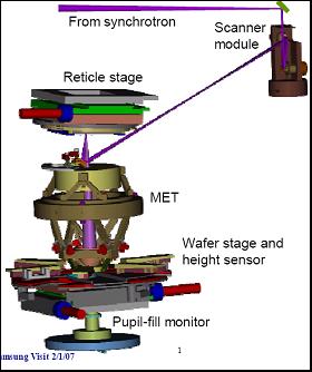
EUV Micro-Exposure Tool (MET) for Near-Term Development Using a High NA Projection System
 for Near-Term Development Using a High NA Projection System") EUV Micro-Exposure Tool (MET) for Near-Term Development Using a High NA Projection System John S. Taylor, Donald Sweeney, Russell Hudyma Layton Hale, Todd Decker Lawrence Livermore National Laboratory
EUV Micro-Exposure Tool (MET) for Near-Term Development Using a High NA Projection System John S. Taylor, Donald Sweeney, Russell Hudyma Layton Hale, Todd Decker Lawrence Livermore National Laboratory
Key Challenges in EUV Mask Technology: Actinic Mask Inspection and Mask 3D Effects. Yow-Gwo Wang
 Key Challenges in EUV Mask Technology: Actinic Mask Inspection and Mask 3D Effects by Yow-Gwo Wang A dissertation submitted in partial satisfaction of the requirements for the degree of Doctor of Philosophy
Lecture 8. Microlithography
 Lecture 8 Microlithography Lithography Introduction Process Flow Wafer Exposure Systems Masks Resists State of the Art Lithography Next Generation Lithography (NGL) Recommended videos: http://www.youtube.com/user/asmlcompany#p/search/1/jh6urfqt_d4
Opto-Mechanical Equipment of KBTEM: Present Day and the Future
 KBTEM JSC, Minsk, Belarus Opto-Mechanical Equipment of KBTEM: Present Day and the Future Quality Management System Certificate ISO-9001 since 2001 SPIE Member since 2003 www.kb-omo.by Dr. S.Avakaw SEMI
Performance data of a new 248 nm CD metrology tool proved on COG reticles and PSM s
 Performance data of a new 248 nm CD metrology tool proved on COG reticles and PSM s Gerhard Schlueter a, Walter Steinberg a, John Whittey b a Leica Microsystems Wetzlar GmbH Ernst-Leitz-Str. 17-37, D-35578
Major Fabrication Steps in MOS Process Flow
 Major Fabrication Steps in MOS Process Flow UV light Mask oxygen Silicon dioxide photoresist exposed photoresist oxide Silicon substrate Oxidation (Field oxide) Photoresist Coating Mask-Wafer Alignment
Immersion Lithography: New Opportunities for Semiconductor Manufacturing
 Immersion Lithography: New Opportunities for Semiconductor Manufacturing Tim Brunner, Dario Gil, Carlos Fonseca and Nakgeuon Seong IBM - SRDC Bob Streefkerk, Christian Wagner and Marco Stavenga ASML Outline
EUVL: Challenges to Manufacturing Insertion
 EUVL: Challenges to Manufacturing Insertion Obert R Wood II International Workshop on EUV Lithography CXRO, LBNL, Berkeley, California 14 June 2017 EUV Critical Issues List EUV Critical Issues, as identified
Optical Characterization and Defect Inspection for 3D Stacked IC Technology
 Minapad 2014, May 21 22th, Grenoble; France Optical Characterization and Defect Inspection for 3D Stacked IC Technology J.Ph.Piel, G.Fresquet, S.Perrot, Y.Randle, D.Lebellego, S.Petitgrand, G.Ribette FOGALE
Characterization of Actinic Mask Blank Inspection for Improving Sensitivity
 Characterization of Actinic Mask Blank Inspection for Improving Sensitivity Yoshihiro Tezuka, Toshihiko Tanaka, Tsuneo Terasawa, Toshihisa Tomie * M-ASET, Tsukuba, Japan * M-ASRC, AIST, Tsukuba, Japan
A process for, and optical performance of, a low cost Wire Grid Polarizer
 1.0 Introduction A process for, and optical performance of, a low cost Wire Grid Polarizer M.P.C.Watts, M. Little, E. Egan, A. Hochbaum, Chad Jones, S. Stephansen Agoura Technology Low angle shadowed deposition
INTERNATIONAL TECHNOLOGY ROADMAP LITHOGRAPHY FOR SEMICONDUCTORS 2009 EDITION
 INTERNATIONAL TECHNOLOGY ROADMAP FOR SEMICONDUCTORS 2009 EDITION LITHOGRAPHY THE ITRS IS DEVISED AND INTENDED FOR TECHNOLOGY ASSESSMENT ONLY AND IS WITHOUT REGARD TO ANY COMMERCIAL CONSIDERATIONS PERTAINING
TSMC Property. EUV Lithography. The March toward HVM. Anthony Yen. 9 September TSMC, Ltd
 EUV Lithography The March toward HVM Anthony Yen 9 September 2016 1 1 st EUV lithography setup and results, 1986 Si Stencil Mask SR W/C Multilayer Coating Optics λ=11 nm, provided by synchrotron radiation
Optics for EUV Lithography
 Optics for EUV Lithography Dr. Sascha Migura, Carl Zeiss SMT GmbH, Oberkochen, Germany 2018 EUVL Workshop June 13 th, 2018 Berkeley, CA, USA The resolution of the optical system determines the minimum
Lithography Simulation Tools Needed for 22nm HP and Beyond. Chris Mack
 Lithography Simulation Tools Needed for 22nm HP and Beyond Chris Mack www.lithoguru.com Slicing the Pie Simulation Tool Characteristics Precision Accuracy Capabilities (speed, features) Simulation Tool
Scaling of Semiconductor Integrated Circuits and EUV Lithography
 Scaling of Semiconductor Integrated Circuits and EUV Lithography ( 半導体集積回路の微細化と EUV リソグラフィー ) December 13, 2016 EIDEC (Emerging nano process Infrastructure Development Center, Inc.) Hidemi Ishiuchi 1 OUTLINE
Akira Miyake, Chidane Ouchi, International EUVL Symposium, October , Kobe Slide 1
 Development Status of Canon s EUVL Exposure Tool Akira Miyake, Chidane Ouchi, Hideki Morishima, and Hiroyoshi Kubo Canon Inc. International EUVL Symposium, October 18 2010, Kobe Slide 1 Outline EUVL Exposure
From ArF Immersion to EUV Lithography
 From ArF Immersion to EUV Lithography Luc Van den hove Vice President IMEC Outline Introduction 193nm immersion lithography EUV lithography Global collaboration Conclusions Lithography is enabling 1000
22nm node imaging and beyond: a comparison of EUV and ArFi double patterning
 22nm node imaging and beyond: a comparison of EUV and ArFi double patterning ASML: Eelco van Setten, Orion Mouraille, Friso Wittebrood, Mircea Dusa, Koen van Ingen-Schenau, Jo Finders, Kees Feenstra IMEC:
Inspection of templates for imprint lithography
 Inspection of templates for imprint lithography Harald F. Hess, a) Don Pettibone, David Adler, and Kirk Bertsche KLA-Tencor 160 Rio Robles, San Jose, California 95134 Kevin J. Nordquist, David P. Mancini,
Shot noise and process window study for printing small contacts using EUVL. Sang Hun Lee John Bjorkohlm Robert Bristol
 Shot noise and process window study for printing small contacts using EUVL Sang Hun Lee John Bjorkohlm Robert Bristol Abstract There are two issues in printing small contacts with EUV lithography (EUVL).
PicoMaster 100. Unprecedented finesse in creating 3D micro structures. UV direct laser writer for maskless lithography
 UV direct laser writer for maskless lithography Unprecedented finesse in creating 3D micro structures Highest resolution in the market utilizing a 405 nm diode laser Structures as small as 300 nm 375 nm
Imaging for the next decade
 Imaging for the next decade Martin van den Brink Executive Vice President Products & Technology IMEC Technology Forum 2009 3 June, 2009 Slide 1 Congratulations! ASML and years of making chips better Slide
Multi-beam mask writer MBM-1000 for advanced mask making
 Multi-beam mask writer MBM-1000 for advanced mask making H. Matsumoto NuFlare Technology, Inc. Slide 1 Multi-beam Shaping aperture array (SAA) Blanking aperture array (BAA) Sub deflectors Main deflectors