EUVL Challenges for Next Generation Devices
|
|
|
- Warren Poole
- 5 years ago
- Views:
Transcription

1 EUVL Challenges for Next Generation Devices Center for Semiconductor Research & Development Advanced Lithography Process Technology Dept. Tatsuhiko Higashiki
2 Contents Device Roadmap and Lithography Extendibility toward 1x nm hp and beyond with New Lithography SAxP EUVL EUVL+DSA Conclusion 2
3 Contents Device Roadmap and Lithography Extendibility toward 1x nm hp and beyond with New Lithography SAxP EUVL EUVL+DSA Conclusion 3

4 Rapid Increase of Information Volume Demand All information that is created, captured, replicated and/or consumed by all human on the planet. 40ZB 1ZB=1,000,000,000,000,000,000,000=10^21B 20ZB All information is not fully stored, but partially stored. Need for larger-capacity memory in the future. 4
5 5


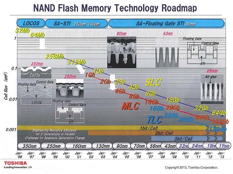
6 Roadmap of the Memory CG CG CG STI FG FG FG FG STI FG FG FG STI FG FG FG NAND BiCS Cross Point 6
7 More than Moore Lithography Challenges ArF im NA>1~1.35 Light Source EUVL NA0.32 >0.4x? ArF im SADP More Moore hp56nm hp43nm hp32nm hp2xnm hp1xnm hp0xnm Tool Defect ML2 NIL Resist, Mask, Inspection, etc Cost EUVL+SADP EUVL+DSA ArF imsaqp/saop? Arf im SAQP+DSA NIL+DSA Performance & Economics ML2+DSA SADP : self-aligned double patterning SAQP : self-aligned quadruple patterning SAOP : self-aligned octuplet patterning 7
8 Contents Device Roadmap and Lithography Extendibility toward 1x nm hp and beyond with New Lithography SAxP EUVL EUVL+DSA Conclusion 8
9 More than Moore Lithography Challenges ArF im NA>1~1.35 Light Source EUVL NA0.32 >0.4x? ArF im SADP More Moore hp56nm hp43nm hp32nm hp2xnm hp1xnm hp0xnm Tool Defect ML2 NIL Resist, Mask, Inspection, etc Cost EUVL+SADP EUVL+DSA ArF imsaqp/saop? Arf im SAQP+DSA NIL+DSA Performance & Economics ML2+DSA SADP : self-aligned double patterning SAQP : self-aligned quadruple patterning SAOP : self-aligned octuplet patterning 9
 EUVL")

10 Single Exposure by Mask Technology Revolution SADP Mask (Template) EUVL single single Litho. Exposed Slimming Film depo. etching etching Processed 10


 Mask Cost Opportunity Cost ( Time is money")
11 CoO ( /wf) CoO ( /wf) Cycle time can not be described on CoO Single Exposure DPT Patterning Δ Cycle time Patterning Cycle time DPT Economical Problems Investment Cost (LP, Etching, M&I, etc.) Mask Cost Opportunity Cost ( Time is money ) Ref T.Higashiki ConFab2010(June) 11
12 Contents Device Roadmap and Lithography Extendibility toward 1x nm hp and beyond with New Lithography SAxP EUVL EUVL+DSA Conclusion 12
13 More than Moore Lithography Challenges ArF im NA>1~1.35 Light Source EUVL NA0.32 >0.4x? ArF im SADP More Moore hp56nm hp43nm hp32nm hp2xnm hp1xnm hp0xnm Tool Defect ML2 NIL Resist, Mask, Inspection, etc Cost EUVL+SADP EUVL+DSA ArF imsaqp/saop? Arf im SAQP+DSA NIL+DSA Performance & Economics ML2+DSA SADP : self-aligned double patterning SAQP : self-aligned quadruple patterning SAOP : self-aligned octuplet patterning 13
14 EUVL Challenges for NAND Memory Mask Defect Control DD<0.1/cm2 Inspection ABI(Actinic Blanks Inspection) PI(Pattern Inspection) Inspection after Pattern Repairing Resist Performance Resolution<hp16nm,LWR<2nm,Photo Speed<20mj/cm2,Difectivity<0.1/cm2 Light Source Performance Enough Power for Throughput>150wph Operational Cost (Mirror, E Power, DMT, etc) 14
15 Ref, EIDEC Symposium
16 EUV Collaboration Device & design Si Process Lithography Pattern Layout Tech. (OPC/DFM) Specification Design for Tools Mask process Resist process Advanced EUVL Mask Quality Mask Inspections Resist Quality High NA Exposure EUVL+DSA Suppliers Exposure Tool EDA Resist Material Mask Metrology and Inspection 16

17 Structure of EUVL Mask EUV Mask Section and Defects Absorber Reflective Multilayer Phase Defect Pattern Defect Damage after repairing Ref T.Higashiki ConFab2010(June) 17

18 Ref H.Watanabe, EIDEC Symposium

 Stepping (X)")
19 EB inspection tool Detector Electron Gun EUV Mask EUV Mask Detector: TDI Sensor Electron Gun Projection Electron Microscope EBeyeM EUV Mask Continuous Moving (Y) Stepping (X) 19


20 Quality assurance of hotspot & repaired pattern EUV AIMS operation will be difficult in D SEM + Litho. Simulation will be applied. -5deg top-down +5deg Top-down & tilted SEM images of mask pattern Prediction of wafer image 3D mask image Lithography simulation 20
21 Toshiba Technology Scenario for EUV Mask Multilayer defect inspection Patterned mask inspection Defect repair HP 2Xnm DUV inspection DUV inspection EB repair HP 1Xnm Actinic inspection EB inspection Hotspot & repaired pattern assurance Particle inspection Litho. Sim. w/ 3D mask image EB inspection ready under developing EUV-AIMS 21


 CDU of 44nm (4x) L&S :")
 Developing Area Cross-sectional view Gap Mask Extreme high uniformity of developing")
22 Rinse Suction Developing Solution Suction Rinse EB writer : EBM8000 (NuFlare) Absorber Pattern Generation Scanning-type Developer : PGSD Proximity-Gap-Suction-Development System (Tokyo Electron) Scan Dry Etching Equipment : ARES TM (Shibaura Mechatronics) product/ebm.html 44nm (4x) L&S Slit and scan type development Narrow gap Suction slits for removing dissolution products Scan Mask Mask Stage PGSD Nozzle TaBO TaBN Ru 90(deg) CDU of 44nm (4x) L&S : 1.7nm (3sigma) Gap Sensor Iino, et al. (BACUS2010) Developing Area Cross-sectional view Gap Mask Extreme high uniformity of developing solution supply Nearly zero loading effect caused by dissolution products Etched absorber pattern has capability for scaling down to hp1x EUVL single exposure. 22

23 SMRAT Network of Mask & Lithography Toshiba R&D Center DTF Mask House (EUVL Infrastructure Development Center) Mask Inspections High Performance Resist Sub-10nm DSA material EB Writer Inspection Cleaning Tech. Etching Toshiba Advanced Litho.& Mask Dept. Advance Mask & Litho Computational Litho OPC/DFM Next Emerging Litho. Toshiba Confidential 23


24 Resolution Limit of EUVL Depend on Resist Performance 24


25 EUVL and SADP Complementally dteos 加工後 hp14nm Exposure was Realized by EUVL + SADP EUVL Resist 28nm Spacer Film 14nm Si ウェハ hp28nm Spacer hp14nm Y. Watanabe et al, Photomask Japan 2010(April) 25
26 Contents Device Roadmap and Lithography Extendibility toward 1x nm hp and beyond with New Lithography SAxP EUVL EUVL+DSA Conclusion 26
27 More than Moore Lithography Challenges ArF im NA>1~1.35 Light Source EUVL NA0.32 >0.4x? ArF im SADP More Moore hp56nm hp43nm hp32nm hp2xnm hp1xnm hp0xnm Tool Defect ML2 NIL Resist, Mask, Inspection, etc Cost EUVL+SADP EUVL+DSA ArF imsaqp/saop? Arf im SAQP+DSA NIL+DSA Performance & Economics ML2+DSA SADP : self-aligned double patterning SAQP : self-aligned quadruple patterning SAOP : self-aligned octuplet patterning 27
 Specification Design for Tools Mask process Resist process")

28 EUV Collaboration Device & design Si Process Lithography Pattern Layout Tech. (OPC/DFM) Specification Design for Tools Mask process Resist process Advanced EUVL Mask Quality Mask Inspections Resist Quality High NA Exposure EUVL+DSA Suppliers Exposure Tool EDA Resist Material Mask Metrology and Inspection 28
29 DSA(Directed Self Assembly) Change in Size Molecular Weight B polymer Spherical Cylindrical Bicontinuos Lamella A polymer Composition Change in Structure Hydrophilic Hydrophobic Chemical bond DSA Molecule Micro-Phase Separated Structures of Block-copolymer K. Asakawa, T. Hiraoka, Jpn. J. Appl. Phys. vol.41, 6112 (2002). 29
 Hydrophilic")

30 DSA (Directed Self Assembly) Hydrophobic (PS) Hydrophilic (PMMA) BCP: Block copolymer Line & Space Contact Hole 30
 Nato et al.")
 Chen et al.")
 Tada, Macromol.")
31 Grapho-Epitaxy & Chemo-Epitaxy Segalmann et al., Adv.Mater. 3,1152(2001) Nato et al., IEEE Trans. Magn.38,1949(2002) Chen et al.,appl.phys.lett.81,3657(2002) Chen et al.,adv.mater. 20,3155(2008) Rulz et al., Science, 321,936(2008) Tada, Macromol.41,9267(2008) 31


32 Guide Hole vs. DSA Hole Guide hole DSA hole Ave. CD 72.1nm Ave. CD 28.5nm 3sigma 7.6nm 3sigma 1.3nm Ref.Y.Seino, SPIE Advanced Lithography


33 DSA OPC/DfM/APC Flow OPC EDA Tool DfM Model Condition (material/process) APC Layout Guide Data OPC Litho Simulation GDS DSA Simulation HotSpot result Judge Wafer Process FeedBack EDA Tool FeedForward 33
 Target (5nm) TAT (?")

34 Prediction Accuracy DSA Simulation Model Shroedinger's Equation etc Rigorous Model Impractical model (<0.25nm) Target (5nm) TAT (? years/10μm2) SCF DPD TAT (5h/10μm2) TAT (1m/10μm2) speed Model Self Consistent mean Field Dissipative Particle Dynamics methodology Based on statistical field theory Challenge Modeling of thermal fluctuations Based on Newton's motion equation Difficult to fit to a measured data 34


")


35 Molecular Dynamics based DSA Simulation Model Coarse Grained MD DPD(Dissipative Particle Dynamics) Coarse Graining Available Free Software Tools are; LAMMPS /GROMAX/ OCTA-COGNAC,, Dissipative Force Brownian Motion Repulsive Force Solvent Δvelocity Beads Spring Spring Force 35
36 Challenges for DSA Lithography High performance DSA material High χ material Resolution, LWR/LER, Etching Long term stability Robust material and tool for environmental control such as surface energy stability, temperature, humidity, pressure and PH, etc. Defectivity, CD and overlay accuracy Development of molecular dynamics based DSA simulator More accurate simulation model BCP and related molecular design Microphase separation (2D/3D) TAT / accuracy trade-off DSA OPC/DFM technology Design rule verification DSA and guide patterning (litho/wet/dry) Metrology & Inspection Metrology for 3D profile Inspection technology for 1xnmhp and beyond needs to overcome throughput / accuracy / sensitivity trade-off. 36
37 Contents Device Roadmap and Lithography Extendibility toward 1x nm hp and beyond with New Lithography SAxP EUVL EUVL+DSA Conclusion 37
38 Conclusion Economical factor is dominant criteria for a lithography strategy For Memory Device; Throughput, Investment & Si Process Cost For Logic Device ; Mask Cost, Cycle Time EUVL Moving from R&D phase to production Light source performance is improving, but a significant concern. DSA DSA will be a complementary technology for all other lithography EUVL+DSA will be one of candidates for sub 10nm lithography. Next Challenges Next generation lithography will depend on innovation of infrastructure technologies such as OPC, DFM, M&I, etching and cleaning. 38


39 2013/7/7 39
5 th Annual ebeam Initiative Luncheon SPIE February 26, Aki Fujimura CEO D2S, Inc. Managing Company Sponsor ebeam Initiative
 5 th Annual ebeam Initiative Luncheon SPIE February 26, 2013 Aki Fujimura CEO D2S, Inc. Managing Company Sponsor ebeam Initiative ebeam Writes All Chips The ebeam Initiative: Is an educational platform
2009 International Workshop on EUV Lithography
 Contents Introduction Absorber Stack Optimization Non-flatness Correction Blank Defect and Its Mitigation Wafer Printing Inspection Actinic Metrology Cleaning and Repair Status Remaining Issues in EUV
Progresses in NIL Template Fabrication Naoya Hayashi
 Progresses in NIL Template Fabrication Naoya Hayashi Electronic Device Operations Dai Nippon Printing Co., Ltd. Contents 1. Introduction Motivation NIL mask fabrication process 2. NIL mask resolution improvement
Holistic View of Lithography for Double Patterning. Skip Miller ASML
 Holistic View of Lithography for Double Patterning Skip Miller ASML Outline Lithography Requirements ASML Holistic Lithography Solutions Conclusions Slide 2 Shrink Continues Lithography keeps adding value
Lithography. Development of High-Quality Attenuated Phase-Shift Masks
 Lithography S P E C I A L Development of High-Quality Attenuated Phase-Shift Masks by Toshihiro Ii and Masao Otaki, Toppan Printing Co., Ltd. Along with the year-by-year acceleration of semiconductor device
Challenges of EUV masks and preliminary evaluation
 Challenges of EUV masks and preliminary evaluation Naoya Hayashi Electronic Device Laboratory Dai Nippon Printing Co.,Ltd. EUV Mask Workshop 2004 1 Contents Recent Lithography Options on Roadmap Challenges
(Complementary E-Beam Lithography)
") Extending Optical Lithography with C E B L (Complementary E-Beam Lithography) July 13, 2011 4008 Burton Drive, Santa Clara, CA 95054 Outline Complementary Lithography E-Beam Complements Optical Multibeam
Extending Optical Lithography with C E B L (Complementary E-Beam Lithography) July 13, 2011 4008 Burton Drive, Santa Clara, CA 95054 Outline Complementary Lithography E-Beam Complements Optical Multibeam
A Study of Wafer Plane Analysis with Mask MVM-SEM using 2D and 3D Images
 A Study of Wafer Plane Analysis with Mask MVM-SEM using 2D and 3D Images Takayuki Nakamura ADVANTEST CORPORATION February 24, 2015 San Jose, California Member 2015/2/20 All Rights Reserved - ADVANTEST
Light Sources for EUV Mask Metrology. Heiko Feldmann, Ulrich Müller
 Light Sources for EUV Mask Metrology Heiko Feldmann, Ulrich Müller Dublin, October 9, 2012 Agenda 1 2 3 4 Actinic Metrology in Mask Making The AIMS EUV Concept Metrology Performance Drivers and their Relation
Mask Technology Development in Extreme-Ultraviolet Lithography
 Mask Technology Development in Extreme-Ultraviolet Lithography Anthony Yen September 6, 2013 Projected End of Optical Lithography 2013 TSMC, Ltd 1976 1979 1982 1985 1988 1991 1994 1997 2000 2003 2007 2012
Advanced Patterning Techniques for 22nm HP and beyond
 Advanced Patterning Techniques for 22nm HP and beyond An Overview IEEE LEOS (Bay Area) Yashesh A. Shroff Intel Corporation Aug 4 th, 2009 Outline The Challenge Advanced (optical) lithography overview Flavors
UV Nanoimprint Stepper Technology: Status and Roadmap. S.V. Sreenivasan Sematech Litho Forum May 14 th, 2008
 UV Nanoimprint Stepper Technology: Status and Roadmap S.V. Sreenivasan Sematech Litho Forum May 14 th, 2008 Overview Introduction Stepper technology status: Patterning and CD Control Through Etch Alignment
Computational Lithography Requirements & Challenges for Mask Making. Naoya Hayashi, Dai Nippon Printing Co., Ltd
 Computational Lithography Requirements & Challenges for Mask Making Naoya Hayashi, Dai Nippon Printing Co., Ltd Contents Introduction Lithography Trends Computational lithography options More Complex OPC
Recent Activities of the Actinic Mask Inspection using the EUV microscope at Center for EUVL
 Recent Activities of the Actinic Mask Inspection using the EUV microscope at Center for EUVL Takeo Watanabe, Tetsuo Harada, and Hiroo Kinoshita Center for EUVL, University of Hyogo Outline 1) EUV actinic
Process Optimization
 Process Optimization Process Flow for non-critical layer optimization START Find the swing curve for the desired resist thickness. Determine the resist thickness (spin speed) from the swing curve and find
DSA and 193 immersion lithography
 NIKON RESEARCH CORP. OF AMERICA DSA and 193 immersion lithography Steve Renwick Senior Research Scientist, Imaging Sol ns Technology Development Where the industry wants to go 2 Where we are now 193i e-beam
Optical Microlithography XXVIII
 PROCEEDINGS OF SPIE Optical Microlithography XXVIII Kafai Lai Andreas Erdmann Editors 24-26 February 2015 San Jose, California, United States Sponsored by SPIE Cosponsored by Cymer, an ASML company (United
PUSHING LITHOGRAPHY TO ENABLE ULTIMATE NANO-ELECTRONICS. LUC VAN DEN HOVE President & CEO imec
 PUSHING LITHOGRAPHY TO ENABLE ULTIMATE NANO-ELECTRONICS LUC VAN DEN HOVE President & CEO imec OUTLINE! Industry drivers! Roadmap extension! Lithography options! Innovation through global collaboration
EUVL getting ready for volume introduction
 EUVL getting ready for volume introduction SEMICON West 2010 Hans Meiling, July 14, 2010 Slide 1 public Outline ASML s Lithography roadmap to support Moore s Law Progress on 0.25NA EUV systems Progress
TECHNOLOGY ROADMAP 2011 EDITION LITHOGRAPHY FOR
 INTERNATIONAL TECHNOLOGY ROADMAP FOR SEMICONDUCTORS 2011 EDITION LITHOGRAPHY THE ITRS IS DEVISED AND INTENDED FOR TECHNOLOGY ASSESSMENT ONLY AND IS WITHOUT REGARD TO ANY COMMERCIAL CONSIDERATIONS PERTAINING
Actinic Review of EUV Masks: Performance Data and Status of the AIMS TM EUV System
 Actinic Review of EUV Masks: Performance Data and Status of the AIMS TM EUV System Dirk Hellweg*, Markus Koch, Sascha Perlitz, Martin Dietzel, Renzo Capelli Carl Zeiss SMT GmbH, Rudolf-Eber-Str. 2, 73447
Update on 193nm immersion exposure tool
 Update on 193nm immersion exposure tool S. Owa, H. Nagasaka, Y. Ishii Nikon Corporation O. Hirakawa and T. Yamamoto Tokyo Electron Kyushu Ltd. January 28, 2004 Litho Forum 1 What is immersion lithography?
Shooting for the 22nm Lithography Goal with the. Coat/Develop Track. SOKUDO Lithography Breakfast Forum 2010 July 14 (L1)
") Shooting for the 22nm Lithography Goal with the Coat/Develop Track SOKUDO Lithography Breakfast Forum 2010 July 14 (L1) Three (3) different exposure options for 22nm: Public External (L1) MAPPER Lithography
Shooting for the 22nm Lithography Goal with the Coat/Develop Track SOKUDO Lithography Breakfast Forum 2010 July 14 (L1) Three (3) different exposure options for 22nm: Public External (L1) MAPPER Lithography
Toward 5nm node ; Untoward Scaling with Multi-patterning
 1 st International Symposium on DSA Toward 5nm node ; Untoward Scaling with Multi-patterning 27 th OCT 2015 H. Yaegashi Chief Engineer Tokyo Electron Limited Down-caling trend towards N5 N20 N14 N10 N7
Section 2: Lithography. Jaeger Chapter 2 Litho Reader. The lithographic process
 Section 2: Lithography Jaeger Chapter 2 Litho Reader The lithographic process Photolithographic Process (a) (b) (c) (d) (e) (f) (g) Substrate covered with silicon dioxide barrier layer Positive photoresist
Scaling of Semiconductor Integrated Circuits and EUV Lithography
 Scaling of Semiconductor Integrated Circuits and EUV Lithography ( 半導体集積回路の微細化と EUV リソグラフィー ) December 13, 2016 EIDEC (Emerging nano process Infrastructure Development Center, Inc.) Hidemi Ishiuchi 1 OUTLINE
Section 2: Lithography. Jaeger Chapter 2 Litho Reader. EE143 Ali Javey Slide 5-1
 Section 2: Lithography Jaeger Chapter 2 Litho Reader EE143 Ali Javey Slide 5-1 The lithographic process EE143 Ali Javey Slide 5-2 Photolithographic Process (a) (b) (c) (d) (e) (f) (g) Substrate covered
Evaluation of Technology Options by Lithography Simulation
 Evaluation of Technology Options by Lithography Simulation Andreas Erdmann Fraunhofer IISB, Erlangen, Germany Semicon Europe, Dresden, October 12, 2011 Outline Introduction: Resolution limits of optical
Lithography Industry Collaborations
 Accelerating the next technology revolution Lithography Industry Collaborations SOKUDO Breakfast July 13, 2011 Stefan Wurm SEMATECH Copyright 2009 SEMATECH, Inc. SEMATECH, and the SEMATECH logo are registered
Lithography Roadmap. without immersion lithography. Node Half pitch. 248nm. 193nm. 157nm EUVL. 3-year cycle: 2-year cycle: imec 2005
 Lithography Roadmap without immersion lithography Node Half pitch 180 nm 130 nm 90 nm 65 nm 45 nm 32 nm 22 nm 250 nm 180 nm 130 nm 90 nm 65 nm 45 nm 32 nm 248nm 193nm 157nm EUVL 3-year cycle: 2-year cycle:
Sub-12nm Optical Lithography with 4x Pitch Division and SMO-Lite
 Sub-12nm Optical Lithography with 4x Pitch Division and SMO-Lite Michael C. Smayling* a, Koichiro Tsujita b, Hidetami Yaegashi c, Valery Axelrad d Tadashi Arai b, Kenichi Oyama c, Arisa Hara c a Tela Innovations,
Optical Lithography. Keeho Kim Nano Team / R&D DongbuAnam Semi
 Optical Lithography Keeho Kim Nano Team / R&D DongbuAnam Semi Contents Lithography = Photolithography = Optical Lithography CD : Critical Dimension Resist Pattern after Development Exposure Contents Optical
Development of Nanoimprint Mold Using JBX-9300FS
 Development of Nanoimprint Mold Using JBX-9300FS Morihisa Hoga, Mikio Ishikawa, Naoko Kuwahara Tadahiko Takikawa and Shiho Sasaki Dai Nippon Printing Co., Ltd Research & Development Center Electronic Device
EUVL Activities in China. Xiangzhao Wang Shanghai Inst. Of Opt. and Fine Mech. Of CAS. (SIOM) Shanghai, China.
 Shanghai, China.") EUVL Activities in China Xiangzhao Wang Shanghai Inst. Of Opt. and Fine Mech. Of CAS. (SIOM) Shanghai, China. wxz26267@siom.ac.cn Projection Optics Imaging System Surface Testing Optical Machining ML Coating
EUVL Activities in China Xiangzhao Wang Shanghai Inst. Of Opt. and Fine Mech. Of CAS. (SIOM) Shanghai, China. wxz26267@siom.ac.cn Projection Optics Imaging System Surface Testing Optical Machining ML Coating
Registration performance on EUV masks using high-resolution registration metrology
 Registration performance on EUV masks using high-resolution registration metrology Steffen Steinert a, Hans-Michael Solowan a, Jinback Park b, Hakseung Han b, Dirk Beyer a, Thomas Scherübl a a Carl Zeiss
CD-SEM for 65-nm Process Node
 CD-SEM for 65-nm Process Node 140 CD-SEM for 65-nm Process Node Hiroki Kawada Hidetoshi Morokuma Sho Takami Mari Nozoe OVERVIEW: Inspection equipment for 90-nm and subsequent process nodes is required
IDeAL program : DSA activity at LETI. S. Tedesco R. Tiron L. Pain
 IDeAL program : DSA activity at LETI S. Tedesco R. Tiron L. Pain Outline Why DSA for microelectronics The IDeAL progam Graphoepitaxy of BCP Contact hole application 300 mm pilot line in LETI Conclusion
2008 European EUVL. EUV activities the EUVL shop future plans. Rob Hartman
 2008 European EUVL EUV activities the EUVL shop future plans Rob Hartman 2007 international EUVL Symposium 28-31 October 2007 2008 international EUVL Symposium 28 Sapporo, September Japan 1 October 2008
Photolithography. References: Introduction to Microlithography Thompson, Willson & Bowder, 1994
 Photolithography References: Introduction to Microlithography Thompson, Willson & Bowder, 1994 Microlithography, Science and Technology Sheats & Smith, 1998 Any other Microlithography or Photolithography
TWINSCAN XT:1950i Water-based immersion taken to the max Enabling fast, single-exposure lithography at sub 40 nm
 TWINSCAN XT:1950i Water-based immersion taken to the max Enabling fast, single-exposure lithography at sub 40 nm SEMICON West, San Francisco July 14-18, 2008 Slide 1 The immersion pool becomes an ocean
Electron Multi-Beam Technology for Mask and Wafer Direct Write. Elmar Platzgummer IMS Nanofabrication AG
 Electron Multi-Beam Technology for Mask and Wafer Direct Write Elmar Platzgummer IMS Nanofabrication AG Contents 2 Motivation for Multi-Beam Mask Writer (MBMW) MBMW Tool Principles and Architecture MBMW
SEMATECH Defect Printability Studies
 Accelerating the next technology revolution SEMATECH Defect Printability Studies Il Yong Jang 1, Jenah Harris-Jones 1, Ranganath Teki 1, Vibhu Jindal 1, Frank Goodwin 1 Masaki Satake 2, Ying Li 2, Danping
Progress in full field EUV lithography program at IMEC
 Progress in full field EUV lithography program at IMEC A.M. Goethals*, G.F. Lorusso*, R. Jonckheere*, B. Baudemprez*, J. Hermans*, F. Iwamoto 1, B.S. Kim 2, I.S. Kim 2, A. Myers 3, A. Niroomand 4, N. Stepanenko
immersion optics Immersion Lithography with ASML HydroLith TWINSCAN System Modifications for Immersion Lithography by Bob Streefkerk
 immersion optics Immersion Lithography with ASML HydroLith by Bob Streefkerk For more than 25 years, many in the semiconductor industry have predicted the end of optical lithography. Recent developments,
Present Status and Future Prospects of EUV Lithography
 3rd EUV-FEL Workshop Present Status and Future Prospects of EUV Lithography (EUV リソグラフィーの現状と将来展望 ) December 11, 2011 Evolving nano process Infrastructure Development Center, Inc. (EIDEC) Hidemi Ishiuchi
Multiple Patterning for Immersion Extension and EUV Insertion. Chris Bencher Distinguished Member of Technical Staff Applied Materials CTO group
 Multiple Patterning for Immersion Extension and EUV Insertion Chris Bencher Distinguished Member of Technical Staff Applied Materials CTO group Abstract Multiple Patterning for Immersion Extension and
Defect printability of thin absorber mask in EUV lithography with refined LER resist
 [#5, MA] Defect printability of thin absorber mask in EUV lithography with refined LER resist Takashi Kamo, Hajime Aoyama, Yukiyasu Arisawa, Mihoko Kijima, Toshihiko Tanaka and Osamu Suga e-mail: kamo.takashi@selete.co.jp
Photolithography Technology and Application
 Photolithography Technology and Application Jeff Tsai Director, Graduate Institute of Electro-Optical Engineering Tatung University Art or Science? Lind width = 100 to 5 micron meter!! Resolution = ~ 3
Status and challenges of EUV Lithography
 Status and challenges of EUV Lithography SEMICON Europa Dresden, Germany Jan-Willem van der Horst Product Manager EUV October 10 th, 2013 Slide 2 Contents Introduction NXE:3100 NXE:3300B Summary and acknowledgements
Imec pushes the limits of EUV lithography single exposure for future logic and memory
 Edition March 2018 Semiconductor technology & processing Imec pushes the limits of EUV lithography single exposure for future logic and memory Imec has made considerable progress towards enabling extreme
Development of ultra-fine structure t metrology system using coherent EUV source
 2009 International Workshop On EUV Lithography, July 13-17,2009 Development of ultra-fine structure t metrology system using coherent EUV source University of Hyogo 1, Hiroo Kinoshita 1,3, Tetuo Harada
Shot noise and process window study for printing small contacts using EUVL. Sang Hun Lee John Bjorkohlm Robert Bristol
 Shot noise and process window study for printing small contacts using EUVL Sang Hun Lee John Bjorkohlm Robert Bristol Abstract There are two issues in printing small contacts with EUV lithography (EUVL).
450mm patterning out of darkness Backend Process Exposure Tool SOKUDO Lithography Breakfast Forum July 10, 2013 Doug Shelton Canon USA Inc.
 450mm patterning out of darkness Backend Process Exposure Tool SOKUDO Lithography Breakfast Forum 2013 July 10, 2013 Doug Shelton Canon USA Inc. Introduction Half Pitch [nm] 2013 2014 2015 2016 2017 2018
Copyright 2000, Society of Photo-Optical Instrumentation Engineers This paper was published in Optical Microlithography XIII, Volume 4000 and is made
 Copyright 00, Society of Photo-Optical Instrumentation Engineers This paper was published in Optical Microlithography XIII, Volume 4000 and is made available as an electronic reprint with permission of
Major Fabrication Steps in MOS Process Flow
 Major Fabrication Steps in MOS Process Flow UV light Mask oxygen Silicon dioxide photoresist exposed photoresist oxide Silicon substrate Oxidation (Field oxide) Photoresist Coating Mask-Wafer Alignment
Section 2: Lithography. Jaeger Chapter 2. EE143 Ali Javey Slide 5-1
 Section 2: Lithography Jaeger Chapter 2 EE143 Ali Javey Slide 5-1 The lithographic process EE143 Ali Javey Slide 5-2 Photolithographic Process (a) (b) (c) (d) (e) (f) (g) Substrate covered with silicon
Recent Development Activities on EUVL at ASET
 Title Recent Development Activities on at ASET Shinji Okazaki ASET Laboratory 2 nd International Workshop on 1 Overall Development Plan 98 99 00 01 02 03 04 05 06 07 08 ASET Basic Technologies 100% Government
INTERNATIONAL TECHNOLOGY ROADMAP SEMICONDUCTORS 2001 EDITION LITHOGRAPHY FOR
 INTERNATIONAL TECHNOLOGY ROADMAP FOR SEMICONDUCTORS 2001 EDITION LITHOGRAPHY TABLE OF CONTENTS Scope...1 Difficult Challenges...1 Lithography Technology Requirements...3 Potential Solutions...14 Crosscut
Novel EUV Resist Development for Sub-14nm Half Pitch
 EUV Workshop 2015 Maui, HI P64 Novel EUV Resist Development for Sub-14nm Half Pitch Yoshi Hishiro JSR Micro Inc. EUV Workshop, June 17, 2015 1 Contents Requirement for sub-14nm HP EUV resist JSR strategy
Photolithography I ( Part 1 )
") 1 Photolithography I ( Part 1 ) Chapter 13 : Semiconductor Manufacturing Technology by M. Quirk & J. Serda Bjørn-Ove Fimland, Department of Electronics and Telecommunication, Norwegian University of Science
1 Photolithography I ( Part 1 ) Chapter 13 : Semiconductor Manufacturing Technology by M. Quirk & J. Serda Bjørn-Ove Fimland, Department of Electronics and Telecommunication, Norwegian University of Science
EUV Actinic Blank Inspection Tool Development
 EUV Actinic Blank Inspection Tool Development EUVL Symposium 2011 Hiroki Miyai 1, Tomohiro Suzuki 1, Kiwamu Takehisa 1, Haruhiko Kusunose 1, Takeshi Yamane 2, Tsuneo Terasawa 2, Hidehiro Watanabe 2, Soichi
EUVL Scanners Operational at Chipmakers. Skip Miller Semicon West 2011
 EUVL Scanners Operational at Chipmakers Skip Miller Semicon West 2011 Outline ASML s Lithography roadmap to support Moore s Law Progress on NXE:3100 (0.25NA) EUV systems Progress on NXE:3300 (0.33NA) EUV
PHGN/CHEN/MLGN 435/535: Interdisciplinary Silicon Processing Laboratory. Simple Si solar Cell!
 Where were we? Simple Si solar Cell! Two Levels of Masks - photoresist, alignment Etch and oxidation to isolate thermal oxide, deposited oxide, wet etching, dry etching, isolation schemes Doping - diffusion/ion
Mask Fabrication For Nanoimprint Lithography
 Mask Fabrication For Nanoimprint Lithography Doug Resnick Canon Nanotechnologies 1807C W. Braker Lane Austin, TX 78758 * dresnick@cnt.canon.com Template (Imprint Mask) Fabrication: Outline E-beam and Etch
Imaging for the next decade
 Imaging for the next decade Martin van den Brink Executive Vice President Products & Technology IMEC Technology Forum 2009 3 June, 2009 Slide 1 Congratulations! ASML and years of making chips better Slide
R&D Status and Key Technical and Implementation Challenges for EUV HVM
 R&D Status and Key Technical and Implementation Challenges for EUV HVM Sam Intel Corporation Agenda Requirements by Process Node EUV Technology Status and Gaps Photoresists Tools Reticles Summary 2 Moore
AOARD REPORT The Photomask Japan '94 Held 22 April 94 at Kawasaki Science Park, Kanagawa, Japan
 > AOARD-TR-94-22 AOARD REPORT The Photomask Japan '94 Held 22 April 94 at Kawasaki Science Park, Kanagawa, Japan 22 April 1994 S. J. Yakura AOARD The Photomask Japan '94 symposium, the first photomask
MICROCHIP MANUFACTURING by S. Wolf
 MICROCHIP MANUFACTURING by S. Wolf Chapter 19 LITHOGRAPHY II: IMAGE-FORMATION and OPTICAL HARDWARE 2004 by LATTICE PRESS CHAPTER 19 - CONTENTS Preliminaries: Wave- Motion & The Behavior of Light Resolution
Benefit of ArF immersion lithography in 55 nm logic device manufacturing
 Benefit of ArF immersion lithography in 55 nm logic device manufacturing Takayuki Uchiyama* a, Takao Tamura a, Kazuyuki Yoshimochi a, Paul Graupner b, Hans Bakker c, Eelco van Setten c, Kenji Morisaki
5. Lithography. 1. photolithography intro: overall, clean room 2. principle 3. tools 4. pattern transfer 5. resolution 6. next-gen
 5. Lithography 1. photolithography intro: overall, clean room 2. principle 3. tools 4. pattern transfer 5. resolution 6. next-gen References: Semiconductor Devices: Physics and Technology. 2 nd Ed. SM
Scope and Limit of Lithography to the End of Moore s Law
 Scope and Limit of Lithography to the End of Moore s Law Burn J. Lin tsmc, Inc. 1 What dictate the end of Moore s Law Economy Device limits Lithography limits 2 Litho Requirement of Critical Layers Logic
Semiconductor Manufacturing Technology. Semiconductor Manufacturing Technology. Photolithography: Resist Development and Advanced Lithography
 Semiconductor Manufacturing Technology Michael Quirk & Julian Serda October 2001 by Prentice Hall Chapter 15 Photolithography: Resist Development and Advanced Lithography Eight Basic Steps of Photolithography
TSMC Property. EUV Lithography. The March toward HVM. Anthony Yen. 9 September TSMC, Ltd
 EUV Lithography The March toward HVM Anthony Yen 9 September 2016 1 1 st EUV lithography setup and results, 1986 Si Stencil Mask SR W/C Multilayer Coating Optics λ=11 nm, provided by synchrotron radiation
The Coherent EUV Scatterometry Microscope for Actinic Mask Inspection and Metrology
 The Coherent EUV Scatterometry Microscope for Actinic Mask Inspection and Metrology Tetsuo Harada* 1,3, Masato Nakasuji 1,3, Teruhiko Kimura 1,3, Yutaka Nagata 2,3, Takeo Watanabe 1,3, Hiroo Kinoshita
Part 5-1: Lithography
 Part 5-1: Lithography Yao-Joe Yang 1 Pattern Transfer (Patterning) Types of lithography systems: Optical X-ray electron beam writer (non-traditional, no masks) Two-dimensional pattern transfer: limited
EUV lithography: status, future requirements and challenges
 EUV lithography: status, future requirements and challenges EUVL Dublin Vadim Banine with the help of Rudy Peters, David Brandt, Igor Fomenkov, Maarten van Kampen, Andrei Yakunin, Vladimir Ivanov and many
EE143 Fall 2016 Microfabrication Technologies. Lecture 3: Lithography Reading: Jaeger, Chap. 2
 EE143 Fall 2016 Microfabrication Technologies Lecture 3: Lithography Reading: Jaeger, Chap. 2 Prof. Ming C. Wu wu@eecs.berkeley.edu 511 Sutardja Dai Hall (SDH) 1-1 The lithographic process 1-2 1 Photolithographic
Characterization of Actinic Mask Blank Inspection for Improving Sensitivity
 Characterization of Actinic Mask Blank Inspection for Improving Sensitivity Yoshihiro Tezuka, Toshihiko Tanaka, Tsuneo Terasawa, Toshihisa Tomie * M-ASET, Tsukuba, Japan * M-ASRC, AIST, Tsukuba, Japan
EUV lithography: today and tomorrow
 EUV lithography: today and tomorrow Vadim Banine, Stuart Young, Roel Moors Dublin, October 2012 Resolution/half pitch, "Shrink" [nm] EUV DPT ArFi ArF KrF Industry roadmap towards < 10 nm resolution Lithography
Micro Photonics, Berlin
 Imprint Nanopatterning Solution Platform for IndustRial assessment NANO IMPRINT LITHOGRAPHY (NIL) FOR PHOTONICS APPLICATIONS Hubert TEYSSEDRE Stefan LANDIS Sandra BOS Laurent PAIN Yannick LE TIEC LETI,
Institute of Solid State Physics. Technische Universität Graz. Lithography. Peter Hadley
 Technische Universität Graz Institute of Solid State Physics Lithography Peter Hadley http://www.cleanroom.byu.edu/virtual_cleanroom.parts/lithography.html http://www.cleanroom.byu.edu/su8.phtml Spin coater
From Possible to Practical The Evolution of Nanoimprint for Patterned Media
 From Possible to Practical The Evolution of Nanoimprint for Patterned Media Paul Hofemann March 13, 2009 HDD Areal Density Industry Roadmap 10,000 Media Technology Roadmap Today Areal Density (Gbit/in
Lithography on the Edge
 Lithography on the Edge David Medeiros IBM Prague, Czech Republic 3 October 009 An Edge A line where an something begins or ends: A border, a discontinuity, a threshold Scaling Trend End of an Era? 0000
Holistic Lithography. Christophe Fouquet. Executive Vice President, Applications. 24 November 2014
 Holistic Lithography Christophe Fouquet Executive Vice President, Applications 24 Holistic Lithography Introduction Customer Problem: Beyond 20nm node scanner and non scanner contributions must be addressed
Lithography. 3 rd. lecture: introduction. Prof. Yosi Shacham-Diamand. Fall 2004
 Lithography 3 rd lecture: introduction Prof. Yosi Shacham-Diamand Fall 2004 1 List of content Fundamental principles Characteristics parameters Exposure systems 2 Fundamental principles Aerial Image Exposure
Photoresists & Ancillaries. Materials for Semiconductor Manufacturing A TECHCET Critical Materials Report
 2018-19 Photoresists & Ancillaries Materials for Semiconductor Manufacturing A TECHCET Critical Materials Report Prepared by Ed Korczynski Reviewed and Edited by Lita Shon-Roy TECHCET CA LLC PO Box 3814
EUV Lithography Transition from Research to Commercialization
 EUV Lithography Transition from Research to Commercialization Charles W. Gwyn and Peter J. Silverman and Intel Corporation Photomask Japan 2003 Pacifico Yokohama, Kanagawa, Japan Gwyn:PMJ:4/17/03:1 EUV
Metrology in the context of holistic Lithography
 Metrology in the context of holistic Lithography Jeroen Ottens Product System Engineer YieldStar, ASML Lithography is at the heart of chip manufacturing Slide 2 25.April.2017 Repeat 30 to 40 times to build
Nanometer Technologies: Where Design and Manufacturing Converge. Walden C. Rhines CHAIRMAN & CEO
 Nanometer Technologies: Where Design and Manufacturing Converge Walden C. Rhines CHAIRMAN & CEO Nanometer Technologies: Where Design and Manufacturing Converge Nanometer technologies make designers aware
Limitations and Challenges to Meet Moore's Law
 Limitations and Challenges to Meet Moore's Law Sept 10, 2015 Sung Kim sung_kim@amat.com State of the art: cleanroom toolsets metrology analysis module development test & reliability Introduction Why do
EUV Interference Lithography in NewSUBARU
 EUV Interference Lithography in NewSUBARU Takeo Watanabe 1, Tae Geun Kim 2, Yasuyuki Fukushima 1, Noki Sakagami 1, Teruhiko Kimura 1, Yoshito Kamaji 1, Takafumi Iguchi 1, Yuuya Yamaguchi 1, Masaki Tada
Intel Technology Journal
 Volume 06 Issue 02 Published, May 16, 2002 ISSN 1535766X Intel Technology Journal Semiconductor Technology and Manufacturing The Intel Lithography Roadmap A compiled version of all papers from this issue
ISMI Industry Productivity Driver
 SEMATECH Symposium Japan September 15, 2010 Accelerating Manufacturing Productivity ISMI Industry Productivity Driver Scott Kramer VP Manufacturing Technology SEMATECH Copyright 2010 SEMATECH, Inc. SEMATECH,
Actinic Review of EUV Masks: Status and Recent Results of the AIMS TM EUV System
 Actinic Review of EUV Masks: Status and Recent Results of the AIMS TM EUV System Sascha Perlitz a, Jan Hendrik Peters a, Markus Weiss b, Dirk Hellweg b, Renzo Capelli b, Krister Magnusson b, Matt Malloy
Chapter 6. Photolithography
 Chapter 6 Photolithography 2006/4/10 1 Objectives List the four components of the photoresist Describe the difference between +PR and PR Describe a photolithography process sequence List four alignment
Analysis of Focus Errors in Lithography using Phase-Shift Monitors
 Draft paper for SPIE Conference on Microlithography (Optical Lithography) 6/6/2 Analysis of Focus Errors in Lithography using Phase-Shift Monitors Bruno La Fontaine *a, Mircea Dusa **b, Jouke Krist b,
High-NA EUV lithography enabling Moore s law in the next decade
 High-NA EUV lithography enabling Moore s law in the next decade Jan van Schoot, Kars Troost, Alberto Pirati, Rob van Ballegoij, Peter Krabbendam, Judon Stoeldraijer, Erik Loopstra, Jos Benschop, Jo Finders,
INTERNATIONAL TECHNOLOGY ROADMAP LITHOGRAPHY FOR SEMICONDUCTORS 2009 EDITION
 INTERNATIONAL TECHNOLOGY ROADMAP FOR SEMICONDUCTORS 2009 EDITION LITHOGRAPHY THE ITRS IS DEVISED AND INTENDED FOR TECHNOLOGY ASSESSMENT ONLY AND IS WITHOUT REGARD TO ANY COMMERCIAL CONSIDERATIONS PERTAINING
Enabling Semiconductor Innovation and Growth
 Enabling Semiconductor Innovation and Growth EUV lithography drives Moore s law well into the next decade BAML 2018 APAC TMT Conference Taipei, Taiwan Craig De Young Vice President IR - Asia IR March 14,
Negative tone development process for double patterning
 Negative tone development process for double patterning FUJIFILM Corporation Electronic Materials Research Laboratories P-1 Outline 1. Advantages of negative tone imaging for DP 2. Resist material progress