EUV lithography: today and tomorrow
|
|
|
- Jordan Hudson
- 5 years ago
- Views:
Transcription
1 EUV lithography: today and tomorrow Vadim Banine, Stuart Young, Roel Moors Dublin, October 2012
![Resolution/half pitch, "Shrink" [nm] EUV DPT ArFi ArF KrF Industry](/docs-images/95/125070959/images/2-0.jpg "roadmap towards < 10 nm resolution Lithography supports shrink")


2 Resolution/half pitch, "Shrink" [nm] EUV DPT ArFi ArF KrF Industry roadmap towards < 10 nm resolution Lithography supports shrink roadmap 200 Logic 13.7% Logic / SRAM 100 NAND 18.5% AT:1200 XT:1400 XT:1700i DRAM 14.4% 6 Transistor SRAM Cell k ~ XT:1900i 30 DRAM NAND Flash NXT:1950i 20 NXE:3100 NXE: k ~ * Note: Process development 1.5 ~ 2 years in advance updated 8/11 k ~ 0.30 Year of production start* Date / Customer / Slide 2
 Best HV focus difference <10nm up to 60nm Usable depth of focus >100nm 50nm Date / Customer / Slide")
3 EUV enables 14nm node with large UDOF 14nm node ARM M1 clip without OPC, 46nm minimum pitch, exposed on an NXE:3300B with conventional illumination EUV ArFi Single exposure Double patterning (LELE) Best HV focus difference <10nm up to 60nm Usable depth of focus >100nm 50nm Date / Customer / Slide 3


4 Large process windows measured on the 3100 Down to 14nm node SRAM M1 layer EUV: 20nm node Single exposure EUV: 14nm node Single exposure ArFi: 20nm node Double exposure Date / Customer / Slide 4


5 The NXE:3100 has exposed >23000 wafers Increasing output per quarter Date / Customer / Slide 5
 SCO results using ASML standard test method SCO = single chuck")
6 NXE:3100: consistent good overlay on all tools Single Chuck Overlay less than ~2nm Date / Customer / Slide 6 A B C D E F All numbers are (X,Y) SCO results using ASML standard test method SCO = single chuck overlay X Y
7 NXE:3100: consistent good overlay on all tools Matched Machine Overlay ~6 nm A B C D E F Overlay X-axis Overlay Y-axis Date / Customer / Slide 7 All numbers are (X,Y) matched machine overlay results to an ArF reference wafer using ASML standard test method


 55nm 40nm 26nm CH")

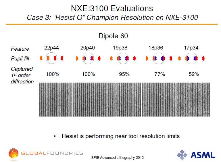
8 EUV NXE:3100 NA=0.25 ArFi NXT:1950i NA=1.35 Dense CH imaging down to 26nm on NXE: nm CHs Single exposure, quasar Positive tone developer 40nm CHs Double dipole exposure Negative tone developer 40nm CHs Single Exposure (Conventional) 26nm CHs Single Exposure (Quasar) 55nm 40nm 26nm CH size and half pitch See presentation Eelco van Setten (ASML) Date / Customer / Slide 8


 range of")

9 Single exposure 14nm node metal 1 features Focus Good printing performance through a focus range of ~100nm for 14nm node 34nm ARM M1 clip (46nm min. pitch) Good printing performance for 14nm node Metal clip (44nm min. pitch) through a focus range of ~120nm Date / Customer / Slide 9


10 NXE:3300B integration status today 7 machines in buildup Development tool Shipment tool Source setup Shipment tool Availability testing Shipment tool Reliability testing Shipment tool Reliability testing Shipment tool Ongoing buildup Shipment tool Ongoing buildup Date / Customer / Slide 10 Shipment tool Ongoing buildup
11 Source Machine is ready for production Source has still way to go Current source performance is ~>10 W vs required for NXE 3300 of W Progress is on the way (REFERENCE TO LAST CYMER AND DPP) But. We can not stop at 250 W. Yan Borodovsky (Intel): EUV source power targets need to be revised upwards ( 1kW average to meet Complementary Lithography and Contacts patterning technology needs (2012 Lithography Workshop, Williamsburg, VA, USA) Date / Customer / Slide 11
12 Why increase in the source requirement The smaller the CD the higher shot noise impact on CDU and LER the higher resist dose is needed Are there ways to improve resist? Possibly: Increase Dill B (from 6->24) Increase mask CD (biasing 1-> 1.2) Increasing aspect ratio of the features (from < 2:1) But we are at the source workshop now. Let us try to rethink what we can do to get to 1000 W source Date / Customer / Slide 12
13 Conventional scaling Date / Customer / Slide 13
14 IF, W Historical perspective on EUV source: Production power requirement, achieved power, productivity Age of choice Age of Xe Age of Sn Age of industrialization ADT NXE-3100 Productivity, wph 0.01 Power desired, W IF Power achieved, W IF Year Averaged and independent on supplier Gap in productivity is being bridged, in reliable power is still 10x to go. Date / Customer / Slide 14 Slide 14
15 Two EUV source concepts Laser-Produced Plasma (LPP) Electrical Discharge (LDP) CO2 drive laser Sn droplets plasma plasma Foil trap Near normal Multilayer collector Sn coated Rotating disc Grazing collector CO 2 laser ignites tin plasma Debris mitigation by background gas and possible magnetic field (Giga) High voltage ignites tin plasma Debris mitigation by foil trap Suppliers: Cymer, Gigaphoton inc. Supplier: XTREME technologies GmbH Presentations David Brandt (Cymer), Gigaphoton Inc., XTREME technologies GmbH Date / Customer / Slide 15

16 LPP now Special thanks to David Brandt Date / Customer / Slide 16


17 LPP scaling LPP shows potential of scaling in low duty cycle experiments Special thanks to David Brandt Date / Customer / Slide 17

18 DPP now Special thanks to Rolf Apetz Date / Customer / Slide 18


19 DPP scaling DPP shows potential of scaling in low duty cycle experiments Special thanks to Rolf Apetz Date / Customer / Slide 19


20 3300 source hardware installing in Veldhoven 3300 vessel Drive laser 3300 vessel installed Source Qualification Tool Date / Customer / Slide 20
21 Conventional scaling of LPP According to Fomenkov et SPIE 2012 : For 185 W EUV 35+ kw laser power is 3% CE thus For 1000 W (@CE= 3%) -> 190+ kw laser power or For 1000 W (@CE= 5%) -> 110+ kw laser power Challenges and question to the conference: CE increase viability at higher powers? SPIE 2012 reported 5%) Laser power scaling or multiplication Maintaining cold gas buffer for lifetime of the mirror at the 3-4x increase of power load Maintaining lifetime of collector at increased (3x-4x) Sn consumption (Is GI collector (Media Lario SPIE 2012) a viable idea in this case? Droplet generator scalability to higher frequencies?. Date / Customer / Slide 21
22 Conventional scaling of DPP (LDP) According to Corthout et EUVL symp 2010: For 107 W EUV 76 kw power input is 2.3% CE thus For 1000 W (@CE= 3%) -> 700+ kw power input is needed Challenges and question to the conference: Is CE increase an option? Will discharge heads still work at this power or jets is a way (Koshelev et al SPIE 2012) How to scale foil trap when > ½ MW is dissipated at a short distance (increase the distance -> collector size and track length). Date / Customer / Slide 22
23 Not conventional scaling Date / Customer / Slide 23
24 Synchrotron wiggler, undulator, FEL Principle: Never made it e- 1. Relativistic electrons traversing a periodic magnetic structure are being bent; 2. Being bent, electrons emit EUV. Prospects before 2000: EUV 1. No debris; 2. Good dose repeatability; 3. High maturity (1999!); 4. High uptime Issues: 1. High CoO; 2. Non-flexible configuration. 3. Not enough power (2005!) 4. Current update: 0.2 W with FLASH (250 m installation) Date / Customer / Slide 24


25 Alternative high power source: free electron laser EUV radiation from an accelerator based source. folded linear accelerator EUV light from amplified undulator radiation average power > 1kW repetition rate > 250 khz Slide 25 Details: Concept Study on an Accelerator based Source for 6.x nm Lithography, Session 11
26 Looking at the FEL again Current update: 0.2 W with FLASH (250 m installation) But theoretically > kw is possible? Date / Customer / Slide 26
27 Summary The EUVL NXE tool is ready to produce great imaging solutions Power of the source has to come still beyond 100+ W and progress is being made as we speak 1000 W is needed for the future Question to the conference: How to do this? Date / Customer / Slide 27
28 Acknowledgements The work presented today, is the result of hard work and dedication of teams at ASML, Cymer, Ushio and many technology partners worldwide Special thanks to David Brandt of Cymer, Rolf Apetz of Xtreme and Diana Tuerke of Zeiss for providing input to this presentation. Date / Customer / Slide 28 Slide 28
EUVL Scanners Operational at Chipmakers. Skip Miller Semicon West 2011
 EUVL Scanners Operational at Chipmakers Skip Miller Semicon West 2011 Outline ASML s Lithography roadmap to support Moore s Law Progress on NXE:3100 (0.25NA) EUV systems Progress on NXE:3300 (0.33NA) EUV
EUV lithography: status, future requirements and challenges
 EUV lithography: status, future requirements and challenges EUVL Dublin Vadim Banine with the help of Rudy Peters, David Brandt, Igor Fomenkov, Maarten van Kampen, Andrei Yakunin, Vladimir Ivanov and many
EUVL getting ready for volume introduction
 EUVL getting ready for volume introduction SEMICON West 2010 Hans Meiling, July 14, 2010 Slide 1 public Outline ASML s Lithography roadmap to support Moore s Law Progress on 0.25NA EUV systems Progress
EUV: Status and Challenges Ahead International Workshop on EUVL, Maui 2010
 EUV: Status and Challenges Ahead International Workshop on EUVL, Maui 2010 Jos Benschop Public Agenda Roadmap Status Challenges Summary & conclusion Slide 2 Public Resolution (half pitch) "Shrink" [nm]
Discovering Electrical & Computer Engineering. Carmen S. Menoni Professor Week 3 armain.
 Discovering Electrical & Computer Engineering Carmen S. Menoni Professor Week 3 http://www.engr.colostate.edu/ece103/semin armain.html TOP TECH 2012 SPECIAL REPORT IEEE SPECTRUM PAGE 28, JANUARY 2012 P.E.
Status and challenges of EUV Lithography
 Status and challenges of EUV Lithography SEMICON Europa Dresden, Germany Jan-Willem van der Horst Product Manager EUV October 10 th, 2013 Slide 2 Contents Introduction NXE:3100 NXE:3300B Summary and acknowledgements
Spring of EUVL: SPIE 2012 AL EUVL Conference Review
 Spring of EUVL: SPIE 2012 AL EUVL Conference Review Vivek Bakshi, EUV Litho, Inc., Austin, Texas Monday, February 20, 2012 The SPIE Advanced Lithography EUVL Conference is usually held close to spring,
Holistic View of Lithography for Double Patterning. Skip Miller ASML
 Holistic View of Lithography for Double Patterning Skip Miller ASML Outline Lithography Requirements ASML Holistic Lithography Solutions Conclusions Slide 2 Shrink Continues Lithography keeps adding value
Reliable High Power EUV Source Technology for HVM: LPP or DPP? Vivek Bakshi, Ph.D. EUV Litho, Inc.
 Reliable High Power EUV Source Technology for HVM: LPP or DPP? Vivek Bakshi, Ph.D. EUV Litho, Inc. Presentation Outline Source Technology Requirements Source Technology Performance DPP LPP Technology Trend
EUV Light Source The Path to HVM Scalability in Practice
 EUV Light Source The Path to HVM Scalability in Practice Harald Verbraak et al. (all people at XTREME) 2011 International Workshop on EUV and Soft X-ray Sources Nov. 2011 Today s Talk o LDP Technology
Bank of America Merrill Lynch Taiwan, Technology and Beyond Conference
 Bank of America Merrill Lynch Taiwan, Technology and Beyond Conference Craig De Young Vice President Investor Relations Taipei, Taiwan March 12, 2013 Forward looking statements Slide 2 Safe Harbor Statement
EUV Supporting Moore s Law
 EUV Supporting Moore s Law Marcel Kemp Director Investor Relations - Europe DB 2014 TMT Conference London September 4, 2014 Forward looking statements This document contains statements relating to certain
Imaging for the next decade
 Imaging for the next decade Martin van den Brink Executive Vice President Products & Technology IMEC Technology Forum 2009 3 June, 2009 Slide 1 Congratulations! ASML and years of making chips better Slide
TWINSCAN XT:1950i Water-based immersion taken to the max Enabling fast, single-exposure lithography at sub 40 nm
 TWINSCAN XT:1950i Water-based immersion taken to the max Enabling fast, single-exposure lithography at sub 40 nm SEMICON West, San Francisco July 14-18, 2008 Slide 1 The immersion pool becomes an ocean
Nikon EUVL Development Progress Update
 Nikon EUVL Development Progress Update Takaharu Miura EUVL Symposium September 29, 2008 EUVL Symposium 2008 @Lake Tahoe T. Miura September 29, 2008 Slide 1 Presentation Outline 1. Nikon EUV roadmap 2.
TSMC Property. EUV Lithography. The March toward HVM. Anthony Yen. 9 September TSMC, Ltd
 EUV Lithography The March toward HVM Anthony Yen 9 September 2016 1 1 st EUV lithography setup and results, 1986 Si Stencil Mask SR W/C Multilayer Coating Optics λ=11 nm, provided by synchrotron radiation
Tin LDP Source Collector Module (SoCoMo) ready for integration into Beta scanner ABSTRACT Keywords : 1. INTRODUCTION
 ready for integration into Beta scanner ABSTRACT Keywords : 1. INTRODUCTION") 1 ) XTREME technologies GmbH, Steinbachstr. 15, 5274 Aachen, Germany 2 ) Gotemba R&D Center, Extreme Ultraviolet Lithography System Development Association (EUVA), 1-9, Komakado, Gotemba, Shizuoka-prefecture,
1 ) XTREME technologies GmbH, Steinbachstr. 15, 5274 Aachen, Germany 2 ) Gotemba R&D Center, Extreme Ultraviolet Lithography System Development Association (EUVA), 1-9, Komakado, Gotemba, Shizuoka-prefecture,
High-NA EUV lithography enabling Moore s law in the next decade
 High-NA EUV lithography enabling Moore s law in the next decade Jan van Schoot, Kars Troost, Alberto Pirati, Rob van Ballegoij, Peter Krabbendam, Judon Stoeldraijer, Erik Loopstra, Jos Benschop, Jo Finders,
2008 European EUVL. EUV activities the EUVL shop future plans. Rob Hartman
 2008 European EUVL EUV activities the EUVL shop future plans Rob Hartman 2007 international EUVL Symposium 28-31 October 2007 2008 international EUVL Symposium 28 Sapporo, September Japan 1 October 2008
EUVL Exposure Tools for HVM: It s Under (and About) Control
 Control") EUVL Exposure Tools for HVM: It s Under (and About) Control Wim van der Zande ASML Director, Research EUV Litho Workshop Amsterdam November 2016 ASML at a EUV Source Workshop Slide 2 The position of EUV
EUVL Exposure Tools for HVM: It s Under (and About) Control Wim van der Zande ASML Director, Research EUV Litho Workshop Amsterdam November 2016 ASML at a EUV Source Workshop Slide 2 The position of EUV
EUV Lithography Transition from Research to Commercialization
 EUV Lithography Transition from Research to Commercialization Charles W. Gwyn and Peter J. Silverman and Intel Corporation Photomask Japan 2003 Pacifico Yokohama, Kanagawa, Japan Gwyn:PMJ:4/17/03:1 EUV
Optics for EUV Lithography
 Optics for EUV Lithography Dr. Sascha Migura, Carl Zeiss SMT GmbH, Oberkochen, Germany 2018 EUVL Workshop June 13 th, 2018 Berkeley, CA, USA The resolution of the optical system determines the minimum
1 st /2nd generation Laser-Produced Plasma source system for HVM EUV lithography
 1 st /2nd generation Laser-Produced Plasma source system for HVM EUV lithography Hakaru Mizoguchi*1, Tamotsu Abe, Yukio Watanabe, Takanobu Ishihara, Takeshi Ohta,Tsukasa Hori, Tatsuya Yanagida, Hitoshi
Newer process technology (since 1999) includes :
 includes :") Newer process technology (since 1999) includes : copper metalization hi-k dielectrics for gate insulators si on insulator strained silicon lo-k dielectrics for interconnects Immersion lithography for masks
Newer process technology (since 1999) includes : copper metalization hi-k dielectrics for gate insulators si on insulator strained silicon lo-k dielectrics for interconnects Immersion lithography for masks
22nm node imaging and beyond: a comparison of EUV and ArFi double patterning
 22nm node imaging and beyond: a comparison of EUV and ArFi double patterning ASML: Eelco van Setten, Orion Mouraille, Friso Wittebrood, Mircea Dusa, Koen van Ingen-Schenau, Jo Finders, Kees Feenstra IMEC:
EUV Source for High Volume Manufacturing: Performance at 250 W and Key Technologies for Power Scaling
 EUV Source for High Volume Manufacturing: Performance at 250 W and Key Technologies for Power Scaling Igor Fomenkov ASML Fellow 2017 Source Workshop, Dublin, Ireland, November 7 th Outline Slide 2 Background
Laser-Produced Sn-plasma for Highvolume Manufacturing EUV Lithography
 Panel discussion Laser-Produced Sn-plasma for Highvolume Manufacturing EUV Lithography Akira Endo * Extreme Ultraviolet Lithography System Development Association Gigaphoton Inc * 2008 EUVL Workshop 11
R&D Status and Key Technical and Implementation Challenges for EUV HVM
 R&D Status and Key Technical and Implementation Challenges for EUV HVM Sam Intel Corporation Agenda Requirements by Process Node EUV Technology Status and Gaps Photoresists Tools Reticles Summary 2 Moore
Japan Update. EUVA (Extreme Ultraviolet Lithography System Development Association) Koichi Toyoda. SOURCE TWG 2 March, 2005 San Jose
 Koichi Toyoda. SOURCE TWG 2 March, 2005 San Jose") 1 Japan Update EUVA (Extreme Ultraviolet Lithography System Development Association) Koichi Toyoda SOURCE TWG 2 March, 2005 San Jose Outline 2 EUVA LPP at Hiratsuka R&D Center GDPP at Gotenba Branch Lab.
1 Japan Update EUVA (Extreme Ultraviolet Lithography System Development Association) Koichi Toyoda SOURCE TWG 2 March, 2005 San Jose Outline 2 EUVA LPP at Hiratsuka R&D Center GDPP at Gotenba Branch Lab.
GIGAPHOTON INTRODUCTION
 GIGAPHOTON INTRODUCTION 15 th September 2017 Tatsuo Enami Director and Senior Executive Officer GIGAPHOTON Copyright Gigaphoton Inc. Outline of Gigaphoton Business Light source business
Mask Technology Development in Extreme-Ultraviolet Lithography
 Mask Technology Development in Extreme-Ultraviolet Lithography Anthony Yen September 6, 2013 Projected End of Optical Lithography 2013 TSMC, Ltd 1976 1979 1982 1985 1988 1991 1994 1997 2000 2003 2007 2012
Laser Produced Plasma Light Source for HVM-EUVL
 Laser Produced Plasma Light Source for HVM-EUVL Akira Endo, Hideo Hoshino, Takashi Suganuma, Krzysztof Nowak, Tatsuya Yanagida, Takayuki Yabu, Takeshi Asayama, Yoshifumi Ueno, Masato Moriya, Masaki Nakano,
The future of EUVL. Outline. by Winfried Kaiser, Udo Dinger, Peter Kuerz, Martin Lowisch, Hans-Juergen Mann, Stefan Muellender,
 The future of EUVL by Winfried Kaiser, Udo Dinger, Peter Kuerz, Martin Lowisch, Hans-Juergen Mann, Stefan Muellender, William H. Arnold, Jos Benshop, Steven G. Hansen, Koen van Ingen-Schenau Outline Introduction
Leadership Through Innovation Litho for the future
 Leadership Through Innovation Litho for the future Deutsche Bank Access Asia Conference 2010 Singapore Craig De Young VP Investor Relations and Corporate Communications May 12, 2010 Public Safe Harbor
DUV. Matthew McLaren Vice President Program Management, DUV. 24 November 2014
 DUV Matthew McLaren Vice President Program Management, DUV 24 Forward looking statements This document contains statements relating to certain projections and business trends that are forward-looking,
Lithography Roadmap. without immersion lithography. Node Half pitch. 248nm. 193nm. 157nm EUVL. 3-year cycle: 2-year cycle: imec 2005
 Lithography Roadmap without immersion lithography Node Half pitch 180 nm 130 nm 90 nm 65 nm 45 nm 32 nm 22 nm 250 nm 180 nm 130 nm 90 nm 65 nm 45 nm 32 nm 248nm 193nm 157nm EUVL 3-year cycle: 2-year cycle:
Development Status of EUV Sources for Use in Alpha-, Beta- and High Volume Chip Manufacturing Tools
 Development Status of EUV Sources for Use in Alpha-, Beta- and High Volume Chip Manufacturing Tools Uwe Stamm, Jürgen Kleinschmidt, Bernd Nikolaus, Guido Schriever, Max Christian Schürmann, Christian Ziener
Advanced Patterning Techniques for 22nm HP and beyond
 Advanced Patterning Techniques for 22nm HP and beyond An Overview IEEE LEOS (Bay Area) Yashesh A. Shroff Intel Corporation Aug 4 th, 2009 Outline The Challenge Advanced (optical) lithography overview Flavors
Light Source Technology Advances to Support Process Stability and Performance Predictability for ArF Immersion Double Patterning
 Light Source Technology Advances to Support Process Stability and Performance Predictability for ArF Immersion Double Patterning Ivan Lalovic, Rajasekhar Rao, Slava Rokitski, John Melchior, Rui Jiang,
PROCEEDINGS OF SPIE. LPP-EUV light source for HVM lithography. T. Saito, Y. Ueno, T. Yabu, A. Kurosawa, S. Nagai, et al.
 PROCEEDINGS OF SPIE SPIEDigitalLibrary.org/conference-proceedings-of-spie LPP-EUV light source for HVM lithography T. Saito, Y. Ueno, T. Yabu, A. Kurosawa, S. Nagai, et al. Invited Paper LPP-EUV light
ASML, Brion and Computational Lithography. Neal Callan 15 October 2008, Veldhoven
 ASML, Brion and Computational Lithography Neal Callan 15 October 2008, Veldhoven Chip makers want shrink to continue (based on the average of multiple customers input) 200 Logic DRAM today NAND Flash Resolution,
Enabling Semiconductor Innovation and Growth
 Enabling Semiconductor Innovation and Growth EUV lithography drives Moore s law well into the next decade BAML 2018 APAC TMT Conference Taipei, Taiwan Craig De Young Vice President IR - Asia IR March 14,
Light Sources for EUV Mask Metrology. Heiko Feldmann, Ulrich Müller
 Light Sources for EUV Mask Metrology Heiko Feldmann, Ulrich Müller Dublin, October 9, 2012 Agenda 1 2 3 4 Actinic Metrology in Mask Making The AIMS EUV Concept Metrology Performance Drivers and their Relation
Scope and Limit of Lithography to the End of Moore s Law
 Scope and Limit of Lithography to the End of Moore s Law Burn J. Lin tsmc, Inc. 1 What dictate the end of Moore s Law Economy Device limits Lithography limits 2 Litho Requirement of Critical Layers Logic
EUV Source Workshop. Organization Committee. Agora 2, World Trade Center Barcelona, Spain, October 19, 2006
 EUV Source Workshop Agora 2, World Trade Center Barcelona, Spain, October 19, 2006 Organization Committee Vivek Bakshi (Chair, SEMATECH), Vadim Banine (ASML), Akira Endo (EUVA), Igor Fomenkov (Cymer),
LPP EUV Source Development and HVM I Productization
 LPP EUV Source Development and HVM I Productization October 19, 2009 David C. Brandt*, Igor V. Fomenkov, Alex I. Ershov, William N. Partlo, David W. Myers Richard L. Sandstrom, Norbert R. Böwering, Alexander
Present Status and Future Prospects of EUV Lithography
 3rd EUV-FEL Workshop Present Status and Future Prospects of EUV Lithography (EUV リソグラフィーの現状と将来展望 ) December 11, 2011 Evolving nano process Infrastructure Development Center, Inc. (EIDEC) Hidemi Ishiuchi
Scaling of Semiconductor Integrated Circuits and EUV Lithography
 Scaling of Semiconductor Integrated Circuits and EUV Lithography ( 半導体集積回路の微細化と EUV リソグラフィー ) December 13, 2016 EIDEC (Emerging nano process Infrastructure Development Center, Inc.) Hidemi Ishiuchi 1 OUTLINE
EUVL Activities in China. Xiangzhao Wang Shanghai Inst. Of Opt. and Fine Mech. Of CAS. (SIOM) Shanghai, China.
 Shanghai, China.") EUVL Activities in China Xiangzhao Wang Shanghai Inst. Of Opt. and Fine Mech. Of CAS. (SIOM) Shanghai, China. wxz26267@siom.ac.cn Projection Optics Imaging System Surface Testing Optical Machining ML Coating
EUVL Activities in China Xiangzhao Wang Shanghai Inst. Of Opt. and Fine Mech. Of CAS. (SIOM) Shanghai, China. wxz26267@siom.ac.cn Projection Optics Imaging System Surface Testing Optical Machining ML Coating
Multiple Patterning for Immersion Extension and EUV Insertion. Chris Bencher Distinguished Member of Technical Staff Applied Materials CTO group
 Multiple Patterning for Immersion Extension and EUV Insertion Chris Bencher Distinguished Member of Technical Staff Applied Materials CTO group Abstract Multiple Patterning for Immersion Extension and
S26 Basic research on 6.x nm EUV generation by laser produced plasma
 S26 Basic research on 6.x nm EUV generation by laser produced plasma Tsukasa Hori, Tatsuya Yanagida, Hitoshi Nagano, Yasunori Wada, Soumagne Georg, Junichi Fujimoto*, Hakaru Mizoguchi* e-mail : tsukasa_hori@komatsu.co.jp
Metrology in the context of holistic Lithography
 Metrology in the context of holistic Lithography Jeroen Ottens Product System Engineer YieldStar, ASML Lithography is at the heart of chip manufacturing Slide 2 25.April.2017 Repeat 30 to 40 times to build
Competitive in Mainstream Products
 Competitive in Mainstream Products Bert Koek VP, Business Unit manager 300mm Fabs Analyst Day 20 September 2005 ASML Competitive in mainstream products Introduction Market share Device layers critical
(Complementary E-Beam Lithography)
") Extending Optical Lithography with C E B L (Complementary E-Beam Lithography) July 13, 2011 4008 Burton Drive, Santa Clara, CA 95054 Outline Complementary Lithography E-Beam Complements Optical Multibeam
Extending Optical Lithography with C E B L (Complementary E-Beam Lithography) July 13, 2011 4008 Burton Drive, Santa Clara, CA 95054 Outline Complementary Lithography E-Beam Complements Optical Multibeam
PUSHING LITHOGRAPHY TO ENABLE ULTIMATE NANO-ELECTRONICS. LUC VAN DEN HOVE President & CEO imec
 PUSHING LITHOGRAPHY TO ENABLE ULTIMATE NANO-ELECTRONICS LUC VAN DEN HOVE President & CEO imec OUTLINE! Industry drivers! Roadmap extension! Lithography options! Innovation through global collaboration
The future of lithography and its impact on design
 The future of lithography and its impact on design Chris Mack www.lithoguru.com 1 Outline History Lessons Moore s Law Dennard Scaling Cost Trends Is Moore s Law Over? Litho scaling? The Design Gap The
Computational Lithography Requirements & Challenges for Mask Making. Naoya Hayashi, Dai Nippon Printing Co., Ltd
 Computational Lithography Requirements & Challenges for Mask Making Naoya Hayashi, Dai Nippon Printing Co., Ltd Contents Introduction Lithography Trends Computational lithography options More Complex OPC
Progress towards Actinic Patterned Mask Inspection. Oleg Khodykin
 Progress towards Actinic Patterned Mask Inspection Oleg Khodykin Outline Status (technical) of EUV Actinic Reticle Inspection program Xe based LPP source as bright and reliable solution Requirements Choice
NXE: 3300B qualified to support customer product development
 ASML s customer magazine 2013 Issue 2 Extending the TWINSCAN NXT platform Computational lithography enables device scaling NXE: 3300B qualified to support customer product development 4 8 10 4 NXE:3300B
Optical Microlithography XXVIII
 PROCEEDINGS OF SPIE Optical Microlithography XXVIII Kafai Lai Andreas Erdmann Editors 24-26 February 2015 San Jose, California, United States Sponsored by SPIE Cosponsored by Cymer, an ASML company (United
EUV Resist Materials and Process for 16 nm Half Pitch and Beyond
 EUV Workshop 2013 June 13, 2013 EUV Resist Materials and Process for 16 nm Half Pitch and Beyond Yoshi Hishiro JSR Micro Inc. No13-2400-056 Challenge for EUV Resist & JSR approaches EUV Resist Resolution,
Facing Moore s Law with Model-Driven R&D
 Facing Moore s Law with Model-Driven R&D Markus Matthes Executive Vice President Development and Engineering, ASML Eindhoven, June 11 th, 2015 Slide 2 Contents Introducing ASML Lithography, the driving
Towards an affordable Cost of Ownership for EUVL. Melissa Shell Principal Engineer & Program Manager, EUVL Research Components Research October 2006
 Towards an affordable Cost of Ownership for EUVL Melissa Shell Principal Engineer & Program Manager, EUVL Research Components Research October 2006 1 Robert Bristol Heidi Cao Manish Chandhok Michael Leeson
Benefit of ArF immersion lithography in 55 nm logic device manufacturing
 Benefit of ArF immersion lithography in 55 nm logic device manufacturing Takayuki Uchiyama* a, Takao Tamura a, Kazuyuki Yoshimochi a, Paul Graupner b, Hans Bakker c, Eelco van Setten c, Kenji Morisaki
Optical Lithography. Keeho Kim Nano Team / R&D DongbuAnam Semi
 Optical Lithography Keeho Kim Nano Team / R&D DongbuAnam Semi Contents Lithography = Photolithography = Optical Lithography CD : Critical Dimension Resist Pattern after Development Exposure Contents Optical
Closed Loop Registration Control (RegC ) Using PROVE as the Data Source for the RegC Process
 Using PROVE as the Data Source for the RegC Process") Invited Paper Closed Loop Registration Control (RegC ) Using PROVE as the Data Source for the RegC Process Erez Graitzer 1 ; Avi Cohen 1 ; Vladimir Dmitriev 1 ; Itamar Balla 1 ; Dan Avizemer 1 Dirk Beyer
Invited Paper Closed Loop Registration Control (RegC ) Using PROVE as the Data Source for the RegC Process Erez Graitzer 1 ; Avi Cohen 1 ; Vladimir Dmitriev 1 ; Itamar Balla 1 ; Dan Avizemer 1 Dirk Beyer
Imec pushes the limits of EUV lithography single exposure for future logic and memory
 Edition March 2018 Semiconductor technology & processing Imec pushes the limits of EUV lithography single exposure for future logic and memory Imec has made considerable progress towards enabling extreme
Short wavelength light source for semiconductor manufacturing: Challenge from excimer laser to LPP-EUV light source
 Introduction of Products Short wavelength light source for semiconductor manufacturing: Challenge from excimer laser to LPP-EUV light source Hakaru Mizoguchi Takashi Saito Noritoshi Itou Taku Yamazaki
Shooting for the 22nm Lithography Goal with the. Coat/Develop Track. SOKUDO Lithography Breakfast Forum 2010 July 14 (L1)
") Shooting for the 22nm Lithography Goal with the Coat/Develop Track SOKUDO Lithography Breakfast Forum 2010 July 14 (L1) Three (3) different exposure options for 22nm: Public External (L1) MAPPER Lithography
Shooting for the 22nm Lithography Goal with the Coat/Develop Track SOKUDO Lithography Breakfast Forum 2010 July 14 (L1) Three (3) different exposure options for 22nm: Public External (L1) MAPPER Lithography
EUVL Activities in China
 2014 EUVL Workshop EUVL Activities in China Yanqiu Li, Zhen Cao Beijing Institute of Technology (BIT) Email: liyanqiu@bit.edu.cn Activities only refer to published papers June 25, 2014 OUTLINE Overview
EUVL: Challenges to Manufacturing Insertion
 Journal of Photopolymer Science and Technology Volume 30, Number 5 (2017) 599-604 C 2017SPST Technical Paper EUVL: Challenges to Manufacturing Insertion Obert R. Wood II * Strategic Lithography Technology,
EUVL Activities in China
 EUVL Activities in China Yanqiu Li Beijing Institute of Technology (BIT) Phone/Fax: 010-68918443 Email: liyanqiu@bit.edu.cn June 13, 2013 HI Contents Overview of EUVL in China System EUVL Optics EUV Metrology
IMEC update. A.M. Goethals. IMEC, Leuven, Belgium
 IMEC update A.M. Goethals IMEC, Leuven, Belgium Outline IMEC litho program overview ASML ADT status 1 st imaging Tool description Resist projects Screening using interference litho K LUP / Novel resist
A Closer Look at ASML. September 26-27, 2002
 A Coser Look at ASML September 26-27, 2002 TWINSCAN Outine Introduction TWINSCAN roadmap Dua stage technoogy Productivity TWINSCAN dua stage performance Concusion Outine Introduction TWINSCAN roadmap Dua
EUVL: Challenges to Manufacturing Insertion
 EUVL: Challenges to Manufacturing Insertion Obert R Wood II International Workshop on EUV Lithography CXRO, LBNL, Berkeley, California 14 June 2017 EUV Critical Issues List EUV Critical Issues, as identified
450mm and Moore s Law Advanced Packaging Challenges and the Impact of 3D
 450mm and Moore s Law Advanced Packaging Challenges and the Impact of 3D Doug Anberg VP, Technical Marketing Ultratech SOKUDO Lithography Breakfast Forum July 10, 2013 Agenda Next Generation Technology
Advanced Digital Integrated Circuits. Lecture 2: Scaling Trends. Announcements. No office hour next Monday. Extra office hour Tuesday 2-3pm
 EE241 - Spring 20 Advanced Digital Integrated Circuits Lecture 2: Scaling Trends and Features of Modern Technologies Announcements No office hour next Monday Extra office hour Tuesday 2-3pm 2 1 Outline
2009 International Workshop on EUV Lithography
 Contents Introduction Absorber Stack Optimization Non-flatness Correction Blank Defect and Its Mitigation Wafer Printing Inspection Actinic Metrology Cleaning and Repair Status Remaining Issues in EUV
Multilayer Collector Optics for Water Window Microscopy
 Multilayer Collector Optics for Water Window Microscopy 2015 International Workshop on EUV and soft X-Ray Sources Torsten Feigl 1, Hagen Pauer 1, Tobias Fiedler 1, Marco Perske 1, Holger Stiel 2,3, Christian
Fiber Lasers for EUV Lithography
 Fiber Lasers for EUV Lithography A. Galvanauskas, Kai Chung Hou*, Cheng Zhu CUOS, EECS Department, University of Michigan P. Amaya Arbor Photonics, Inc. * Currently with Cymer, Inc 2009 International Workshop
Light Sources for High Volume Metrology and Inspection Applications
 Light Sources for High Volume Metrology and Inspection Applications Reza Abhari International Workshop on EUV and Soft X- Ray Sources November 9-11, 2015, Dublin, Ireland Reza S. Abhari 11/10/15 1 Inspection
Optical Maskless Lithography (OML) Project Status
 Project Status") Optical Maskless Lithography (OML) Project Status Timothy O Neil, Arno Bleeker, Kars Troost SEMATECH ML 2 Conference January 2005 / Slide 1 Agenda Introduction and Principles of Operation DARPA Program
Optical Maskless Lithography (OML) Project Status Timothy O Neil, Arno Bleeker, Kars Troost SEMATECH ML 2 Conference January 2005 / Slide 1 Agenda Introduction and Principles of Operation DARPA Program
Update on 193nm immersion exposure tool
 Update on 193nm immersion exposure tool S. Owa, H. Nagasaka, Y. Ishii Nikon Corporation O. Hirakawa and T. Yamamoto Tokyo Electron Kyushu Ltd. January 28, 2004 Litho Forum 1 What is immersion lithography?
LPP collector mirrors coating, metrology and refurbishment
 LPP collector mirrors coating, metrology and refurbishment 2013 International Workshop on EUV and soft X-Ray Sources Torsten Feigl, Marco Perske, Hagen Pauer, Tobias Fiedler optix fab GmbH Christian Laubis,
Progress in full field EUV lithography program at IMEC
 Progress in full field EUV lithography program at IMEC A.M. Goethals*, G.F. Lorusso*, R. Jonckheere*, B. Baudemprez*, J. Hermans*, F. Iwamoto 1, B.S. Kim 2, I.S. Kim 2, A. Myers 3, A. Niroomand 4, N. Stepanenko
2014 International Workshop on EUV Lithography
 2014 International Workshop on EUV Lithography Vivek Bakshi Workshop Summary June 23-27, 2014 Makena Beach & Golf Resort, Maui, Hawaii (Workshop Summary are notes taken by author during the workshop. Please
Challenges of EUV masks and preliminary evaluation
 Challenges of EUV masks and preliminary evaluation Naoya Hayashi Electronic Device Laboratory Dai Nippon Printing Co.,Ltd. EUV Mask Workshop 2004 1 Contents Recent Lithography Options on Roadmap Challenges
Akira Miyake, Chidane Ouchi, International EUVL Symposium, October , Kobe Slide 1
 Development Status of Canon s EUVL Exposure Tool Akira Miyake, Chidane Ouchi, Hideki Morishima, and Hiroyoshi Kubo Canon Inc. International EUVL Symposium, October 18 2010, Kobe Slide 1 Outline EUVL Exposure
1 st generation Laser-Produced Plasma source system for HVM EUV lithography
 1 st generation Laser-Produced Plasma source system for HVM EUV lithography Hakaru Mizoguchi *1, Tamotsu Abe, Yukio Watanabe, Takanobu Ishihara, Takeshi Ohta, Tsukasa Hori, Akihiko Kurosu, Hiroshi Komori,
Beyond Immersion Patterning Enablers for the Next Decade
 Beyond Immersion Patterning Enablers for the Next Decade Colin Brodsky Manager and Senior Technical Staff Member Patterning Process Development IBM Semiconductor Research & Development Center Hopewell
CO 2 / Sn LPP EUV Sources for device development and HVM
 CO 2 / Sn LPP EUV Sources for device development and HVM David C. Brandt, Igor V. Fomenkov, Nigel R. Farrar, Bruno La Fontaine, David W. Myers, Daniel J. Brown, Alex I. Ershov, Richard L. Sandstrom, Georgiy
Power scaling of picosecond thin disc laser for LPP and FEL EUV sources
 Power scaling of picosecond thin disc laser for LPP and FEL EUV sources A. Endo 1,2, M. Smrz 1, O. Novak 1, T. Mocek 1, K.Sakaue 2 and M.Washio 2 1) HiLASE Centre, Institute of Physics AS CR, Dolní Břežany,
Public. Introduction to ASML. Ron Kool. SVP Corporate Strategy and Marketing. March-2015 Veldhoven
 Public Introduction to ASML Ron Kool SVP Corporate Strategy and Marketing March-2015 Veldhoven 1991 1992 1993 1994 1995 1996 1997 1998 1999 2000 2001 2002 2003 2004 2005 2006 2007 2008 2009 2010 2011 2012
Novel EUV Resist Development for Sub-14nm Half Pitch
 EUV Workshop 2015 Maui, HI P64 Novel EUV Resist Development for Sub-14nm Half Pitch Yoshi Hishiro JSR Micro Inc. EUV Workshop, June 17, 2015 1 Contents Requirement for sub-14nm HP EUV resist JSR strategy
Jung Sik Kim, Seongchul Hong, Jae Uk Lee, Seung Min Lee, and Jinho Ahn*
 Jung Sik Kim, Seongchul Hong, Jae Uk Lee, Seung Min Lee, and Jinho Ahn* Photon shot noise effect in EUVL Degrades stochastic imaging performance Suggestion of a thin attenuated PSM Comparing PSM with conventional
Actinic Review of EUV Masks: Performance Data and Status of the AIMS TM EUV System
 Actinic Review of EUV Masks: Performance Data and Status of the AIMS TM EUV System Dirk Hellweg*, Markus Koch, Sascha Perlitz, Martin Dietzel, Renzo Capelli Carl Zeiss SMT GmbH, Rudolf-Eber-Str. 2, 73447
Technological Challenges in Semiconductor Lithography
 Technological Challenges in Semiconductor Lithography some aspects of projection lithography technology and its position in high tech industry and academia Ramin Badie ASML Research 2014 What do I want
Bridging the Gap Between Tools & Applications
 EUV Workshop, Dublin 7-9 November 2011 The EUV Laser Program at the University of Bern Bridging the Gap Between Tools & Applications D. Bleiner, J.E. Balmer, F. Staub, J. Fei, L. Masoudnia, M. Ruiz Universität
Impact of 3-D Mask Effects on CD and Overlay over Image Field in Extreme Ultraviolet Lithography
 Impact of 3-D Mask Effects on CD and Overlay over Image Field in Extreme Ultraviolet Lithography 5 th International EUV Symposium Barcelona, Spain Sven Trogisch Markus Bender Frank-Michael Kamm Disclaimer
5 th Annual ebeam Initiative Luncheon SPIE February 26, Aki Fujimura CEO D2S, Inc. Managing Company Sponsor ebeam Initiative
 5 th Annual ebeam Initiative Luncheon SPIE February 26, 2013 Aki Fujimura CEO D2S, Inc. Managing Company Sponsor ebeam Initiative ebeam Writes All Chips The ebeam Initiative: Is an educational platform