Enabling Semiconductor Innovation and Growth
|
|
|
- Damon Dean
- 6 years ago
- Views:
Transcription


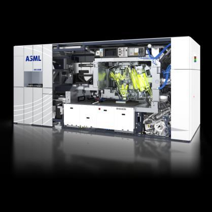
1 Enabling Semiconductor Innovation and Growth EUV lithography drives Moore s law well into the next decade BAML 2018 APAC TMT Conference Taipei, Taiwan Craig De Young Vice President IR - Asia IR March 14, 2018
2 Forward looking statements This document contains statements relating to certain projections, business trends and other matters that are forward-looking, including statements with respect to expected trends and outlook, including expected trends in the semiconductor market, expected annual operating profit, systems backlog, statements with respect to expected revenue growth in the semiconductor market, including expected forecast growth by market, the expected relative semiconductor content in automotive innovations by 2030, expected growth drivers in lithography demand in 2020, statements with respect to industry shrink roadmaps, EUV insertion plans and customer roadmaps, statements with respect to the expected continuation of scaling and transistor density by 2030, expectations with respect to EUV, including expected benefits, including lithography cost reduction and the expected benefits of High NA, target performance, EUV industrialization, including availability and throughput, shipments and the expectation that the installed base of EUV systems will double in 2018, the expected innovation pipeline in the next 10 years and beyond, the expected increased impact of new scalable memory types in the next 10 years and the expectation that such types will continue driving lithography, statements with respect to shrink being a key driver supporting innovation and providing long-term industry growth, lithography enabling affordable shrink and delivering value to customers, and statements with respect to the expected continuation of Moore's law and that EUV and scaling and shrinking will continue to support and enable Moore s law and drive long term value for ASML beyond the next decade. You can generally identify these statements by the use of words like "may", "will", "could", "should", "project", "believe", "anticipate", "expect", "plan", "estimate", "forecast", "potential", "intend", "continue", "targets", "commits to secure" and variations of these words or comparable words. These statements are not historical facts, but rather are based on current expectations, estimates, assumptions and projections about the business and our future financial results and readers should not place undue reliance on them. Forward-looking statements do not guarantee future performance and involve risks and uncertainties. These risks and uncertainties include, without limitation, economic conditions, product demand and semiconductor equipment industry capacity, worldwide demand and manufacturing capacity utilization for semiconductors, including the impact of general economic conditions on consumer confidence and demand for our customers' products, competitive products and pricing, the impact of any manufacturing efficiencies and capacity constraints, performance of our systems, the continuing success of technology advances and the related pace of new product development and customer acceptance of new products including EUV, the number and timing of EUV systems expected to be shipped and recognized in revenue, delays in EUV systems production and development and volume production by customers, including meeting development requirements for volume production, demand for EUV systems being sufficient to result in utilization of EUV facilities in which ASML has made significant investments, our ability to enforce patents and protect intellectual property rights, the outcome of intellectual property litigation, availability of raw materials, critical manufacturing equipment and qualified employees, trade environment, changes in exchange rates, changes in tax rates, available cash and liquidity, our ability to refinance our indebtedness, distributable reserves for dividend payments and share repurchases, results of the new share repurchase plan and other risks indicated in the risk factors included in ASML's Annual Report on Form 20-F and other filings with the US Securities and Exchange Commission. These forward-looking statements are made only as of the date of this document. We do not undertake to update or revise the forward-looking statements, whether as a result of new information, future events or otherwise. Slide 2 January 17, 2018


3 Semiconductor Scaling has changed how we Transistor density Slide 3 LIVE WORK PLAY Millions per mm 2


4 Insatiable need to transfer, store and analyse data drives a continuous and growing demand for semiconductors Slide 4 Consumer Electronics Smartphones PC, laptop, tablets Factory Automation Autonomous driving


5 Scaling/Shrinking Supports Moore s Law Moore s Law is underpinning a business model Slide 5 1 IC performance improvement at similar cost Takeaways Part of the profits are reinvested in R&D, equipment 4 2 Improved electronic devices and new applications >$250+ billion of annual operating profit is riding on the industry s ability to keep this cycle going >$250+ billion of operating profit per year Consumers and businesses upgrade or adopt new products 3
6 ebay Cognizant ADP NetEase Yahoo Murata TE Connect Canon ASML operates in a highly profitable value chain with strong incentives to compete and drive innovation Slide 6 ASML Applied Materials LAM Research KLA-Tencor TEL Semi Equipment Semi Manufacturing ASML Peers Semi Non-Semi Semi Design There remains a lot of income generated Total EBIT, B$ Baidu NVIDIA Hardware ~250 ~275 ~290 ~280 / Alphabet Software & Services Top technology companies in our ecosystem (EBIT CY2016, B$) Source: Bloomberg (GICS 45 classification)
7 WW semiconductor Revenue [B$] Leading edge Logic and Memory processes drive growth in semiconductor markets Slide 7 Revenue growth is coming from those segments where roadmap innovation continues: advanced logic, DRAM and NAND (nonvolatile memory) Lately we ve seen the following trends in semiconductor markets: WW Semiconductor revenue [B$] CAGR 5% 2D NAND Logic > 20 nm Legacy DRAM Logic 20 nm 3D NAND CAGR 14% CAGR -2% Strong transition to 3D-NAND to continue enabling large capacities at lower cost Slowing DRAM roadmap leading to lower bit growth resulting in price increases, triggering capacity investments Increasing focus on new memory devices (i.e. x-point) Continuing strong drive for logic shrink with process improvements coming on an annual cadence Source: ASML analysis, Gartner
![Semiconductors drive 80% of automotive innovations Expected to represent 50% of the cost of goods in 2030 (per Audi) Slide 8 Relative Semiconductor content in automotive [%COG]](/docs-images/79/80302073/images/8-0.jpg "100 90 80 70 60 50 40 30 20 10 0 1991 2015 2020 2030 Source: Berthold Hellenhtal, Audi, Cross industry collaboration networks accelerate innovations, ISS Europe, Munich, March")
8 Semiconductors drive 80% of automotive innovations Expected to represent 50% of the cost of goods in 2030 (per Audi) Slide 8 Relative Semiconductor content in automotive [%COG] Source: Berthold Hellenhtal, Audi, Cross industry collaboration networks accelerate innovations, ISS Europe, Munich, March 2017

 Data volume &")


9 NAND CHINA IoT Disruptive trends also drive litho demand Growth drivers: 2017 to Slide 9 Storage Class Memory Growth and transition to 3D NAND China Greenfield Investments Emerging connected devices market (IoT) Data volume & complexity Sensors & Devices You are here Images & Media Text Internet of Things will connect a growing number of devices from 12 billion in 2012 to 50 billion in 2020 IoT devices shipments, B units Source: John Kelly III, IBM, December 2015 Enterprise Chinese government supports massive investment into domestic semi industry 0 +65% p.a
 Multi-patterning (+ source-mask optimization, control loops) Immersion (+ optical proximity")
10 Transistor density Scaling will continue towards 1 billion transistors per mm 2 We are ready to support the Semi industry s ambition through the extension of Moore s Law Slide 10 Millions per mm 2 High-NA EUV EUV (+ pattern fidelity control) Multi-patterning (+ source-mask optimization, control loops) Immersion (+ optical proximity correction)

11 EUV A New Technology in Lithography Slide 11 New technology transitions: customer perspective EUV progress & plans EUV infrastructure EUV extendibility ~4 m ~3 m ~8 m
12 What is EUV? A litho technology that delivers 3x -> 5x Resolution Enhancement Slide 12 Resolution = k 1 x l ArF immersion EUV NA k 1 difficulty, limit = 0.25 k 1 = strong OPC mask k 1 = 0.32 OPC mask l Wavelength 193nm 13.5nm NA Numerical Aperture NA 1.35 Maximum NA 0.33 Current NA > 0.5 Future Resolution Minimum pitch 76nm 38nm half pitch 26nm 13nm half pitch < 16nm < 8nm half pitch
13 Dilemmas when adopting a game-changing technology Early decision making Slide 13 It works It does not work We have it We do not have it??
14 How customers approach new technology insertions Slide 14 Visionary/champion R&D enthusiasm First results Business manager Shouldn t we go for this? Manufacturing push back Tough criteria, entrance hurdles Dynamics: progress vs. milestones Product roadmap timing Business decision with up/down ticks Different risk appetite per customer and per segment EUV Case Done To be addressed To be considered
15 Technology transitions: decisions based on early results You have to move to where the puck will be, not where it is (Wayne Gretzky) Slide 15 Decision point Desired performance at the time of volume ramp Performance Increasing complexity introduces additional risk - lengthening leadtimes Time


16 General rule of New Technology adoption Slide 16 Early adoption is risky Late adoption is expensive

17 EUV rewards at 7nm are clear: simpler process, shorter cycle time enabling faster yield ramp and time to market 90 Typical # Litho Passes Modelled 7nm Cycle Time, weeks Slide 17 Jan % -21% ArFi only 75-19% 70 EUV Low 65-33% /16nm 10nm 7nm EUV High Dr. Gary Patton, Global Foundries SEMI ISS 2017


18 EUV introduction delivers compelling benefits in layout flexibility and process simplification Slide 18 Jan D EUV patterning More layout flexibility for designers Simpler process integration for engineers EUV process simplification Superior device performance Improved device variability Esin Terzioglu, Qualcomm, International Symposium on EUV, October, 2014 Jeffrey Shearer et al, IBM, AVS, November 2014 Resulting in more effective shrink + higher yields


19 # Process steps for 1 patterning step EUV alternatives are very costly and complex Immersion Multiple Patterning EUV Slide 19 Process Steps CMP Dry Etch Metrology Lithography Track Deposition Clean Hard mask LE3 = 3x Litho-Etch, Triple patterning LE4 = 4x Litho-Etch, Quad patterning SAQP = Spacer Assisted Quad Patterning Cut = Separate Litho-Etch step 0 LE3 LE4 SAQP + 3 cuts Single exposure


20 Relative Cost per Pixel EUV enables continued Litho cost reduction PAS 2500/10 PAS 5500/60 Slide 20 Res. 900nm, 150mm 66wph 1 Res. 450nm 200mm 48wph XT: Resolution 65nm 300mm 145wph NXE:3400 AT: Res. 110nm 300mm 102wph NXT:1950i Res. 13nm 300mm 125wph Res 38nm, 300mm 190wph TBD
21 Slide 21 So where are we now?


22 EUV industrialisation: from technology demonstration to HVM System Slide 22 Resolution : Overlay : Throughput : 40 nm 15 nm 0.05 WPH 3x 10x 2,500x 13 nm 1.5 nm 125 WPH


23 Significant progress in EUV industrialisation Slide 23 EUV Source & Throughput Proven Power 1 & Wafers/Hour 2 EUV Availability Uptime % Cumulative EUV wafer exposures NXE:3xxx, Wafers Source Power Throughput, W/Hr 250W 3 300W 100% >2M 125 W/Hr 155W/Hr 0.6M 1.1M Uptime Planned upgrades 0.3M Target 0% Demonstrated on test rig, 2 Demonstrated at ASML or Customer, 3 Enables 145W/Hr on NXE:3400B


24 Evolution of EUV Infrastructure readiness Slide 24 EUV Infrastructure 11/14 10/15 11/15 10/16 02/17 E-beam mask inspection AIMS Mask Inspection Actinic Blank Inspection From 2016 EUVL Symposium EUV Pellicle EUV Blank Quality Blank multi-layer deposition tool EUV Resist QC Actinic Patterned Mask Inspection Source: Britt Turkot, Intel, International Workshop on EUV Lithography, California, June 2017.
25 Storage Memory Storage Class Memory Performance Memory Logic Industry shrink roadmap and EUV insertion plans EUV in Production Slide 25 HVM nm nm 10 nm 7 nm 5 nm 3 nm Node name DRAM X 1Y 1Z next Minimum half pitch PC-RAM, ReRAM etc. 2X /x2 1X /x4 1Y /x8 1Z /x8 Minimum half pitch /x number of layers Planar Floating Gate NAND Today s status Production D NAND Development 1 Research 1 Roadmap 2 x24 x32 x48 x64 >x96 >x128 >x192 >x200 x number of layers Source: 1) Customers - public statements,, IC Knowledge LLC; 2) ASML extrapolations
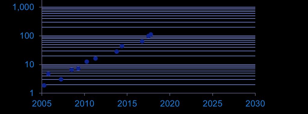
26 ...which is supported by Customer shipments and orders Installed Base of EUV systems expected to double in 2018 Slide 26 NXE:33x0 and NXE:3400 Shipments and Installed Base R&D HVM ramp Installed Base Planned Shipments End Q4 17 order backlog: 28 systems from 6 Customers

27 And by recent customer statements on EUV insertion Slide 27
28 Slide 28 What s next?
29 Customer roadmaps extend 10 years 1000 Slide 29 1 nm 2 nm Transitor Density MTr / mm /40 nm 28 nm 28/32 nm 20 nm 14/16 nm 10 nm 7 nm 5 nm 3 nm Density extrapolated, timing based on customer reviews HVM Wafer Start Date

30 Resolution, nm = k 1 x Wavelength / NA High NA extends EUV with a larger resolution step than immersion did for ArF 1, XT: % NXE:3400 EUV 13.5 nm 13nm, 0.33 NA >10x 436, g-line 365, i-line 248, KrF 193, ArF Slide 31 Wavelength, nm 10 1 g-line i-line ArF Immersion KrF EUV Development systems xx% ArF 193nm 65nm, 0.93 NA Increase in NA NXT:1950i ArFi 193nm 38nm, 1.35 NA % 13.5, EUV Timing TBD High NA EUV EUV, 13.5nm <8nm, >0.5 NA
31 Relative Cost per Pixel High NA EUV extends cost per pixel reduction PAS 2500/10 PAS 5500/60 Slide Res. 900nm, 150mm 66wph Res. 450nm 200mm 48wph XT: Resolution 65nm 300mm 145wph NXE:3400 AT:850 High NA EUV Res. 110nm 300mm 102wph NXT:1950i Res. 13nm 300mm 125wph Res. <8nm 300mm 185wph Res 38nm, 300mm 190wph TBD 2023


32 EUV shrink + Holistic Litho (addressing k 1 ) keeps Moore s Law affordable Slide 32 Exposure with high order optimisation Computational Lithography Ensure measurement captures a maximum of relevant information Optical & e-beam Metrology

33 Our innovation pipeline will enable advanced imaging and imaging process control the next 10 years and beyond Slide 33


34 EUV Summary Slide 34 7nm Customers are targeting EUV introduction at 7nm to take advantage of process complexity, cycle time, IC shrink, yield, & performance benefits Key EUV industrialisation & performance milestones have been achieved in 2017, together with solid progress in EUV mask and resist infrastructure EUV introduction enables a return to Litho enabled cost reduction with the opportunity to extend multiple generations ASML is investing in a roadmap to enable continued Holistic Lithography scaling for the coming decade

35 What this means for ASML As IC units grow and Litho Intensity grows.. ASML grows! Slide 35
36 Summary - Our customers and their environment Strong incentives for the entire industry to continue IC performance and cost improvements, now also driving system innovations Our logic customers have roadmaps that extend to 2027 and are not planning to slow down scaling Memory market is growing and performance improvements continue, enabled by 3D stacking and new scalable memory types. The latter will have an increasing impact the coming 10 years and continue to drive lithography Slide 36

37
DUV. Matthew McLaren Vice President Program Management, DUV. 24 November 2014
 DUV Matthew McLaren Vice President Program Management, DUV 24 Forward looking statements This document contains statements relating to certain projections and business trends that are forward-looking,
EUV Supporting Moore s Law
 EUV Supporting Moore s Law Marcel Kemp Director Investor Relations - Europe DB 2014 TMT Conference London September 4, 2014 Forward looking statements This document contains statements relating to certain
Bank of America Merrill Lynch Taiwan, Technology and Beyond Conference
 Bank of America Merrill Lynch Taiwan, Technology and Beyond Conference Craig De Young Vice President Investor Relations Taipei, Taiwan March 12, 2013 Forward looking statements Slide 2 Safe Harbor Statement
CLSA Investors Forum 2017
 CLSA Investors Forum 2017 Grand Hyatt Hong Kong Craig De Young Vice President Investor Relations September 11-15 2017 Forward looking statements Slide 2 This document contains statements relating to certain
TWINSCAN XT:1950i Water-based immersion taken to the max Enabling fast, single-exposure lithography at sub 40 nm
 TWINSCAN XT:1950i Water-based immersion taken to the max Enabling fast, single-exposure lithography at sub 40 nm SEMICON West, San Francisco July 14-18, 2008 Slide 1 The immersion pool becomes an ocean
EUVL getting ready for volume introduction
 EUVL getting ready for volume introduction SEMICON West 2010 Hans Meiling, July 14, 2010 Slide 1 public Outline ASML s Lithography roadmap to support Moore s Law Progress on 0.25NA EUV systems Progress
Competitive in Mainstream Products
 Competitive in Mainstream Products Bert Koek VP, Business Unit manager 300mm Fabs Analyst Day 20 September 2005 ASML Competitive in mainstream products Introduction Market share Device layers critical
Doug Dunn ASML President and Chief Executive Officer Deutsche Bank Conference London, England September 19, / Slide 1
 Doug Dunn ASML President and Chief Executive Officer Deutsche Bank Conference London, England September 19, 2003 / Slide 1 Safe Harbor Safe Harbor Statement under the U.S. Private Securities Litigation
Holistic View of Lithography for Double Patterning. Skip Miller ASML
 Holistic View of Lithography for Double Patterning Skip Miller ASML Outline Lithography Requirements ASML Holistic Lithography Solutions Conclusions Slide 2 Shrink Continues Lithography keeps adding value
Lithography Industry Collaborations
 Accelerating the next technology revolution Lithography Industry Collaborations SOKUDO Breakfast July 13, 2011 Stefan Wurm SEMATECH Copyright 2009 SEMATECH, Inc. SEMATECH, and the SEMATECH logo are registered
Public. Introduction to ASML. Ron Kool. SVP Corporate Strategy and Marketing. March-2015 Veldhoven
 Public Introduction to ASML Ron Kool SVP Corporate Strategy and Marketing March-2015 Veldhoven 1991 1992 1993 1994 1995 1996 1997 1998 1999 2000 2001 2002 2003 2004 2005 2006 2007 2008 2009 2010 2011 2012
Leadership Through Innovation Litho for the future
 Leadership Through Innovation Litho for the future Deutsche Bank Access Asia Conference 2010 Singapore Craig De Young VP Investor Relations and Corporate Communications May 12, 2010 Public Safe Harbor
Imaging for the next decade
 Imaging for the next decade Martin van den Brink Executive Vice President Products & Technology IMEC Technology Forum 2009 3 June, 2009 Slide 1 Congratulations! ASML and years of making chips better Slide
EUVL Scanners Operational at Chipmakers. Skip Miller Semicon West 2011
 EUVL Scanners Operational at Chipmakers Skip Miller Semicon West 2011 Outline ASML s Lithography roadmap to support Moore s Law Progress on NXE:3100 (0.25NA) EUV systems Progress on NXE:3300 (0.33NA) EUV
EUV lithography: today and tomorrow
 EUV lithography: today and tomorrow Vadim Banine, Stuart Young, Roel Moors Dublin, October 2012 Resolution/half pitch, "Shrink" [nm] EUV DPT ArFi ArF KrF Industry roadmap towards < 10 nm resolution Lithography
Nikon Medium Term Management Plan
 NIKON CORPORATION Mar.30,2006 Nikon Medium Term Management Plan March 30, 2006 NIKON CORPORATION This presentation contains forward-looking statements with respect to future results, performance and achievements
21 st Annual Needham Growth Conference
 21 st Annual Needham Growth Conference Investor Presentation January 15, 2019 Safe Harbor Statement The information contained in and discussed during this presentation may include forward-looking statements
Intel Technology Journal
 Volume 06 Issue 02 Published, May 16, 2002 ISSN 1535766X Intel Technology Journal Semiconductor Technology and Manufacturing The Intel Lithography Roadmap A compiled version of all papers from this issue
(Complementary E-Beam Lithography)
") Extending Optical Lithography with C E B L (Complementary E-Beam Lithography) July 13, 2011 4008 Burton Drive, Santa Clara, CA 95054 Outline Complementary Lithography E-Beam Complements Optical Multibeam
Extending Optical Lithography with C E B L (Complementary E-Beam Lithography) July 13, 2011 4008 Burton Drive, Santa Clara, CA 95054 Outline Complementary Lithography E-Beam Complements Optical Multibeam
Multiple Patterning for Immersion Extension and EUV Insertion. Chris Bencher Distinguished Member of Technical Staff Applied Materials CTO group
 Multiple Patterning for Immersion Extension and EUV Insertion Chris Bencher Distinguished Member of Technical Staff Applied Materials CTO group Abstract Multiple Patterning for Immersion Extension and
Credit Suisse European Technology Conference 2008
 Credit Suisse European Technoogy Conference 2008 ASML continues to execute its eadership strategy and expects gradua order pick-up Franki D Hoore Director European Investor Reations London, 15 May 2008
ASML Market dynamics. Dave Chavoustie EVP Sales Analyst Day, September 30, 2004
 ASML Market dynamics Dave Chavoustie EVP Sales Analyst Day, September 30, 2004 Agenda! Market Overview! Growth Opportunities! 300mm Market! Asia Overview / Slide 2 ASML Unit Market Share Trend 60% 12 &
Holistic Lithography. Christophe Fouquet. Executive Vice President, Applications. 24 November 2014
 Holistic Lithography Christophe Fouquet Executive Vice President, Applications 24 Holistic Lithography Introduction Customer Problem: Beyond 20nm node scanner and non scanner contributions must be addressed
Lithography. International SEMATECH: A Focus on the Photomask Industry
 Lithography S P E C I A L International SEMATECH: A Focus on the Photomask Industry by Wally Carpenter, International SEMATECH, Inc. (*IBM Corporation Assignee) It is well known that the semiconductor
Limitations and Challenges to Meet Moore's Law
 Limitations and Challenges to Meet Moore's Law Sept 10, 2015 Sung Kim sung_kim@amat.com State of the art: cleanroom toolsets metrology analysis module development test & reliability Introduction Why do
Global Artificial Intelligence (AI) Semiconductor Market: Size, Trends & Forecasts ( ) August 2018
 Semiconductor Market: Size, Trends & Forecasts ( ) August 2018") Global Artificial Intelligence (AI) Semiconductor Market: Size, Trends & Forecasts (2018-2022) August 2018 Global Artificial Intelligence (AI) Semiconductor Market: Coverage Executive Summary and Scope
Global Artificial Intelligence (AI) Semiconductor Market: Size, Trends & Forecasts (2018-2022) August 2018 Global Artificial Intelligence (AI) Semiconductor Market: Coverage Executive Summary and Scope
MAPPER: High throughput Maskless Lithography
 MAPPER: High throughput Maskless Lithography Marco Wieland CEA- Leti Alterative Lithography workshop 1 Today s agenda Introduction Applications Qualification of on-tool metrology by in-resist metrology
Facing Moore s Law with Model-Driven R&D
 Facing Moore s Law with Model-Driven R&D Markus Matthes Executive Vice President Development and Engineering, ASML Eindhoven, June 11 th, 2015 Slide 2 Contents Introducing ASML Lithography, the driving
R&D Status and Key Technical and Implementation Challenges for EUV HVM
 R&D Status and Key Technical and Implementation Challenges for EUV HVM Sam Intel Corporation Agenda Requirements by Process Node EUV Technology Status and Gaps Photoresists Tools Reticles Summary 2 Moore
GIGAPHOTON INTRODUCTION
 GIGAPHOTON INTRODUCTION 15 th September 2017 Tatsuo Enami Director and Senior Executive Officer GIGAPHOTON Copyright Gigaphoton Inc. Outline of Gigaphoton Business Light source business
PUSHING LITHOGRAPHY TO ENABLE ULTIMATE NANO-ELECTRONICS. LUC VAN DEN HOVE President & CEO imec
 PUSHING LITHOGRAPHY TO ENABLE ULTIMATE NANO-ELECTRONICS LUC VAN DEN HOVE President & CEO imec OUTLINE! Industry drivers! Roadmap extension! Lithography options! Innovation through global collaboration
450mm and Moore s Law Advanced Packaging Challenges and the Impact of 3D
 450mm and Moore s Law Advanced Packaging Challenges and the Impact of 3D Doug Anberg VP, Technical Marketing Ultratech SOKUDO Lithography Breakfast Forum July 10, 2013 Agenda Next Generation Technology
Mask Technology Development in Extreme-Ultraviolet Lithography
 Mask Technology Development in Extreme-Ultraviolet Lithography Anthony Yen September 6, 2013 Projected End of Optical Lithography 2013 TSMC, Ltd 1976 1979 1982 1985 1988 1991 1994 1997 2000 2003 2007 2012
Optics for EUV Lithography
 Optics for EUV Lithography Dr. Sascha Migura, Carl Zeiss SMT GmbH, Oberkochen, Germany 2018 EUVL Workshop June 13 th, 2018 Berkeley, CA, USA The resolution of the optical system determines the minimum
Scaling of Semiconductor Integrated Circuits and EUV Lithography
 Scaling of Semiconductor Integrated Circuits and EUV Lithography ( 半導体集積回路の微細化と EUV リソグラフィー ) December 13, 2016 EIDEC (Emerging nano process Infrastructure Development Center, Inc.) Hidemi Ishiuchi 1 OUTLINE
Manufacturing Case Studies: Copy Exactly (CE!) and the two-year cycle at Intel
 and the two-year cycle at Intel") Manufacturing Case Studies: Copy Exactly (CE!) and the two-year cycle at Intel Paolo A. Gargini Director Technology Strategy Intel Fellow 1 Agenda 2-year cycle Copy Exactly Conclusions 2 I see no reason
Manufacturing Case Studies: Copy Exactly (CE!) and the two-year cycle at Intel Paolo A. Gargini Director Technology Strategy Intel Fellow 1 Agenda 2-year cycle Copy Exactly Conclusions 2 I see no reason
Spring of EUVL: SPIE 2012 AL EUVL Conference Review
 Spring of EUVL: SPIE 2012 AL EUVL Conference Review Vivek Bakshi, EUV Litho, Inc., Austin, Texas Monday, February 20, 2012 The SPIE Advanced Lithography EUVL Conference is usually held close to spring,
Status and challenges of EUV Lithography
 Status and challenges of EUV Lithography SEMICON Europa Dresden, Germany Jan-Willem van der Horst Product Manager EUV October 10 th, 2013 Slide 2 Contents Introduction NXE:3100 NXE:3300B Summary and acknowledgements
450mm silicon wafers specification challenges. Mike Goldstein Intel Corp.
 450mm silicon wafers specification challenges Mike Goldstein Intel Corp. Outline Background 450mm transition program 450mm silicon evolution Mechanical grade wafers (spec case study) Developmental (test)
Acknowledgements. o Stephen Tobin. o Jason Malik. o Dr. Dragan Djurdjanovic. o Samsung Austin Semiconductor, Machine Learning
 Semicon West 2016 Acknowledgements o Stephen Tobin o Samsung Austin Semiconductor, Machine Learning o Jason Malik o Samsung Austin Semiconductor, Metrology o Dr. Dragan Djurdjanovic o University of Texas,
Photoresists & Ancillaries. Materials for Semiconductor Manufacturing A TECHCET Critical Materials Report
 2018-19 Photoresists & Ancillaries Materials for Semiconductor Manufacturing A TECHCET Critical Materials Report Prepared by Ed Korczynski Reviewed and Edited by Lita Shon-Roy TECHCET CA LLC PO Box 3814
Intel Demonstrates High-k + Metal Gate Transistor Breakthrough on 45 nm Microprocessors
 Intel Demonstrates High-k + Metal Gate Transistor Breakthrough on 45 nm Microprocessors Mark Bohr Intel Senior Fellow Logic Technology Development Kaizad Mistry 45 nm Program Manager Logic Technology Development
EUV: Status and Challenges Ahead International Workshop on EUVL, Maui 2010
 EUV: Status and Challenges Ahead International Workshop on EUVL, Maui 2010 Jos Benschop Public Agenda Roadmap Status Challenges Summary & conclusion Slide 2 Public Resolution (half pitch) "Shrink" [nm]
5 th Annual ebeam Initiative Luncheon SPIE February 26, Aki Fujimura CEO D2S, Inc. Managing Company Sponsor ebeam Initiative
 5 th Annual ebeam Initiative Luncheon SPIE February 26, 2013 Aki Fujimura CEO D2S, Inc. Managing Company Sponsor ebeam Initiative ebeam Writes All Chips The ebeam Initiative: Is an educational platform
"L avenir est comme le reste il n est plus ce qu il était Paul Valery, Notre Destin et Les Lettres, 1937)"
") "L avenir est comme le reste il n est plus ce qu il était Paul Valery, Notre Destin et Les Lettres, 1937)" Yan Borodovsky SPIE Fellow Leti Alternative Lithography Workshop, March 1, 2018, San Jose, CA,
"L avenir est comme le reste il n est plus ce qu il était Paul Valery, Notre Destin et Les Lettres, 1937)" Yan Borodovsky SPIE Fellow Leti Alternative Lithography Workshop, March 1, 2018, San Jose, CA,
Scope and Limit of Lithography to the End of Moore s Law
 Scope and Limit of Lithography to the End of Moore s Law Burn J. Lin tsmc, Inc. 1 What dictate the end of Moore s Law Economy Device limits Lithography limits 2 Litho Requirement of Critical Layers Logic
Intel's 65 nm Logic Technology Demonstrated on 0.57 µm 2 SRAM Cells
 Intel's 65 nm Logic Technology Demonstrated on 0.57 µm 2 SRAM Cells Mark Bohr Intel Senior Fellow Director of Process Architecture & Integration Intel 1 What are We Announcing? Intel has fabricated fully-functional
Computational Lithography Requirements & Challenges for Mask Making. Naoya Hayashi, Dai Nippon Printing Co., Ltd
 Computational Lithography Requirements & Challenges for Mask Making Naoya Hayashi, Dai Nippon Printing Co., Ltd Contents Introduction Lithography Trends Computational lithography options More Complex OPC
G450C. Global 450mm Consortium at CNSE. Michael Liehr, General Manager G450C, Vice President for Research
 Global 450mm Consortium at CNSE Michael Liehr, General Manager G450C, Vice President for Research - CNSE Overview - G450C Vision - G450C Mission - Org Structure - Scope - Timeline The Road Ahead for Nano-Fabrication
Present Status and Future Prospects of EUV Lithography
 3rd EUV-FEL Workshop Present Status and Future Prospects of EUV Lithography (EUV リソグラフィーの現状と将来展望 ) December 11, 2011 Evolving nano process Infrastructure Development Center, Inc. (EIDEC) Hidemi Ishiuchi
The Development of the Semiconductor CVD and ALD Requirement
 The Development of the Semiconductor CVD and ALD Requirement 1 Linx Consulting 1. We create knowledge and develop unique insights at the intersection of electronic thin film processes and the chemicals
Beyond Immersion Patterning Enablers for the Next Decade
 Beyond Immersion Patterning Enablers for the Next Decade Colin Brodsky Manager and Senior Technical Staff Member Patterning Process Development IBM Semiconductor Research & Development Center Hopewell
Lithography. Development of High-Quality Attenuated Phase-Shift Masks
 Lithography S P E C I A L Development of High-Quality Attenuated Phase-Shift Masks by Toshihiro Ii and Masao Otaki, Toppan Printing Co., Ltd. Along with the year-by-year acceleration of semiconductor device
Legacy & Leading Edge Both are Winners
 Legacy & Leading Edge Both are Winners Semicon CMP User Group July 16, 2015 Sue Davis 408-833-5905 CMP Team Contributors: Mike Fury, Ph.D. Karey Holland, Ph.D. Jerry Yang, Ph.D. www.techcet.com 1 Outline
GSEF 2019 Advisory Board
 GSEF 2019 Advisory Board Ralph Lauxmann, Senior Vice President Systems & Technology, Continental Automotive Hans Adlkofer, Vice President Systems Group, The Automotive Division, Infineon Technologies Hai
The future of lithography and its impact on design
 The future of lithography and its impact on design Chris Mack www.lithoguru.com 1 Outline History Lessons Moore s Law Dennard Scaling Cost Trends Is Moore s Law Over? Litho scaling? The Design Gap The
TSMC Property. EUV Lithography. The March toward HVM. Anthony Yen. 9 September TSMC, Ltd
 EUV Lithography The March toward HVM Anthony Yen 9 September 2016 1 1 st EUV lithography setup and results, 1986 Si Stencil Mask SR W/C Multilayer Coating Optics λ=11 nm, provided by synchrotron radiation
ASML, Brion and Computational Lithography. Neal Callan 15 October 2008, Veldhoven
 ASML, Brion and Computational Lithography Neal Callan 15 October 2008, Veldhoven Chip makers want shrink to continue (based on the average of multiple customers input) 200 Logic DRAM today NAND Flash Resolution,
Newer process technology (since 1999) includes :
 includes :") Newer process technology (since 1999) includes : copper metalization hi-k dielectrics for gate insulators si on insulator strained silicon lo-k dielectrics for interconnects Immersion lithography for masks
Newer process technology (since 1999) includes : copper metalization hi-k dielectrics for gate insulators si on insulator strained silicon lo-k dielectrics for interconnects Immersion lithography for masks
Day One 13 March Day Two 14 March 2019
 GSEF 2019 Advisory Board Ralph Lauxmann, Senior Vice President Systems & Technology, Continental Automotive Hans Adlkofer, Vice President Systems Group, The Automotive Division, Infineon Technologies Hai
Changing the Approach to High Mask Costs
 Changing the Approach to High Mask Costs The ever-rising cost of semiconductor masks is making low-volume production of systems-on-chip (SoCs) economically infeasible. This economic reality limits the
It s Time for 300mm Prime
 It s Time for 300mm Prime Iddo Hadar Managing Director, 300mm Prime Program Office SEMI Strategic Business Conference Napa Valley, California Tuesday, April 24, 2007 Safe Harbor Statement This presentation
Roadmap Semiconductor Equipment Innovation Agenda
 Roadmap Semiconductor Equipment Innovation Agenda 2018-2021 1. Societal and economic relevance Over the years, electronics have become an inseparable part of our lives. Think of the internet, the cloud,
Metrology in the context of holistic Lithography
 Metrology in the context of holistic Lithography Jeroen Ottens Product System Engineer YieldStar, ASML Lithography is at the heart of chip manufacturing Slide 2 25.April.2017 Repeat 30 to 40 times to build
Half-Year Press Conference
 Half-Year Press Conference 11 May 2017 Prof. Dr. Michael Kaschke President & CEO ZEISS Group, Half-Year Press Conference 2016/17 Thomas Spitzenpfeil Chief Financial Officer 11 May 2017 Prof. Dr. Michael
Commercializing Innovation:
 2011 International Symposium on Lithography Extensions: Oct 2011 Commercializing Innovation: Lessons from the lithography cycles Risto Puhakka This report has been reproduced for 2011 International Symposium
Sub-12nm Optical Lithography with 4x Pitch Division and SMO-Lite
 Sub-12nm Optical Lithography with 4x Pitch Division and SMO-Lite Michael C. Smayling* a, Koichiro Tsujita b, Hidetami Yaegashi c, Valery Axelrad d Tadashi Arai b, Kenichi Oyama c, Arisa Hara c a Tela Innovations,
Update on 193nm immersion exposure tool
 Update on 193nm immersion exposure tool S. Owa, H. Nagasaka, Y. Ishii Nikon Corporation O. Hirakawa and T. Yamamoto Tokyo Electron Kyushu Ltd. January 28, 2004 Litho Forum 1 What is immersion lithography?
Impact of 3-D Mask Effects on CD and Overlay over Image Field in Extreme Ultraviolet Lithography
 Impact of 3-D Mask Effects on CD and Overlay over Image Field in Extreme Ultraviolet Lithography 5 th International EUV Symposium Barcelona, Spain Sven Trogisch Markus Bender Frank-Michael Kamm Disclaimer
Optical Microlithography XXVIII
 PROCEEDINGS OF SPIE Optical Microlithography XXVIII Kafai Lai Andreas Erdmann Editors 24-26 February 2015 San Jose, California, United States Sponsored by SPIE Cosponsored by Cymer, an ASML company (United
Imec pushes the limits of EUV lithography single exposure for future logic and memory
 Edition March 2018 Semiconductor technology & processing Imec pushes the limits of EUV lithography single exposure for future logic and memory Imec has made considerable progress towards enabling extreme
2008 European EUVL. EUV activities the EUVL shop future plans. Rob Hartman
 2008 European EUVL EUV activities the EUVL shop future plans Rob Hartman 2007 international EUVL Symposium 28-31 October 2007 2008 international EUVL Symposium 28 Sapporo, September Japan 1 October 2008
High-NA EUV lithography enabling Moore s law in the next decade
 High-NA EUV lithography enabling Moore s law in the next decade Jan van Schoot, Kars Troost, Alberto Pirati, Rob van Ballegoij, Peter Krabbendam, Judon Stoeldraijer, Erik Loopstra, Jos Benschop, Jo Finders,
UV Nanoimprint Stepper Technology: Status and Roadmap. S.V. Sreenivasan Sematech Litho Forum May 14 th, 2008
 UV Nanoimprint Stepper Technology: Status and Roadmap S.V. Sreenivasan Sematech Litho Forum May 14 th, 2008 Overview Introduction Stepper technology status: Patterning and CD Control Through Etch Alignment
EUV lithography: status, future requirements and challenges
 EUV lithography: status, future requirements and challenges EUVL Dublin Vadim Banine with the help of Rudy Peters, David Brandt, Igor Fomenkov, Maarten van Kampen, Andrei Yakunin, Vladimir Ivanov and many
Recent Trends in Semiconductor IC Device Manufacturing
 Recent Trends in Semiconductor IC Device Manufacturing August 2007 Dr. Stephen Daniels Executive Director National Centre for Plasma Moore s Law Moore s First Law Chip Density will double ever 18months.
Lithography Roadmap. without immersion lithography. Node Half pitch. 248nm. 193nm. 157nm EUVL. 3-year cycle: 2-year cycle: imec 2005
 Lithography Roadmap without immersion lithography Node Half pitch 180 nm 130 nm 90 nm 65 nm 45 nm 32 nm 22 nm 250 nm 180 nm 130 nm 90 nm 65 nm 45 nm 32 nm 248nm 193nm 157nm EUVL 3-year cycle: 2-year cycle:
Leading at the edge TECHNOLOGY AND MANUFACTURING DAY
 Leading at the edge 22FFL technology MARK BOHR Intel Senior Fellow, Technology and Manufacturing Group Director, Process Architecture and Integration Disclosures Intel Technology and Manufacturing Day
Capital One Securities, Inc.
 Capital One Securities, Inc. 10 th Annual Energy Conference December 9, 2015 New Orleans, LA Alan R. Curtis SVP and Chief Financial Officer Oceaneering International, Inc. Safe Harbor Statement Statements
Pierre Brondeau Vice President, Business Group Executive Electronic Materials Regional Director - Europe Lehman Brothers Conference Call November
 Pierre Brondeau Vice President, Business Group Executive Electronic Materials Regional Director - Europe Lehman Brothers Conference Call November 2006 Forward Looking Statement The presentation today may
IMPACT OF 450MM ON CMP
 IMPACT OF 450MM ON CMP MICHAEL CORBETT MANAGING PARTNER LINX CONSULTING, LLC MCORBETT@LINX-CONSULTING.COM PREPARED FOR CMPUG JULY 2011 LINX CONSULTING Outline 1. Overview of Linx Consulting 2. CMP Outlook/Drivers
Mid/Long-Term Management Policy
 Mid/Long-Term Management Policy Grand Design & Mid-Term Plan FY2018~FY2020 Yoshiaki Yoshida Representative Director & CEO Advantest Corporation April 26 th, 2018 Objectives of Grand Design and Mid-Term
HOW TO CONTINUE COST SCALING. Hans Lebon
 HOW TO CONTINUE COST SCALING Hans Lebon OUTLINE Scaling & Scaling Challenges Imec Technology Roadmap Wafer size scaling : 450 mm 2 COST SCALING IMPROVED PERFORMANCE 3 GLOBAL TRAFFIC FORECAST Cloud Traffic
IC Knowledge LLC, PO Box 20, Georgetown, MA Ph: (978) , Fx: (978)
 , Fx: (978)") IC Knowledge LLC, PO Box 20, Georgetown, MA 01833 www.icknowledge.com Ph: (978) 352 7610, Fx: (978) 352 3870 Linx Consulting, PO Box 384, Mendon, MA 01756 0384 www.linxconsulting.com Ph: (617) 273 8837
IC Knowledge LLC, PO Box 20, Georgetown, MA 01833 www.icknowledge.com Ph: (978) 352 7610, Fx: (978) 352 3870 Linx Consulting, PO Box 384, Mendon, MA 01756 0384 www.linxconsulting.com Ph: (617) 273 8837
Electron Multi-Beam Technology for Mask and Wafer Direct Write. Elmar Platzgummer IMS Nanofabrication AG
 Electron Multi-Beam Technology for Mask and Wafer Direct Write Elmar Platzgummer IMS Nanofabrication AG Contents 2 Motivation for Multi-Beam Mask Writer (MBMW) MBMW Tool Principles and Architecture MBMW
INSPECTION AND REVIEW PORTFOLIO FOR 3D FUTURE
 INSPECTION AND REVIEW PORTFOLIO FOR 3D FUTURE This week announced updates to four systems the 2920 Series, Puma 9850, Surfscan SP5 and edr-7110 intended for defect inspection and review of 16/14nm node
Advanced Patterning Techniques for 22nm HP and beyond
 Advanced Patterning Techniques for 22nm HP and beyond An Overview IEEE LEOS (Bay Area) Yashesh A. Shroff Intel Corporation Aug 4 th, 2009 Outline The Challenge Advanced (optical) lithography overview Flavors
The SEMATECH Model: Potential Applications to PV
 Continually cited as the model for a successful industry/government consortium Accelerating the next technology revolution The SEMATECH Model: Potential Applications to PV Dr. Michael R. Polcari President
Discovering Electrical & Computer Engineering. Carmen S. Menoni Professor Week 3 armain.
 Discovering Electrical & Computer Engineering Carmen S. Menoni Professor Week 3 http://www.engr.colostate.edu/ece103/semin armain.html TOP TECH 2012 SPECIAL REPORT IEEE SPECTRUM PAGE 28, JANUARY 2012 P.E.
45nm Foundry CMOS with Mask-Lite Reduced Mask Costs
 This work is sponsored in part by the Air Force Research Laboratory (AFRL/RVSE) 45nm Foundry CMOS with Mask-Lite Reduced Mask Costs 21 March 2012 This work is sponsored in part by the National Aeronautics
Advancing Industry Productivity
 Advancing Industry Productivity Iddo Hadar Joint Productivity Working Group Session Austin, Texas Thursday, October 12, 2006 F O U N D A T I O N E N G I N E E R I N G G R O U P Safe Harbor Statement This
Opto-Mechanical Equipment of KBTEM: Present Day and the Future
 KBTEM JSC, Minsk, Belarus Opto-Mechanical Equipment of KBTEM: Present Day and the Future Quality Management System Certificate ISO-9001 since 2001 SPIE Member since 2003 www.kb-omo.by Dr. S.Avakaw SEMI
Semiconductor Industry Perspective
 Semiconductor Industry Perspective National Academy of Engineering Workshop on the Offshoring of Engineering Washington, D.C. October 25, 2006 Dr. Robert Doering Texas Instruments, Inc. A Few Introductory
M. Kevin McEvoy. Oceaneering International, Inc. Chief Executive Officer 2015 GLOBAL ENERGY AND POWER EXECUTIVE CONFERENCE JUNE 2, 2015 NEW YORK, NY
 2015 GLOBAL ENERGY AND POWER EXECUTIVE CONFERENCE JUNE 2, 2015 NEW YORK, NY M. Kevin McEvoy Chief Executive Officer Oceaneering International, Inc. Safe Harbor Statement Statements we make in this presentation
Advanced Digital Integrated Circuits. Lecture 2: Scaling Trends. Announcements. No office hour next Monday. Extra office hour Tuesday 2-3pm
 EE241 - Spring 20 Advanced Digital Integrated Circuits Lecture 2: Scaling Trends and Features of Modern Technologies Announcements No office hour next Monday Extra office hour Tuesday 2-3pm 2 1 Outline
ISMI Industry Productivity Driver
 SEMATECH Symposium Japan September 15, 2010 Accelerating Manufacturing Productivity ISMI Industry Productivity Driver Scott Kramer VP Manufacturing Technology SEMATECH Copyright 2010 SEMATECH, Inc. SEMATECH,
Copyright 2003 by the Society of Photo-Optical Instrumentation Engineers.
 Copyright 2003 by the Society of Photo-Optical Instrumentation Engineers. This paper was published in the proceedings of Optical Microlithography XVI, SPIE Vol. 5040, pp. xxi-xxxi. It is made available
Pareto s Annual Oil & Offshore Conference
 Pareto s Annual Oil & Offshore Conference Daniel W. Rabun Chairman, President & CEO 31 August 2011 1 Forward-Looking Statements Statements contained in this presentation that are not historical facts are
ECSE 6300 IC Fabrication Laboratory Lecture 3 Photolithography. Lecture Outline
 ECSE 6300 IC Fabrication Laboratory Lecture 3 Photolithography Prof. James J. Q. Lu Bldg. CII, Rooms 6229 Rensselaer Polytechnic Institute Troy, NY 12180 Tel. (518)276 2909 e mails: luj@rpi.edu http://www.ecse.rpi.edu/courses/s18/ecse
Innovation to Advance Moore s Law Requires Core Technology Revolution
 Innovation to Advance Moore s Law Requires Core Technology Revolution Klaus Schuegraf, Ph.D. Chief Technology Officer Silicon Systems Group Applied Materials UC Berkeley Seminar March 9 th, 2012 Innovation