Negative tone development process for double patterning
|
|
|
- Jason Benson
- 6 years ago
- Views:
Transcription
1 Negative tone development process for double patterning FUJIFILM Corporation Electronic Materials Research Laboratories P-1
2 Outline 1. Advantages of negative tone imaging for DP 2. Resist material progress for negative tone development 3. Process maturity of negative tone development 4. Summary 5. Acknowledgement P-2
3 Outline 1. Advantages of negative tone imaging for DP 2. Resist material progress for negative tone development 3. Process maturity of negative tone development 4. Summary 5. Acknowledgement P-3
4 Overview of double patterning processes Double Exposure Double Development Freezing Spacer Defined Double Line Double Trench Resist Coat Resist Coat First Resist Coat Resist Coat Resist Coat Resist Coat First Exposure Exposure First Exposure Exposure Exposure Exposure Second Exposure First Dev. First Dev. Dev. Dev. Dev. Dev. Second Dev. Freezing Etching Etching Etching Second Resist Coat Sidewall form Resist Coat Resist Coat Second Exposure Etching Exposure Exposure Second Dev. Etching Dev. Dev. Etching Etching P-4
5 Trench pattern formation with DP Double trench process Double line process First Litho First Etch CD-L1 Alignment Second Litho CD-T1 CD-T2 CD-T1 CD-T2 Second Etch Double trench process CD-T1 Causes of CD error of CD-T1 P-5 CD-L2 Double Line process CD-L1, CD-L2, Alignment error CD error of trench pattern: Double trench process << Double line process (Freezing process)

6 Advantage of negative tone imaging in trench pattern printing NA = 1.2, Immersion (Water), Y Oriented Polarization, Dipole Radius: nm Pitch 1:3 Pattern Simulation NILS Bright Mask Line: Posi Resist Trench: Nega Resist Dipole Center Sigma NILS Dark Mask Line: Nega Resist Trench: Posi Resist Dipole Center Sigma Much higher optical image contrast can be obtained with negative tone imaging P-6
 Posi Nega Resist: FAiRS-9521A01 Developer:")

7 NTD, the first immersion exposure High frequency LWR (Mask: 64 nm 1:1 B / W) Posi Nega Resist: FAiRS-9521A01 Developer: FN-DP nm Trench (128 nm Pitch) 1.2 NA, dipole 64 nm 1:1 binary mask 4.3nm 3.2nm 32 nm Trench (128 nm Pitch) 4.2nm P-7
")


8 NTD, the first immersion exposure Low frequency LWR (Mask: 64 nm 1:1 B / W) Posi Nega 45 nm Trench (128 nm Pitch) Rectangle scan X: 150k, Y35k 5.5 nm 3.8 nm 32 nm Trench (128 nm Pitch) Rectangle scan X: 150k, Y35k P nm
9 A factor of lower LWR number at NTD Low swelling character with combination of conventional ArF resist and NTD QCM analysis result ΔFreq[Hz] mJ 3.0mJ 4.0mJ 4.3mJ 4.6mJ 5.0mJ 6.0mJ Dev.Time[s] P-9
 1.")
, et. al.")
10 Other feasibility, C/H printing by double exposure Obtained by double line exposures (horizontal and vertical) 1.20NA (ASML XT:1700i) 90 nm pitch, dense C/H X 96 / y 380 nm pitch, chain C/H Joost Bekaert (IMEC), et. al., See DS-02, September 24, this symposium. P-10
11 Outline 1. Advantages of negative tone imaging for DP 2. Resist material progress for negative tone development 3. Process maturity of negative tone development 4. Summary 5. Acknowledgement P-11


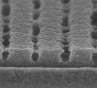

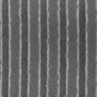
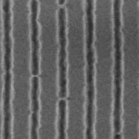

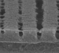
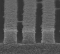
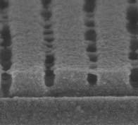
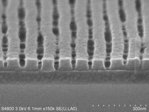
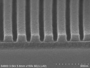
12 Issue with first resist platform, FAiRS-9101A01 Micro bridge at fine trench 45 nm trench μm μm μm B.F μm μm μm 32 nm trench P-12

13 Hypothesis of micro bridge at top of resist pattern Hypothesis 2: Swelling during development or rinse Δ Impedance, ohm Negative development 0.0 mj 1.0 mj 3.0 mj 4.0 mj 4.6 mj 5.0 mj 6.0 mj 20.0 mj Hypothesis 1: Lowered dissolution rate at surface Count of protection unit Film Surface QCM analysis Negative development rinse 100 TOF-SIMS analysis for de-blocking ratio Film Inside Depth from film surface, nm 0.0 mj 5.0 mj 10.0 mj 20.0 mj Δ Impedance, ohm Positive development 0.0 mj 2.0 mj 4.0 mj 6.0 mj 7.0 mj 8.0 mj 10.0 mj Development time, sec Development time, sec P Development time, sec
14 Surface localization properties for several PAGs Surface localization properties after PEB by ESCA method Relative acid concentration ratio indicates the ratio of the amount after PEB to that before PEB. Relative acid concentration ratio Conventional PAG PAG-C PAG-B PAG-A Some kinds of PAG showed very small concentration property at PEB step PEB Temperature P-14


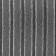
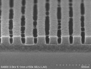
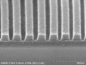
15 Improvement by suppressing acid localization at film surface 32nm Target 9521A01 Conventional PAG 9521A01A New PAG-A 9521A01B New PAG-B LWR 4.7 nm LWR 4.2 nm LWR 4.8 nm 1.2NA, dipole illumination P-15


16 Mask linearity data FAiRS-9521A01 64nm Mask 60nm Mask 56nm Mask 52nm Mask 48nm Mask 44nm Mask 1.2NA, dipole illumination 37.8 mj/sq.cm FAiRS-9521A01A 64nm Mask 60nm Mask 56nm Mask 52nm Mask 48nm Mask 44nm Mask P-16


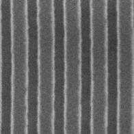
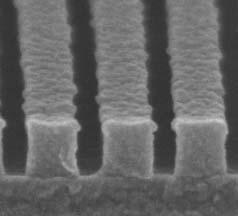
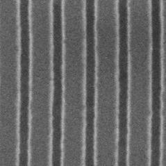
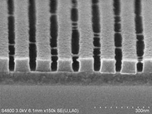
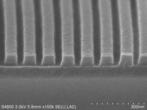
17 LWR at optimized SB/PEB condition (1.2NA, dipole condition) 32nm trench at 128nm pitch LWR = 4.1 nm Rectangle scan LWR = 2.4 nm Eop = 37 mj / cm2 Exposure latitude = 18% MEEF = 0.8 P-17


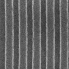
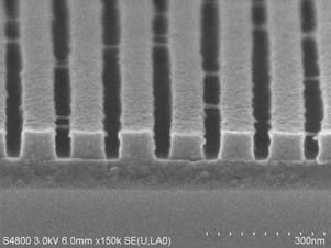
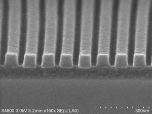
18 Resolution at optimized SB/PEB condition (1.2NA, dipole condition) 44nm trench at 88nm pitch Eop = 21 mj / cm2 Exposure latitude = 25% LWR = 4.5 nm P-18


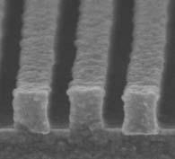
19 Dense trench performance with 1.35 NA, dipole illumination 38nm HP, 1:1 W/B mask 22 mj / cm 2 24 mj / cm 2 26 mj / cm 2 28 mj / cm 2 30 mj / cm 2 32 mj / cm 2 44 mj / cm 2 42 mj / cm 2 40 mj / cm 2 38 mj / cm 2 36 mj / cm 2 34 mj / cm 2 EL=29.2% Bridge margin: 33% Collapse margin: >36% P-19


20 Dense trench performance with 1.35 NA, dipole illumination 38nm HP, 1:1 W/B mask, 30 mj / cm μm μm μm μm Best Focus μm μm μm μm P-20
21 Outline 1. Advantages of negative tone imaging for DP 2. Resist material progress for negative tone development 3. Process maturity of negative tone development 4. Summary 5. Acknowledgement P-21
22 CD uniformity data, FAiRS-9521A01 NTD Mean CD Wafer number R9 R8 R7 R6 R5 R4 R3 R2 R1 R0 R-1 R-2 R-3 R-4 R-5 R-6 R-7 R-8 R-9 C-11 C-9 C-7 C-5 C-3 C-1 C1 C3 C5 C7 C9 C x STD-Dev Resist: FAiRS-9521A01 Developer: FN-DP001 45nm trench / 128nm pitch NA1.2, dipole illumination Dynamic dev-1 R9 R8 R7 R6 R5 R4 R3 R2 R1 R0 R-1 R-2 R-3 R-4 R-5 R-6 R-7 R-8 R-9 C-11 C-9 C-7 C-5 C-3 C-1 C1 C3 C5 C7 C9 C11 W-1 W P-22
23 CD uniformity data, FAiRS-9521A01A NTD and PTD NTD Developer: FN-DP001 Dynamic dev-1. 45nm trench 128nm pitch NA1.2 dipole illumination PTD Developer: OPD5262 Dynamic dev-2. R9 R8 R7 R6 R5 R4 R3 R2 R1 R0 R-1 R-2 R-3 R-4 R-5 R-6 R-7 R-8 R-9 C-11 C-9 C-7 C-5 C-3 C-1 C1 C3 C5 C7 C9 C11 W NTD PTD Mean 43.8 nm 42.6 nm 3 x STD dev. 3.3 nm 4.0 nm R9 R8 R7 R6 R5 R4 R3 R2 R1 R0 R-1 R-2 R-3 R-4 R-5 R-6 R-7 R-8 R-9 C-11 C-9 C-7 C-5 C-3 C-1 C1 C3 C5 C7 C9 C11 W R9 R8 R7 R6 R5 R4 R3 R2 R1 R0 R-1 R-2 R-3 R-4 R-5 R-6 R-7 R-8 R-9 C-11 C-9 C-7 C-5 C-3 C-1 C1 C3 C5 C7 C9 C11 W Mean 42.7 nm 41.2 nm 3 x STD dev. 4.2 nm 5.1 nm R9 R8 R7 R6 R5 R4 R3 R2 R1 R0 R-1 R-2 R-3 R-4 R-5 R-6 R-7 R-8 R-9 C-11 C-9 C-7 C-5 C-3 C-1 C1 C3 C5 C7 C9 C11 W P-23
24 CD uniformity and LWR uniformity with 1.35 NA NTD Developer: FN-DP001 Dynamic dev-1. frequency CD, nm 43 nm trench 90 nm pitch NA1.35 dipole illumination NTD PTD Mean 43.2 nm 43.3 nm 3 x STD dev. 1.6 nm 1.4 nm frequency PTD Developer: OPD262 Static dev CD, nm frequency LWR, nm Mean 4.8 nm 5.3 nm 3 x STD dev. 1.1 nm 1.2 nm frequency LWR, nm P-24
25 Outline 1. Advantages of negative tone imaging for DP 2. Resist material progress for negative tone development 3. Process maturity of negative tone development 4. Summary 5. Acknowledgement P-25
26 Summary 1. Advantage in trench CD uniformity of double trench process was discussed, and negative tone development (NTD) process was proposed as the best candidate for fine trench printing. 2. Micro bridge of original platform FAiRS-9521A01 is no longer critical issue by control of PAG localization after PEB at film surface. New platform FAiRS- 9521A01A was released. 3. FAiRS-9521A01A demonstrated 88 nm pitch resolution with 1.2 NA immersion exposure, and 76 nm pitch resolution with 1.35 NA immersion exposure. 4. Process maturity of NTD process was studied with CD uniformity comparison with positive tone development process. Quite promising initial results of 3-4 nm three sigma was obtained without any optimization of process. P-26
27 Acknowledgement Dr. Roel Gronheid, Dr. Mireille Maenhoudt, Dr. Joost Bekaert at IMEC. Junichi Kitano, Tsuyoshi Shibata, Kathleen Nafus, Shinichi Hatakeyama, Steven Scheer, Carlos Fonseca, Takafumi Niwa at Tokyo Electron. Grozdan Grozev, Mario Reybrouck, and Veerle Van Driessche at FUJIFILM ELECTRONIC MATERIALS (EUROPE) N.V. P-27
IMEC update. A.M. Goethals. IMEC, Leuven, Belgium
 IMEC update A.M. Goethals IMEC, Leuven, Belgium Outline IMEC litho program overview ASML ADT status 1 st imaging Tool description Resist projects Screening using interference litho K LUP / Novel resist
Holistic View of Lithography for Double Patterning. Skip Miller ASML
 Holistic View of Lithography for Double Patterning Skip Miller ASML Outline Lithography Requirements ASML Holistic Lithography Solutions Conclusions Slide 2 Shrink Continues Lithography keeps adding value
EUV Resist Materials and Process for 16 nm Half Pitch and Beyond
 EUV Workshop 2013 June 13, 2013 EUV Resist Materials and Process for 16 nm Half Pitch and Beyond Yoshi Hishiro JSR Micro Inc. No13-2400-056 Challenge for EUV Resist & JSR approaches EUV Resist Resolution,
Advanced Patterning Techniques for 22nm HP and beyond
 Advanced Patterning Techniques for 22nm HP and beyond An Overview IEEE LEOS (Bay Area) Yashesh A. Shroff Intel Corporation Aug 4 th, 2009 Outline The Challenge Advanced (optical) lithography overview Flavors
Business Unit Electronic Materials
 Frank Houlihan, Raj Sakamuri, David Rentkiewicz Andrew Romano, Ralph R. Dammel AZ Electronic Materials, Clariant Corporation, Somerville, NJ Michael Sebald, Nickolay Stepanenko, M. Markert, U. Mierau,
immersion optics Immersion Lithography with ASML HydroLith TWINSCAN System Modifications for Immersion Lithography by Bob Streefkerk
 immersion optics Immersion Lithography with ASML HydroLith by Bob Streefkerk For more than 25 years, many in the semiconductor industry have predicted the end of optical lithography. Recent developments,
Double Patterning Combined with Shrink Technique to Extend ArF Lithography for Contact Holes to 22nm Node and Beyond
 Double Patterning Combined with Shrink Technique to Extend ArF Lithography for Contact Holes to 22nm Node and Beyond Juliet Xiangqun Miao, Lior Huli b, Hao Chen, Xumou Xu, Hyungje Woo, Chris Bencher, Jen
Multiple Patterning for Immersion Extension and EUV Insertion. Chris Bencher Distinguished Member of Technical Staff Applied Materials CTO group
 Multiple Patterning for Immersion Extension and EUV Insertion Chris Bencher Distinguished Member of Technical Staff Applied Materials CTO group Abstract Multiple Patterning for Immersion Extension and
Novel EUV Resist Development for Sub-14nm Half Pitch
 EUV Workshop 2015 Maui, HI P64 Novel EUV Resist Development for Sub-14nm Half Pitch Yoshi Hishiro JSR Micro Inc. EUV Workshop, June 17, 2015 1 Contents Requirement for sub-14nm HP EUV resist JSR strategy
EUVL Scanners Operational at Chipmakers. Skip Miller Semicon West 2011
 EUVL Scanners Operational at Chipmakers Skip Miller Semicon West 2011 Outline ASML s Lithography roadmap to support Moore s Law Progress on NXE:3100 (0.25NA) EUV systems Progress on NXE:3300 (0.33NA) EUV
Lithography Simulation Tools Needed for 22nm HP and Beyond. Chris Mack
 Lithography Simulation Tools Needed for 22nm HP and Beyond Chris Mack www.lithoguru.com Slicing the Pie Simulation Tool Characteristics Precision Accuracy Capabilities (speed, features) Simulation Tool
Shooting for the 22nm Lithography Goal with the. Coat/Develop Track. SOKUDO Lithography Breakfast Forum 2010 July 14 (L1)
") Shooting for the 22nm Lithography Goal with the Coat/Develop Track SOKUDO Lithography Breakfast Forum 2010 July 14 (L1) Three (3) different exposure options for 22nm: Public External (L1) MAPPER Lithography
Shooting for the 22nm Lithography Goal with the Coat/Develop Track SOKUDO Lithography Breakfast Forum 2010 July 14 (L1) Three (3) different exposure options for 22nm: Public External (L1) MAPPER Lithography
Toward 5nm node ; Untoward Scaling with Multi-patterning
 1 st International Symposium on DSA Toward 5nm node ; Untoward Scaling with Multi-patterning 27 th OCT 2015 H. Yaegashi Chief Engineer Tokyo Electron Limited Down-caling trend towards N5 N20 N14 N10 N7
Comparative Study of Binary Intensity Mask and Attenuated Phase Shift Mask using Hyper-NA Immersion Lithography for Sub-45nm Era
 Comparative Study of Binary Intensity Mask and Attenuated Phase Shift Mask using Hyper-NA Immersion Lithogr for Sub-45nm Era Tae-Seung Eom*, Jun-Taek Park, Sarohan Park, Sunyoung Koo, Jin-Soo Kim, Byoung-Hoon
UV Nanoimprint Stepper Technology: Status and Roadmap. S.V. Sreenivasan Sematech Litho Forum May 14 th, 2008
 UV Nanoimprint Stepper Technology: Status and Roadmap S.V. Sreenivasan Sematech Litho Forum May 14 th, 2008 Overview Introduction Stepper technology status: Patterning and CD Control Through Etch Alignment
R&D Status and Key Technical and Implementation Challenges for EUV HVM
 R&D Status and Key Technical and Implementation Challenges for EUV HVM Sam Intel Corporation Agenda Requirements by Process Node EUV Technology Status and Gaps Photoresists Tools Reticles Summary 2 Moore
Beyond Immersion Patterning Enablers for the Next Decade
 Beyond Immersion Patterning Enablers for the Next Decade Colin Brodsky Manager and Senior Technical Staff Member Patterning Process Development IBM Semiconductor Research & Development Center Hopewell
Optical Lithography. Keeho Kim Nano Team / R&D DongbuAnam Semi
 Optical Lithography Keeho Kim Nano Team / R&D DongbuAnam Semi Contents Lithography = Photolithography = Optical Lithography CD : Critical Dimension Resist Pattern after Development Exposure Contents Optical
22nm node imaging and beyond: a comparison of EUV and ArFi double patterning
 22nm node imaging and beyond: a comparison of EUV and ArFi double patterning ASML: Eelco van Setten, Orion Mouraille, Friso Wittebrood, Mircea Dusa, Koen van Ingen-Schenau, Jo Finders, Kees Feenstra IMEC:
Pupil wavefront manipulation for optical nanolithography
 Pupil wavefront manipulation for optical nanolithography Monica Kempsell Sears a *, Joost Bekaert b, Bruce W. Smith a a RIT, Microsystems Engineering, 77 Lomb Memorial Drive, Rochester, NY 14623 b IMEC
Process Optimization
 Process Optimization Process Flow for non-critical layer optimization START Find the swing curve for the desired resist thickness. Determine the resist thickness (spin speed) from the swing curve and find
Lithography on the Edge
 Lithography on the Edge David Medeiros IBM Prague, Czech Republic 3 October 009 An Edge A line where an something begins or ends: A border, a discontinuity, a threshold Scaling Trend End of an Era? 0000
Development of a LFLE Double Pattern Process for TE Mode Photonic Devices. Mycahya Eggleston Advisor: Dr. Stephen Preble
 Development of a LFLE Double Pattern Process for TE Mode Photonic Devices Mycahya Eggleston Advisor: Dr. Stephen Preble 2 Introduction and Motivation Silicon Photonics Geometry, TE vs TM, Double Pattern
EUVL getting ready for volume introduction
 EUVL getting ready for volume introduction SEMICON West 2010 Hans Meiling, July 14, 2010 Slide 1 public Outline ASML s Lithography roadmap to support Moore s Law Progress on 0.25NA EUV systems Progress
TECHNOLOGY ROADMAP 2006 UPDATE LITHOGRAPHY FOR
 INTERNATIONAL TECHNOLOGY ROADMAP FOR SEMICONDUCTORS 2006 UPDATE LITHOGRAPHY THE ITRS IS DEVISED AND INTENDED FOR TECHNOLOGY ASSESSMENT ONLY AND IS WITHOUT REGARD TO ANY COMMERCIAL CONSIDERATIONS PERTAINING
Update on 193nm immersion exposure tool
 Update on 193nm immersion exposure tool S. Owa, H. Nagasaka, Y. Ishii Nikon Corporation O. Hirakawa and T. Yamamoto Tokyo Electron Kyushu Ltd. January 28, 2004 Litho Forum 1 What is immersion lithography?
From ArF Immersion to EUV Lithography
 From ArF Immersion to EUV Lithography Luc Van den hove Vice President IMEC Outline Introduction 193nm immersion lithography EUV lithography Global collaboration Conclusions Lithography is enabling 1000
Sub-12nm Optical Lithography with 4x Pitch Division and SMO-Lite
 Sub-12nm Optical Lithography with 4x Pitch Division and SMO-Lite Michael C. Smayling* a, Koichiro Tsujita b, Hidetami Yaegashi c, Valery Axelrad d Tadashi Arai b, Kenichi Oyama c, Arisa Hara c a Tela Innovations,
A Novel Resist Freeze Process for Double Imaging
 A Novel Resist Freeze Process for Double Imaging David J. Abdallah, Eric Alemy, Srinivasan Chakrapani, Munirathna Padmanaban and Ralph R. Dammel AZ Electronic Materials Somerville, NJ USA 1 st exp 2 nd
Line Width Roughness Control for EUV Patterning
 Line Width Roughness Control for EUV Patterning Shinichiro Kawakami, Lior Huli, Shannon Dunn, Akiteru Ko TEL Technology Center, America, LLC., 255 Fuller Road, STE 244, Albany, NY 12203 USA Karen Petrillo,
OPC Rectification of Random Space Patterns in 193nm Lithography
 OPC Rectification of Random Space Patterns in 193nm Lithography Mosong Cheng, Andrew Neureuther, Keeho Kim*, Mark Ma*, Won Kim*, Maureen Hanratty* Department of Electrical Engineering and Computer Sciences
Imaging for the next decade
 Imaging for the next decade Martin van den Brink Executive Vice President Products & Technology IMEC Technology Forum 2009 3 June, 2009 Slide 1 Congratulations! ASML and years of making chips better Slide
Critical issue of non-topcoat resist for ultra low k 1 lithography
 Critical issue of non-topcoat resist for ultra low k 1 lithography 1 Hirokazu Kato, 1 Tomoya Oori, 1 Koutaro Sho, 1 Kentaro Matsunaga, 1 Eishi Shiobara, 1 Tsukasa Azuma, 2 Yukio Nishimura, 2 Hiroki Nakagawa,
Key Photolithographic Outputs
 Exposure latitude Depth of Focus Exposure latitude Vs DOF plot Linearity and MEEF Isolated-Dense Bias NILS Contrast Swing Curve Reflectivity Curve 1 Exposure latitude:the range of exposure energies (usually
Double Patterning Combined with Shrink Technique to Extend ArF Lithography for Contact Holes to 22nm Node and Beyond
 Double Patterning Combined with Shrink Technique to Extend ArF Lithography for Contact Holes to 22nm Node and Beyond Xiangqun Miao* a, Lior Huli b, Hao Chen a, Xumou Xu a, Hyungje Woo a, Chris Bencher
Progresses in NIL Template Fabrication Naoya Hayashi
 Progresses in NIL Template Fabrication Naoya Hayashi Electronic Device Operations Dai Nippon Printing Co., Ltd. Contents 1. Introduction Motivation NIL mask fabrication process 2. NIL mask resolution improvement
Immersion Lithography: New Opportunities for Semiconductor Manufacturing
 Immersion Lithography: New Opportunities for Semiconductor Manufacturing Tim Brunner, Dario Gil, Carlos Fonseca and Nakgeuon Seong IBM - SRDC Bob Streefkerk, Christian Wagner and Marco Stavenga ASML Outline
Lithography Roadmap. without immersion lithography. Node Half pitch. 248nm. 193nm. 157nm EUVL. 3-year cycle: 2-year cycle: imec 2005
 Lithography Roadmap without immersion lithography Node Half pitch 180 nm 130 nm 90 nm 65 nm 45 nm 32 nm 22 nm 250 nm 180 nm 130 nm 90 nm 65 nm 45 nm 32 nm 248nm 193nm 157nm EUVL 3-year cycle: 2-year cycle:
450mm patterning out of darkness Backend Process Exposure Tool SOKUDO Lithography Breakfast Forum July 10, 2013 Doug Shelton Canon USA Inc.
 450mm patterning out of darkness Backend Process Exposure Tool SOKUDO Lithography Breakfast Forum 2013 July 10, 2013 Doug Shelton Canon USA Inc. Introduction Half Pitch [nm] 2013 2014 2015 2016 2017 2018
Light Source Technology Advances to Support Process Stability and Performance Predictability for ArF Immersion Double Patterning
 Light Source Technology Advances to Support Process Stability and Performance Predictability for ArF Immersion Double Patterning Ivan Lalovic, Rajasekhar Rao, Slava Rokitski, John Melchior, Rui Jiang,
Evaluation of Technology Options by Lithography Simulation
 Evaluation of Technology Options by Lithography Simulation Andreas Erdmann Fraunhofer IISB, Erlangen, Germany Semicon Europe, Dresden, October 12, 2011 Outline Introduction: Resolution limits of optical
2008 European EUVL. EUV activities the EUVL shop future plans. Rob Hartman
 2008 European EUVL EUV activities the EUVL shop future plans Rob Hartman 2007 international EUVL Symposium 28-31 October 2007 2008 international EUVL Symposium 28 Sapporo, September Japan 1 October 2008
Section 2: Lithography. Jaeger Chapter 2 Litho Reader. The lithographic process
 Section 2: Lithography Jaeger Chapter 2 Litho Reader The lithographic process Photolithographic Process (a) (b) (c) (d) (e) (f) (g) Substrate covered with silicon dioxide barrier layer Positive photoresist
The future of EUVL. Outline. by Winfried Kaiser, Udo Dinger, Peter Kuerz, Martin Lowisch, Hans-Juergen Mann, Stefan Muellender,
 The future of EUVL by Winfried Kaiser, Udo Dinger, Peter Kuerz, Martin Lowisch, Hans-Juergen Mann, Stefan Muellender, William H. Arnold, Jos Benshop, Steven G. Hansen, Koen van Ingen-Schenau Outline Introduction
EUV Interference Lithography in NewSUBARU
 EUV Interference Lithography in NewSUBARU Takeo Watanabe 1, Tae Geun Kim 2, Yasuyuki Fukushima 1, Noki Sakagami 1, Teruhiko Kimura 1, Yoshito Kamaji 1, Takafumi Iguchi 1, Yuuya Yamaguchi 1, Masaki Tada
Nikon EUVL Development Progress Update
 Nikon EUVL Development Progress Update Takaharu Miura EUVL Symposium September 29, 2008 EUVL Symposium 2008 @Lake Tahoe T. Miura September 29, 2008 Slide 1 Presentation Outline 1. Nikon EUV roadmap 2.
Anti-reflective coating for multipatterning lithography
 Anti-reflective coating for multipatterning lithography Douglas J. Guerrero, Steve Gibbons, Joyce Lowes, Ramil Mercado Brewer Science, Inc., 2401 Brewer Drive, Rolla, MO 65401, USA ABSTRACT New bottom
Section 2: Lithography. Jaeger Chapter 2 Litho Reader. EE143 Ali Javey Slide 5-1
 Section 2: Lithography Jaeger Chapter 2 Litho Reader EE143 Ali Javey Slide 5-1 The lithographic process EE143 Ali Javey Slide 5-2 Photolithographic Process (a) (b) (c) (d) (e) (f) (g) Substrate covered
Simulation of Quartz phase etch affect on performance of ArF chrome-less hard shifter for 65-nm technology
 Simulation of Quartz phase etch affect on performance of ArF chrome-less hard shifter for 65-nm technology KT Park*, Martin Sczyrba**, Karsten Bubke**, Rainer Pforr*** (*) DPI assignee at AMTC GmbH & Co.
Status and challenges of EUV Lithography
 Status and challenges of EUV Lithography SEMICON Europa Dresden, Germany Jan-Willem van der Horst Product Manager EUV October 10 th, 2013 Slide 2 Contents Introduction NXE:3100 NXE:3300B Summary and acknowledgements
PUSHING LITHOGRAPHY TO ENABLE ULTIMATE NANO-ELECTRONICS. LUC VAN DEN HOVE President & CEO imec
 PUSHING LITHOGRAPHY TO ENABLE ULTIMATE NANO-ELECTRONICS LUC VAN DEN HOVE President & CEO imec OUTLINE! Industry drivers! Roadmap extension! Lithography options! Innovation through global collaboration
Impact of 3-D Mask Effects on CD and Overlay over Image Field in Extreme Ultraviolet Lithography
 Impact of 3-D Mask Effects on CD and Overlay over Image Field in Extreme Ultraviolet Lithography 5 th International EUV Symposium Barcelona, Spain Sven Trogisch Markus Bender Frank-Michael Kamm Disclaimer
MeRck. AZ nlof technical datasheet. Negative Tone Photoresist for Single Layer Lift-Off APPLICATION TYPICAL PROCESS. SPIN CURVE (150MM Silicon)
") MeRck technical datasheet AZ nlof 5510 Negative Tone Photoresist for Single Layer Lift-Off APPLICATION AZ nlof 5510 i-line photoresist is engineered to simplify the historically complex image reversal
MeRck technical datasheet AZ nlof 5510 Negative Tone Photoresist for Single Layer Lift-Off APPLICATION AZ nlof 5510 i-line photoresist is engineered to simplify the historically complex image reversal
Copyright 2000, Society of Photo-Optical Instrumentation Engineers This paper was published in Optical Microlithography XIII, Volume 4000 and is made
 Copyright 00, Society of Photo-Optical Instrumentation Engineers This paper was published in Optical Microlithography XIII, Volume 4000 and is made available as an electronic reprint with permission of
Lithography. Development of High-Quality Attenuated Phase-Shift Masks
 Lithography S P E C I A L Development of High-Quality Attenuated Phase-Shift Masks by Toshihiro Ii and Masao Otaki, Toppan Printing Co., Ltd. Along with the year-by-year acceleration of semiconductor device
Status and Challenges for Multibeam DW lithography. L. PAIN CEA - LETI Silicon Technology Department
 Status and Challenges for Multibeam DW lithography L. PAIN CEA - LETI Silicon Technology Department Outline Introduction Challenges Current program status KLA-TENCOR MAPPER Demonstration capability IMAGINE
Design Rules for Silicon Photonics Prototyping
 Design Rules for licon Photonics Prototyping Version 1 (released February 2008) Introduction IME s Photonics Prototyping Service offers 248nm lithography based fabrication technology for passive licon-on-insulator
Photolithography I ( Part 1 )
") 1 Photolithography I ( Part 1 ) Chapter 13 : Semiconductor Manufacturing Technology by M. Quirk & J. Serda Bjørn-Ove Fimland, Department of Electronics and Telecommunication, Norwegian University of Science
1 Photolithography I ( Part 1 ) Chapter 13 : Semiconductor Manufacturing Technology by M. Quirk & J. Serda Bjørn-Ove Fimland, Department of Electronics and Telecommunication, Norwegian University of Science
Pattern Transfer CD-AFM. Resist Features on Poly. Poly Features on Oxide. Quate Group, Stanford University
 Resist Features on Poly Pattern Transfer Poly Features on Oxide CD-AFM The Critical Dimension AFM Boot -Shaped Tip Tip shape is optimized to sense topography on vertical surfaces Two-dimensional feedback
Optimizing FinFET Structures with Design-based Metrology
 Lithography M e t r o l o g y Optimizing FinFET Structures with Design-based Metrology Tom Vandeweyer, Christie Delvaux, Johan De Backer, and Monique Ercken, IMEC Gian Lorusso, Radhika Jandhyala, Amir
EUV: Status and Challenges Ahead International Workshop on EUVL, Maui 2010
 EUV: Status and Challenges Ahead International Workshop on EUVL, Maui 2010 Jos Benschop Public Agenda Roadmap Status Challenges Summary & conclusion Slide 2 Public Resolution (half pitch) "Shrink" [nm]
Templates, DTR and BPM Media
 Complete Metrology Solutions Imprint Technology Templates, DTR and BPM Media Simultaneous and Non-Destructive Measurements of Depth Top and Bottom CD Residual Layer Thickness, RLT DLC Thickness Side Wall
Characterization of a Thick Copper Pillar Bump Process
 Characterization of a Thick Copper Pillar Bump Process Warren W. Flack, Ha-Ai Nguyen Ultratech, Inc. San Jose, CA 95126 Elliott Capsuto, Craig McEwen Shin-Etsu MicroSi, Inc. Phoenix, AZ 85044 Abstract
Decomposition difficulty analysis for double patterning and. the impact on photomask manufacturability
 Decomposition difficulty analysis for double patterning and the impact on photomask manufacturability Yuichi Inazuki 1*, Nobuhito Toyama, Takaharu Nagai 1, Takanori Sutou 1, Yasutaka Morikawa 1, Hiroshi
Atlas 46 novel negative tone photoresist which combines the good properties of the established SU-8 and CAR 44
 EIPBN, 30 th Mai 2018 Atlas 46 novel negative tone photoresist which combines the good properties of the established SU-8 and CAR 44 Dr. Christian Kaiser, Matthias Schirmer Allresist GmbH, Germany Outline
EE143 Fall 2016 Microfabrication Technologies. Lecture 3: Lithography Reading: Jaeger, Chap. 2
 EE143 Fall 2016 Microfabrication Technologies Lecture 3: Lithography Reading: Jaeger, Chap. 2 Prof. Ming C. Wu wu@eecs.berkeley.edu 511 Sutardja Dai Hall (SDH) 1-1 The lithographic process 1-2 1 Photolithographic
Optical Microlithography XXVIII
 PROCEEDINGS OF SPIE Optical Microlithography XXVIII Kafai Lai Andreas Erdmann Editors 24-26 February 2015 San Jose, California, United States Sponsored by SPIE Cosponsored by Cymer, an ASML company (United
Organic Antireflective Coatings for Photomask Fabrication using Optical Pattern Generators
 Organic Antireflective Coatings for Photomask Fabrication using Optical Pattern Generators Benjamen M. Rathsack 1, Cyrus E. Tabery 1, Cece Philbin 2, and C. Grant Willson 1 September 15, 1999 1 Department
EUV lithography: today and tomorrow
 EUV lithography: today and tomorrow Vadim Banine, Stuart Young, Roel Moors Dublin, October 2012 Resolution/half pitch, "Shrink" [nm] EUV DPT ArFi ArF KrF Industry roadmap towards < 10 nm resolution Lithography
Double Exposure Using 193nm Negative Tone Photoresist
 Double Exposure Using 193nm Negative Tone Photoresist Ryoung-han Kim a, Tom Wallow a, Jongwook Kye a, Harry J. Levinson a, and Dave White b a Advanced Micro Devices, One AMD Place, Sunnyvale, CA 94088,
Competitive in Mainstream Products
 Competitive in Mainstream Products Bert Koek VP, Business Unit manager 300mm Fabs Analyst Day 20 September 2005 ASML Competitive in mainstream products Introduction Market share Device layers critical
EUVL: Challenges to Manufacturing Insertion
 EUVL: Challenges to Manufacturing Insertion Obert R Wood II International Workshop on EUV Lithography CXRO, LBNL, Berkeley, California 14 June 2017 EUV Critical Issues List EUV Critical Issues, as identified
5 th Annual ebeam Initiative Luncheon SPIE February 26, Aki Fujimura CEO D2S, Inc. Managing Company Sponsor ebeam Initiative
 5 th Annual ebeam Initiative Luncheon SPIE February 26, 2013 Aki Fujimura CEO D2S, Inc. Managing Company Sponsor ebeam Initiative ebeam Writes All Chips The ebeam Initiative: Is an educational platform
MeRck. nlof 2000 Series. technical datasheet. Negative Tone Photoresists for Single Layer Lift-Off APPLICATION TYPICAL PROCESS
 MeRck technical datasheet AZ Negative Tone Photoresists for Single Layer Lift-Off APPLICATION AZ i-line photoresists are engineered to simplify the historically complex image reversal and multilayer lift-off
Micro Photonics, Berlin
 Imprint Nanopatterning Solution Platform for IndustRial assessment NANO IMPRINT LITHOGRAPHY (NIL) FOR PHOTONICS APPLICATIONS Hubert TEYSSEDRE Stefan LANDIS Sandra BOS Laurent PAIN Yannick LE TIEC LETI,
A Reliable Higher Power ArF Laser with Advanced Functionality for Immersion Lithography
 A Reliable Higher Power ArF Laser with Advanced Functionality for Immersion Lithography Akihiko Kurosu, Masaki Nakano, Masanori Yashiro, Masaya Yoshino, Hiroaki Tsushima, Hiroyuki Masuda, Takahito Kumazaki,
Application-Based Opportunities for Reused Fab Lines
 Application-Based Opportunities for Reused Fab Lines Semicon China, March 17 th 2010 Keith Best Simax Lithography S I M A X A L L I A N C E P A R T N E R S Outline Market: Exciting More than Moore applications
DSA and 193 immersion lithography
 NIKON RESEARCH CORP. OF AMERICA DSA and 193 immersion lithography Steve Renwick Senior Research Scientist, Imaging Sol ns Technology Development Where the industry wants to go 2 Where we are now 193i e-beam
Resist Process Window Characterization for the 45-nm Node Using an Interferometric Immersion microstepper
 Rochester Institute of Technology RIT Scholar Works Presentations and other scholarship 3-29-2006 Resist Process Window Characterization for the 45-nm Node Using an Interferometric Immersion microstepper
Next-generation DUV light source technologies for 10nm and below
 Next-generation DUV light source technologies for 10nm and below Ted Cacouris, Greg Rechtsteiner, Will Conley Cymer LLC, 17075 Thornmint Court, San Diego, CA 92127 ABSTRACT Multi-patterning techniques
16nm with 193nm Immersion Lithography and Double Exposure
 16nm with 193nm Immersion Lithography and Double Exposure Valery Axelrad, Sequoia Design Systems, Inc. (United States) Michael C. Smayling, Tela Innovations, Inc. (United States) ABSTRACT Gridded Design
MICRO AND NANOPROCESSING TECHNOLOGIES
 MICRO AND NANOPROCESSING TECHNOLOGIES LECTURE 4 Optical lithography Concepts and processes Lithography systems Fundamental limitations and other issues Photoresists Photolithography process Process parameter
Imec pushes the limits of EUV lithography single exposure for future logic and memory
 Edition March 2018 Semiconductor technology & processing Imec pushes the limits of EUV lithography single exposure for future logic and memory Imec has made considerable progress towards enabling extreme
2009 International Workshop on EUV Lithography
 Contents Introduction Absorber Stack Optimization Non-flatness Correction Blank Defect and Its Mitigation Wafer Printing Inspection Actinic Metrology Cleaning and Repair Status Remaining Issues in EUV
Major Fabrication Steps in MOS Process Flow
 Major Fabrication Steps in MOS Process Flow UV light Mask oxygen Silicon dioxide photoresist exposed photoresist oxide Silicon substrate Oxidation (Field oxide) Photoresist Coating Mask-Wafer Alignment
Feature-level Compensation & Control
 Feature-level Compensation & Control 2 Sensors and Control Nathan Cheung, Kameshwar Poolla, Costas Spanos Workshop 11/19/2003 3 Metrology, Control, and Integration Nathan Cheung, UCB SOI Wafers Multi wavelength
A process for, and optical performance of, a low cost Wire Grid Polarizer
 1.0 Introduction A process for, and optical performance of, a low cost Wire Grid Polarizer M.P.C.Watts, M. Little, E. Egan, A. Hochbaum, Chad Jones, S. Stephansen Agoura Technology Low angle shadowed deposition
Computational Lithography Requirements & Challenges for Mask Making. Naoya Hayashi, Dai Nippon Printing Co., Ltd
 Computational Lithography Requirements & Challenges for Mask Making Naoya Hayashi, Dai Nippon Printing Co., Ltd Contents Introduction Lithography Trends Computational lithography options More Complex OPC
Photolithography Technology and Application
 Photolithography Technology and Application Jeff Tsai Director, Graduate Institute of Electro-Optical Engineering Tatung University Art or Science? Lind width = 100 to 5 micron meter!! Resolution = ~ 3
Section 2: Lithography. Jaeger Chapter 2. EE143 Ali Javey Slide 5-1
 Section 2: Lithography Jaeger Chapter 2 EE143 Ali Javey Slide 5-1 The lithographic process EE143 Ali Javey Slide 5-2 Photolithographic Process (a) (b) (c) (d) (e) (f) (g) Substrate covered with silicon
TECHNOLOGY ROADMAP 2011 EDITION LITHOGRAPHY FOR
 INTERNATIONAL TECHNOLOGY ROADMAP FOR SEMICONDUCTORS 2011 EDITION LITHOGRAPHY THE ITRS IS DEVISED AND INTENDED FOR TECHNOLOGY ASSESSMENT ONLY AND IS WITHOUT REGARD TO ANY COMMERCIAL CONSIDERATIONS PERTAINING
Eun-Jin Kim, GukJin Kim, Seong-Sue Kim*, Han-Ku Cho*, Jinho Ahn**, Ilsin An, and Hye-Keun Oh
 Eun-Jin Kim, GukJin Kim, Seong-Sue Kim*, Han-Ku Cho*, Jinho Ahn**, Ilsin An, and Hye-Keun Oh Lithography Lab. Department of Applied Physics, Hanyang University, Korea *Samsung Electronics Co., LTD. Korea
Purpose: Explain the top 10 phenomena and concepts. BPP-1: Resolution and Depth of Focus (1.5X)
") Basic Projection Printing (BPP) Modules Purpose: Explain the top 10 phenomena and concepts key to understanding optical projection printing BPP-1: Resolution and Depth of Focus (1.5X) BPP-2: Bragg condition
Basic Projection Printing (BPP) Modules Purpose: Explain the top 10 phenomena and concepts key to understanding optical projection printing BPP-1: Resolution and Depth of Focus (1.5X) BPP-2: Bragg condition
ECSE 6300 IC Fabrication Laboratory Lecture 3 Photolithography. Lecture Outline
 ECSE 6300 IC Fabrication Laboratory Lecture 3 Photolithography Prof. James J. Q. Lu Bldg. CII, Rooms 6229 Rensselaer Polytechnic Institute Troy, NY 12180 Tel. (518)276 2909 e mails: luj@rpi.edu http://www.ecse.rpi.edu/courses/s18/ecse
Optical Projection Printing and Modeling
 Optical Projection Printing and Modeling Overview of optical lithography, concepts, trends Basic Parameters and Effects (1-14) Resolution Depth of Focus; Proximity, MEEF, LES Image Calculation, Characterization
Aerial image based mask defect detection in dense array structures
 Aerial image based mask defect detection in dense array structures Roderick Köhle a, Mario Hennig b, Rainer Pforr b, Karsten Bubke c, Martin Szcyrba c, Arndt C. Dürr c a Infineon Technologies AG, Balanstr.
Optolith 2D Lithography Simulator
 2D Lithography Simulator Advanced 2D Optical Lithography Simulator 4/13/05 Introduction is a powerful non-planar 2D lithography simulator that models all aspects of modern deep sub-micron lithography It
Optical Maskless Lithography - OML
 Optical Maskless Lithography - OML Kevin Cummings 1, Arno Bleeker 1, Jorge Freyer 2, Jason Hintersteiner 1, Karel van der Mast 1, Tor Sandstrom 2 and Kars Troost 1 2 1 slide 1 Outline Why should you consider
Flare compensation in EUV lithography
 Flare compensation in EUV lithography Place your image on top of this gray box. If no graphic is applicable, delete gray box and notch-out behind gray box, from the Title Master Jonathan Cobb, Ruiqi Tian,
Module 11: Photolithography. Lecture 14: Photolithography 4 (Continued)
") Module 11: Photolithography Lecture 14: Photolithography 4 (Continued) 1 In the previous lecture, we have discussed the utility of the three printing modes, and their relative advantages and disadvantages.
Module 11: Photolithography Lecture 14: Photolithography 4 (Continued) 1 In the previous lecture, we have discussed the utility of the three printing modes, and their relative advantages and disadvantages.