It s Time for 300mm Prime
|
|
|
- Gary Day
- 5 years ago
- Views:
Transcription


1 It s Time for 300mm Prime Iddo Hadar Managing Director, 300mm Prime Program Office SEMI Strategic Business Conference Napa Valley, California Tuesday, April 24, 2007
2 Safe Harbor Statement This presentation contains forward-looking statements, including those relating to the outlook for the semiconductor industry and R&D investment. These statements are subject to known and unknown risks and uncertainties that could cause actual results to differ materially from those expressed or implied by such statements including, without limitation: the sustainability of demand in the semiconductor and semiconductor equipment industries, which is subject to many factors, including global economic conditions, business spending, consumer confidence, demand for electronic products and integrated circuits, and geopolitical uncertainties; customers capacity requirements, including capacity utilizing the latest technology; the timing, rate, amount and sustainability of capital spending for new technology, such as 300mm and sub- 100 nanometer applications; and other risks described in Applied Materials SEC filings on Forms 10-K, 10-Q and 8-K. All forward-looking statements are based on management s estimates, projections and assumptions as of April 24, 2007, and Applied Materials undertakes no obligation to update any such statements. 2
3 Consumerization of Semiconductors Non- Consumer 58% Consumer 42% Non- Consumer 43% Consumer 57% 2000 $223B 2010F $326B Source: Gartner Dataquest 3
4 Consumerization of the Industry Changes Everything Push for advanced technology created fab challenges: High variability in tool operational performance (defects, MTBF, MTBI, MTTR) Fabs incur high costs to contain and control variability Fabs sacrifice cycle time to maintain operational efficiency This is NO LONGER ACCEPTABLE in the consumer era: Cycle time / agility requirements Cost Consumer era also severely curtails available funding across the semiconductor food chain No more Business As Usual 4
5 Fulfilling Moore s Law Cost ($) Wafer Reduce annual Operating Costs Moore s Law Cost ($) Function Manufacturing Efficiency Technology Innovation Cost ($) Area (cm 2 ) Area (cm 2 ) Wafer Reduce Time to Money, Reduce Ramp -up up time Time Reduce cycle time to Order, Install, Qual and Ramp Up Increase Good Wafer Output Increase yield # of transistors Area (cm 2 ) Wafer Size Conversions Courtesy: Sematech mm(NO) Moore s Law Requires Continual Improvement in Cost/Function which Is Driven by Technology Innovations and Manufacturing Ref: 2003 ITRS 5
6 Economic Impact of Wafer Size Transition Manufacturing Cost Trend Mfrg Costs ($/Cm 2 ) mm 300mm Note: Year 3 of production, Leading Edge Memory Source: Applied analysis of ISMI s Economic Model Technology Generation (nm) 6
7 Managing Variability Product + Process Variability Higher TPT Equipment Higher Capacity Fab Consumer Era Needs??? Larger Wafer 200mm 300mm transition What s Next? 7
8 Productivity Space 100% 80% Cycle Time (Days per Mask Layer, normalized) 60% 40% 20% Next-Generation Fab 300mm 0% 75% 100% 125% 150% 175% 200% CoO ($ per Mask Layer, normalized) 8
9 300mm Investment May NEVER Be Repaid Recouping the Industry s 300mm Investment Time for Industry to Break Even (years) $0 $10 $20 $30 Total Industry Investment ($ B) Assumptions: Semiconductor industry trending from about $200B at 8% p.a.; 300mm follows a 30-year life cycle, peaking at 50% of silicon area processed (implicitly assuming larger wafer generations); semiconductor companies enjoy 45% gross margin; 55% of semiconductor costs are in wafer fabrication; 30% of die costs can be reduced via 300mm adoption; initial investment is distributed evenly over a six-year period; cost of capital is 20% 9
10 Equipment R&D Gap $16 $12 Historical R&D Spending Projected R&D Demand (200/300mm only) Affordable R&D Forecast R&D ($B) $8 $4 >$20B Short By 2012 $0 '86 '88 '90 '92 '94 '96 '98 '00 '02 '04 '06E '08F '10F Note: Affordable R/D forecast assumes 14% of equipment industry revenues Sources: S&P, SIA, SEMI, Infrastructure Advisors 10
11 Productivity Axis 300mm Prime: an evolutionary transition to 450 mm concept 450mm 300mm 300mm Driven mostly by himix business drivers and adopters Today Next several years mm Prime - strongly influenced by new/emerging business models (high-mix, smaller order sizes, shorter product life cycles ) Time axis 11
12 12

13 Source: ISMI, Scott Kramer, 11/6/
 Wafer Size")
14 Fulfilling Moore s Law Via 300mm Prime Cost ($) Wafer Reduce annual Operating Costs Moore s Law Cost ($) Function Manufacturing Efficiency Technology Innovation Cost ($) Area (cm 2 ) Area (cm 2 ) Wafer Reduce Time to Money, Reduce Ramp -up up time Time Reduce cycle time to Order, Install, Qual and Ramp Up Increase Good Wafer Output Increase yield # of transistors Area (cm 2 ) Wafer Size Conversions Courtesy: Sematech mm(NO) Moore s Law Requires Continual Improvement in Cost/Function which Is Driven by Technology Innovations and Manufacturing Ref: 2003 ITRS 14
15 Maximizing the Return on Fab Investment Optimize fab operations PRIME Small-lot Manufacturing High Mix, Short Tight Life Equipment Cycle, Consumer-Driven Characterization/ Intelligent Demand Systems Control Universal Single-wafer Processing Build foundation of rapid, differentiated, technology solutions Extend Litho Enable transistor performance Scale interconnect RC Scale memory density (strain) Resolve nano defects 15
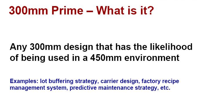
16 300mm Prime : Maximizing the Return on 300mm Investment Definition: The 300 mm Prime program seeks to implement discontinuous improvements in fab productivity of the type historically coinciding with wafer size transitions without incurring the costs and risks associated with a scale-up of tool sets Scope: primary focus will be increased fab agility and reduced cycle time, as a complement to continuous improvements in the productivity of the 300mm tool set Key levers: High-capacity, high-reliability material delivery system small-lot manufacturing Intelligent tools (high predictability) Universal single-wafer processing 16
17 Mapping 300mm Prime First Wafer Effect Needs/Benefits/Levers Tool Variability Transport & Storage Average setup time time to start processing 1 st wafer % of down time that is unscheduled Variability of time between down time Variability of repair time Wafer wait time at tool inside carrier Variability of carrier delivery time Variability (distribution) of WIP awaiting tool Possible Technological Implementations (Example) Small Carrier Size Single Wafer Processing Wafer Level Tracking 17
18 System Products Service Products Software Products 300mm Prime Architecture Processing Platforms Automation Platforms Software Platforms Universal Single-Wafer Processing Small-Lot Handling Embedded Intelligence/ Reduced Variability 18
19 Consumerization of the Industry Changes Everything Business as Usual Sacrificing fab agility Suboptimal (low-roi) investment decisions is NO LONGER ACCEPTABLE in the consumer era Cycle time / agility requirements Resource limitations Fabs need to match the economics of the consumer era Reconfigure tools to enable short cycle time manufacturing and short lead time Small lot size Frequent recipe change 19

20 20
Advancing Industry Productivity
 Advancing Industry Productivity Iddo Hadar Joint Productivity Working Group Session Austin, Texas Thursday, October 12, 2006 F O U N D A T I O N E N G I N E E R I N G G R O U P Safe Harbor Statement This
SEMI/Equipment Suppliers Productivity Working Group 450 mm Economic Findings and Conclusions
 SEMI PAPER SPONSORED AND F UNDED BY SEMI INTRODUCTION 1 BACKGROUND 1 INDUSTRY PRIORITIES 1 There Is No Imminent Productivity Crisis 1 Limitations on R&D Resources Require 2 Making Choices Cycle Time Reduction
450mm silicon wafers specification challenges. Mike Goldstein Intel Corp.
 450mm silicon wafers specification challenges Mike Goldstein Intel Corp. Outline Background 450mm transition program 450mm silicon evolution Mechanical grade wafers (spec case study) Developmental (test)
W ith development risk fully borne by the equipment industry and a two-year delay in the main
 Page 1 of 5 Economic Challenges and Opportunities in the 300 mm Transition Iddo Hadar, Jaim Nulman, Kunio Achiwa, and Oded Turbahn, Applied Materials Inc. -- 10/1/1998 Semiconductor International W ith
1 Digital EE141 Integrated Circuits 2nd Introduction
 Digital Integrated Circuits Introduction 1 What is this lecture about? Introduction to digital integrated circuits + low power circuits Issues in digital design The CMOS inverter Combinational logic structures
Introduction. Digital Integrated Circuits A Design Perspective. Jan M. Rabaey Anantha Chandrakasan Borivoje Nikolic. July 30, 2002
 Digital Integrated Circuits A Design Perspective Jan M. Rabaey Anantha Chandrakasan Borivoje Nikolic Introduction July 30, 2002 1 What is this book all about? Introduction to digital integrated circuits.
Silicon Wafer Demand Forecast Update, 4Q03
 Forecast Analysis Silicon Wafer Demand Forecast Update, 4Q03 Abstract: Silicon wafer demand in 2003 will register an 8 percent increase over 2002. Demand will enter an expansion phase in the second quarter
ISMI Industry Productivity Driver
 SEMATECH Symposium Japan September 15, 2010 Accelerating Manufacturing Productivity ISMI Industry Productivity Driver Scott Kramer VP Manufacturing Technology SEMATECH Copyright 2010 SEMATECH, Inc. SEMATECH,
Competitive in Mainstream Products
 Competitive in Mainstream Products Bert Koek VP, Business Unit manager 300mm Fabs Analyst Day 20 September 2005 ASML Competitive in mainstream products Introduction Market share Device layers critical
2010 IRI Annual Meeting R&D in Transition
 2010 IRI Annual Meeting R&D in Transition U.S. Semiconductor R&D in Transition Dr. Peter J. Zdebel Senior VP and CTO ON Semiconductor May 4, 2010 Some Semiconductor Industry Facts Founded in the U.S. approximately
Bank of America Merrill Lynch Taiwan, Technology and Beyond Conference
 Bank of America Merrill Lynch Taiwan, Technology and Beyond Conference Craig De Young Vice President Investor Relations Taipei, Taiwan March 12, 2013 Forward looking statements Slide 2 Safe Harbor Statement
Semiconductor and LED Markets. Jon Sabol Vice President and General Manager Semiconductor and LED Division
 Semiconductor and LED Markets Jon Sabol Vice President and General Manager Semiconductor and LED Division Semiconductor & LED Investing in Semiconductor and LED $ Millions 300 200 27% CAGR 100 0 * FY06
DUV. Matthew McLaren Vice President Program Management, DUV. 24 November 2014
 DUV Matthew McLaren Vice President Program Management, DUV 24 Forward looking statements This document contains statements relating to certain projections and business trends that are forward-looking,
ASML Market dynamics. Dave Chavoustie EVP Sales Analyst Day, September 30, 2004
 ASML Market dynamics Dave Chavoustie EVP Sales Analyst Day, September 30, 2004 Agenda! Market Overview! Growth Opportunities! 300mm Market! Asia Overview / Slide 2 ASML Unit Market Share Trend 60% 12 &
Update: SOI Wafer Market Continues Its Growth
 Gartner Dataquest Alert Update: SOI Wafer Market Continues Its Growth The results of Gartner Dataquest's latest survey of the silicon on insulator (SOI) wafer market indicate demand grew 16 percent in
PC accounts for 353 Cory will be created early next week (when the class list is completed) Discussions & Labs start in Week 3
 Discussions & Labs start in Week 3") EE141 Fall 2005 Lecture 2 Design Metrics Admin Page Everyone should have a UNIX account on Cory! This will allow you to run HSPICE! If you do not have an account, check: http://www-inst.eecs.berkeley.edu/usr/
EE141 Fall 2005 Lecture 2 Design Metrics Admin Page Everyone should have a UNIX account on Cory! This will allow you to run HSPICE! If you do not have an account, check: http://www-inst.eecs.berkeley.edu/usr/
The SEMATECH Model: Potential Applications to PV
 Continually cited as the model for a successful industry/government consortium Accelerating the next technology revolution The SEMATECH Model: Potential Applications to PV Dr. Michael R. Polcari President
Intel's 65 nm Logic Technology Demonstrated on 0.57 µm 2 SRAM Cells
 Intel's 65 nm Logic Technology Demonstrated on 0.57 µm 2 SRAM Cells Mark Bohr Intel Senior Fellow Director of Process Architecture & Integration Intel 1 What are We Announcing? Intel has fabricated fully-functional
Semiconductor Industry Perspective
 Semiconductor Industry Perspective National Academy of Engineering Workshop on the Offshoring of Engineering Washington, D.C. October 25, 2006 Dr. Robert Doering Texas Instruments, Inc. A Few Introductory
Jan M. Rabaey Anantha Chandrakasan Borivoje Nikolic. July 30, Digital EE141 Integrated Circuits 2nd Introduction
 Digital Integrated Circuits A Design Perspective Jan M. Rabaey Anantha Chandrakasan Borivoje Nikolic Introduction July 30, 2002 1 What is this book all about? Introduction to digital integrated circuits.
3Q03 Silicon Wafer Update: Demand Continues Recovery
 Gartner Dataquest Alert 3Q03 Silicon Wafer Update: Demand Continues Recovery The latest silicon forecast indicates that silicon wafer demand will grow 10 percent in 2003 over the previous year. This is
4Q02 Update: Semiconductor Capacity Still on Hold
 Research Brief 4Q02 Update: Semiconductor Capacity Still on Hold Abstract: Semiconductor capacity expansions have gone into a hold mode as soft semiconductor demand drops utilization rates lower. Further
Manufacturing Case Studies: Copy Exactly (CE!) and the two-year cycle at Intel
 and the two-year cycle at Intel") Manufacturing Case Studies: Copy Exactly (CE!) and the two-year cycle at Intel Paolo A. Gargini Director Technology Strategy Intel Fellow 1 Agenda 2-year cycle Copy Exactly Conclusions 2 I see no reason
Manufacturing Case Studies: Copy Exactly (CE!) and the two-year cycle at Intel Paolo A. Gargini Director Technology Strategy Intel Fellow 1 Agenda 2-year cycle Copy Exactly Conclusions 2 I see no reason
Recent Trends in Semiconductor IC Device Manufacturing
 Recent Trends in Semiconductor IC Device Manufacturing August 2007 Dr. Stephen Daniels Executive Director National Centre for Plasma Moore s Law Moore s First Law Chip Density will double ever 18months.
Market and technology trends in advanced packaging
 Close Market and technology trends in advanced packaging Executive OVERVIEW Recent advances in device miniaturization trends have placed stringent requirements for all aspects of product manufacturing.
Trends and Challenges in VLSI Technology Scaling Towards 100nm
 Trends and Challenges in VLSI Technology Scaling Towards 100nm Stefan Rusu Intel Corporation stefan.rusu@intel.com September 2001 Stefan Rusu 9/2001 2001 Intel Corp. Page 1 Agenda VLSI Technology Trends
EUV Supporting Moore s Law
 EUV Supporting Moore s Law Marcel Kemp Director Investor Relations - Europe DB 2014 TMT Conference London September 4, 2014 Forward looking statements This document contains statements relating to certain
Intel Demonstrates High-k + Metal Gate Transistor Breakthrough on 45 nm Microprocessors
 Intel Demonstrates High-k + Metal Gate Transistor Breakthrough on 45 nm Microprocessors Mark Bohr Intel Senior Fellow Logic Technology Development Kaizad Mistry 45 nm Program Manager Logic Technology Development
21 st Annual Needham Growth Conference
 21 st Annual Needham Growth Conference Investor Presentation January 15, 2019 Safe Harbor Statement The information contained in and discussed during this presentation may include forward-looking statements
Intel Technology Journal
 Volume 06 Issue 02 Published, May 16, 2002 ISSN 1535766X Intel Technology Journal Semiconductor Technology and Manufacturing The Intel Lithography Roadmap A compiled version of all papers from this issue
The Development of the Semiconductor CVD and ALD Requirement
 The Development of the Semiconductor CVD and ALD Requirement 1 Linx Consulting 1. We create knowledge and develop unique insights at the intersection of electronic thin film processes and the chemicals
ISMI 450mm Transition Program
 SEMATECH Symposium Taiwan September 7, 2010 Accelerating Manufacturing Productivity ISMI 450mm Transition Program Scott Kramer VP Manufacturing Technology SEMATECH Copyright 2010 SEMATECH, Inc. SEMATECH,
1Q04 Update: Silicon Demand Will Move to a Full Recovery
 Gartner Dataquest Alert 1Q04 Update: Silicon Demand Will Move to a Full Recovery Our latest silicon demand forecast indicates that wafer demand in 2003 will increase 9 percent over 2002. While the forecast
Economic Model Workshop, Philadelphia
 Economic Model Workshop, Philadelphia Denis Fandel, Project Manager, MM&P 1 August 2001 Meeting Guidelines Project Mission / Model Overview Early Production Test Program Fundamental Assumption Allocation
The future of lithography and its impact on design
 The future of lithography and its impact on design Chris Mack www.lithoguru.com 1 Outline History Lessons Moore s Law Dennard Scaling Cost Trends Is Moore s Law Over? Litho scaling? The Design Gap The
Collaboration: The Semiconductor Industry s Path to Survival and Growth
 Collaboration: The Semiconductor Industry s Path to Survival and Growth Dr. Michael R. Polcari President and CEO SEMATECH 15 March 2005 3/17/2005 J:\ADMCTR\OCE\M_Polcari\ITPC 10-04 1 Outline Environment
Doug Dunn ASML President and Chief Executive Officer Deutsche Bank Conference London, England September 19, / Slide 1
 Doug Dunn ASML President and Chief Executive Officer Deutsche Bank Conference London, England September 19, 2003 / Slide 1 Safe Harbor Safe Harbor Statement under the U.S. Private Securities Litigation
Shared Context Is A Force Multiplier
 C.A.D. Initiatives Specification Gap: e.g., What will be the critical design problem? GTX GTX models include canned optimizations = canned design space explorations Development and Delivery Gap: e.g.,
Roadmap Semiconductor Equipment Innovation Agenda
 Roadmap Semiconductor Equipment Innovation Agenda 2018-2021 1. Societal and economic relevance Over the years, electronics have become an inseparable part of our lives. Think of the internet, the cloud,
Thermal Management in the 3D-SiP World of the Future
 Thermal Management in the 3D-SiP World of the Future Presented by W. R. Bottoms March 181 th, 2013 Smaller, More Powerful Portable Devices Are Driving Up Power Density Power (both power delivery and power
G450C. Global 450mm Consortium at CNSE. Michael Liehr, General Manager G450C, Vice President for Research
 Global 450mm Consortium at CNSE Michael Liehr, General Manager G450C, Vice President for Research - CNSE Overview - G450C Vision - G450C Mission - Org Structure - Scope - Timeline The Road Ahead for Nano-Fabrication
Progress due to: Feature size reduction - 0.7X/3 years (Moore s Law). Increasing chip size - 16% per year. Creativity in implementing functions.
. Increasing chip size - 16% per year. Creativity in implementing functions.") Introduction - Chapter 1 Evolution of IC Fabrication 1960 and 1990 integrated t circuits. it Progress due to: Feature size reduction - 0.7X/3 years (Moore s Law). Increasing chip size - 16% per year. Creativity
Introduction - Chapter 1 Evolution of IC Fabrication 1960 and 1990 integrated t circuits. it Progress due to: Feature size reduction - 0.7X/3 years (Moore s Law). Increasing chip size - 16% per year. Creativity
Mid/Long-Term Management Policy
 Mid/Long-Term Management Policy Grand Design & Mid-Term Plan FY2018~FY2020 Yoshiaki Yoshida Representative Director & CEO Advantest Corporation April 26 th, 2018 Objectives of Grand Design and Mid-Term
IMPACT OF 450MM ON CMP
 IMPACT OF 450MM ON CMP MICHAEL CORBETT MANAGING PARTNER LINX CONSULTING, LLC MCORBETT@LINX-CONSULTING.COM PREPARED FOR CMPUG JULY 2011 LINX CONSULTING Outline 1. Overview of Linx Consulting 2. CMP Outlook/Drivers
Annual General Meeting May CEO Presentation
 Annual General Meeting May 2017 CEO Presentation FORWARD LOOKING STATEMENTS These slides and the accompanying oral presentation is a presentation of general information about the current activities of
(Complementary E-Beam Lithography)
") Extending Optical Lithography with C E B L (Complementary E-Beam Lithography) July 13, 2011 4008 Burton Drive, Santa Clara, CA 95054 Outline Complementary Lithography E-Beam Complements Optical Multibeam
Extending Optical Lithography with C E B L (Complementary E-Beam Lithography) July 13, 2011 4008 Burton Drive, Santa Clara, CA 95054 Outline Complementary Lithography E-Beam Complements Optical Multibeam
Lithography. International SEMATECH: A Focus on the Photomask Industry
 Lithography S P E C I A L International SEMATECH: A Focus on the Photomask Industry by Wally Carpenter, International SEMATECH, Inc. (*IBM Corporation Assignee) It is well known that the semiconductor
Energy beam processing and the drive for ultra precision manufacturing
 Energy beam processing and the drive for ultra precision manufacturing An Exploration of Future Manufacturing Technologies in Response to the Increasing Demands and Complexity of Next Generation Smart
Silicon Wafer Demand Outlook: Forecast Update, 2Q03
 Research Brief Silicon Wafer Demand Outlook: Forecast Update, 2Q03 Abstract: The latest silicon wafer demand outlook predicts about 6 percent growth in 2003, nearly the same as the previous forecast. However,
IEOR 130 Methods of Manufacturing Improvement Fall, 2016 Prof. Leachman Homework Problems #6 Due Tuesday Oct. 11, 2016
 IEOR 130 Methods of Manufacturing Improvement Fall, 2016 Prof. Leachman Homework Problems #6 Due Tuesday Oct. 11, 2016 1. Data in a factory has been collected on the performance of five types of machines,
ISMI 450mm Transition Program
 SEMATECH Symposium Japan September 15, 2010 Accelerating Manufacturing Productivity ISMI 450mm Transition Program Scott Kramer VP Manufacturing Technology SEMATECH Copyright 2010 SEMATECH, Inc. SEMATECH,
UNCLASSIFIED. R-1 ITEM NOMENCLATURE PE S: Microelectronics Technology Development and Support (DMEA) FY 2013 OCO
 FY 2013 OCO") Exhibit R-2, RDT&E Budget Item Justification: PB 2013 Defense Logistics Agency DATE: February 2012 COST ($ in Millions) FY 2011 FY 2012 Base OCO Total FY 2014 FY 2015 FY 2016 FY 2017 Defense Logistics
Exhibit R-2, RDT&E Budget Item Justification: PB 2013 Defense Logistics Agency DATE: February 2012 COST ($ in Millions) FY 2011 FY 2012 Base OCO Total FY 2014 FY 2015 FY 2016 FY 2017 Defense Logistics
Public. Introduction to ASML. Ron Kool. SVP Corporate Strategy and Marketing. March-2015 Veldhoven
 Public Introduction to ASML Ron Kool SVP Corporate Strategy and Marketing March-2015 Veldhoven 1991 1992 1993 1994 1995 1996 1997 1998 1999 2000 2001 2002 2003 2004 2005 2006 2007 2008 2009 2010 2011 2012
Leading at the edge TECHNOLOGY AND MANUFACTURING DAY
 Leading at the edge 22FFL technology MARK BOHR Intel Senior Fellow, Technology and Manufacturing Group Director, Process Architecture and Integration Disclosures Intel Technology and Manufacturing Day
Electronic Material Systems
 Electronic Material Systems Barry Russell Operating Vice President 1 Safe Harbor Statement Today s presentations may contain forward-looking statements within the meaning of the Private Securities Litigation
Research in Support of the Die / Package Interface
 Research in Support of the Die / Package Interface Introduction As the microelectronics industry continues to scale down CMOS in accordance with Moore s Law and the ITRS roadmap, the minimum feature size
Beyond Moore the challenge for Europe
 Beyond Moore the challenge for Europe Dr. Alfred J. van Roosmalen Vice-President Business Development, NXP Semiconductors Company member of MEDEA+/CATRENE/AENEAS/Point-One FIT-IT 08 Spring Research Wien,
Semiconductor Process Diagnosis and Prognosis for DSfM
 Semiconductor Process Diagnosis and Prognosis for DSfM Department of Electronic Engineering Prof. Sang Jeen Hong Nov. 19, 2014 1/2 Agenda 1. Semiconductor Manufacturing Industry 2. Roles of Semiconductor
Enabling Semiconductor Innovation and Growth
 Enabling Semiconductor Innovation and Growth EUV lithography drives Moore s law well into the next decade BAML 2018 APAC TMT Conference Taipei, Taiwan Craig De Young Vice President IR - Asia IR March 14,
THE INTELLIGENT REFINERY
 THE INTELLIGENT REFINERY DIGITAL. DISTILLED. DIGITAL REFINING SURVEY 2018 THE INTELLIGENT REFINERY SURVEY explained This deck provides highlights from the second annual Accenture Digital Refining Survey,
Introduction to CMC 3D Test Chip Project
 Introduction to CMC 3D Test Chip Project Robert Mallard CMC Microsystems Apr 20, 2011 1 Overview of today s presentation Introduction to the project objectives CMC Why 3D chip stacking? The key to More
Electron Multi-Beam Technology for Mask and Wafer Direct Write. Elmar Platzgummer IMS Nanofabrication AG
 Electron Multi-Beam Technology for Mask and Wafer Direct Write Elmar Platzgummer IMS Nanofabrication AG Contents 2 Motivation for Multi-Beam Mask Writer (MBMW) MBMW Tool Principles and Architecture MBMW
Parallel Computing 2020: Preparing for the Post-Moore Era. Marc Snir
 Parallel Computing 2020: Preparing for the Post-Moore Era Marc Snir THE (CMOS) WORLD IS ENDING NEXT DECADE So says the International Technology Roadmap for Semiconductors (ITRS) 2 End of CMOS? IN THE LONG
Lithography Industry Collaborations
 Accelerating the next technology revolution Lithography Industry Collaborations SOKUDO Breakfast July 13, 2011 Stefan Wurm SEMATECH Copyright 2009 SEMATECH, Inc. SEMATECH, and the SEMATECH logo are registered
ARTEMIS The Embedded Systems European Technology Platform
 ARTEMIS The Embedded Systems European Technology Platform Technology Platforms : the concept Conditions A recipe for success Industry in the Lead Flexibility Transparency and clear rules of participation
The Foundry Model is Coming to Molecular Diagnostics, Courtesy of the Semiconductor Industry.
 The Foundry Model is Coming to Molecular Diagnostics, Courtesy of the Semiconductor Industry. By Wayne Woodard Executive Synopsis In 1981, in a lab on the campus of the University of Southern California,
Technology Roadmapping An Overview for MAA Thrust Area Work Groups
 Technology Roadmapping An Overview for MAA Thrust Area Work Groups Technology Roadmapping What is it How would you develop it Apr. 2013 How would you use it Evolution of technology roadmapping Strategic
We apply nanomanufacturing technology to improve the way people live
 Annual report 2008 We apply nanomanufacturing technology to improve the way people live Presented by Applied Materials, The Tech Awards recognizes and rewards global innovators who use technology to benefit
R&D Requirements from the 2004 inemi Roadmap. April 7, 2005 Dr. Robert C. Pfahl, Jr. VP of Operations, inemi
 R&D Requirements from the 2004 inemi Roadmap April 7, 2005 Dr. Robert C. Pfahl, Jr. VP of Operations, inemi Topics Covered Overview of inemi and the 2004 Roadmap Situation Analysis Highlights from the
Holistic Lithography. Christophe Fouquet. Executive Vice President, Applications. 24 November 2014
 Holistic Lithography Christophe Fouquet Executive Vice President, Applications 24 Holistic Lithography Introduction Customer Problem: Beyond 20nm node scanner and non scanner contributions must be addressed
CMOS Technology & Business Trends
 CMOS Technology & Business Trends Can the semiconductor industry afford to continue advancing? Peter M. O Neill Automated Test Innovations Agilent Laboratories Disclaimers Not a thoroughly researched paper
Nanometer Technologies: Where Design and Manufacturing Converge. Walden C. Rhines CHAIRMAN & CEO
 Nanometer Technologies: Where Design and Manufacturing Converge Walden C. Rhines CHAIRMAN & CEO Nanometer Technologies: Where Design and Manufacturing Converge Nanometer technologies make designers aware
HOW TO CONTINUE COST SCALING. Hans Lebon
 HOW TO CONTINUE COST SCALING Hans Lebon OUTLINE Scaling & Scaling Challenges Imec Technology Roadmap Wafer size scaling : 450 mm 2 COST SCALING IMPROVED PERFORMANCE 3 GLOBAL TRAFFIC FORECAST Cloud Traffic
Capital Planning Retreat Economic Outlook Alan E. Maguire
 Capital Planning Retreat Economic Outlook Alan E. Maguire Chandler-Gilbert Estrella Mountain GateWay Glendale Mesa Paradise Valley Phoenix Rio Salado Scottsdale South Mountain Economic Outlook Where are
Growing the Semiconductor Industry in New York: Challenges and Opportunities
 Accelerating the next technology revolution The SEMATECH New York Experience Growing the Semiconductor Industry in New York: Challenges and Opportunities Dan Armbrust President and CEO, SEMATECH April
Technology Transfers Opportunities, Process and Risk Mitigation. Radhika Srinivasan, Ph.D. IBM
 Technology Transfers Opportunities, Process and Risk Mitigation Radhika Srinivasan, Ph.D. IBM Abstract Technology Transfer is quintessential to any technology installation or semiconductor fab bring up.
TAIWAN EXCHANGE STOCK NO : December 26,2018
 TAIWAN EXCHANGE STOCK NO : 2434 December 26,2018 1 CONTENT DISCLAIMER STATEMENT COMPANY STATEMENT Q3 2018 BALANCE SHEET(CONSOLIDATED) FUTURE PRODUCT DEVELOPMENT Q&A 2 DISCLAIMER STATEMENT Our discussion
Advanced Stepper Lithography Technology to Enable Flexible AMOLED Displays. Keith Best Roger McCleary Elvino M da Silveira 5/19/17
 Advanced Stepper Lithography Technology to Enable Flexible AMOLED Displays Keith Best Roger McCleary Elvino M da Silveira 5/19/17 Agenda About Rudolph JetStep G System overview and performance Display
Critical Dimension Sample Planning for 300 mm Wafer Fabs
 300 S mm P E C I A L Critical Dimension Sample Planning for 300 mm Wafer Fabs Sung Jin Lee, Raman K. Nurani, Ph.D., Viral Hazari, Mike Slessor, KLA-Tencor Corporation, J. George Shanthikumar, Ph.D., UC
Shell Project Delivery Best Practices Dick L. Wynberg, GM NOV Projects Integrated Gas Shell Global Solutions International B.V
 Shell Project Delivery Best Practices Dick L. Wynberg, GM NOV Projects Integrated Gas Shell Global Solutions International B.V SEPTEMBER 26, 2017, ST. PETERSBURG, HOTEL ASTORIA Definitions and cautionary
UV Nanoimprint Stepper Technology: Status and Roadmap. S.V. Sreenivasan Sematech Litho Forum May 14 th, 2008
 UV Nanoimprint Stepper Technology: Status and Roadmap S.V. Sreenivasan Sematech Litho Forum May 14 th, 2008 Overview Introduction Stepper technology status: Patterning and CD Control Through Etch Alignment
IFX Day Campeon 07 June Dr. Reinhard Ploss Member of the Management Board Operations, R&D, Labor Director
 IFX Day 2011 Campeon Dr. Reinhard Ploss Member of the Management Board Operations, R&D, Labor Director Table of Contents Manufacturing Strategy Investments and 300mm Power Semiconductor Technologies and
Operational Intelligence to deliver Smart Solutions
 Operational Intelligence to deliver Smart Solutions Presented by John de Koning Shell Global Solutions DEFINITIONS AND CAUTIONARY NOTE Reserves: Our use of the term reserves in this presentation means
DATASHEET CADENCE QRC EXTRACTION
 DATASHEET Cadence QRC Etraction, the industry s premier 3D fullchip parasitic etractor that is independent of design style or flow, is a fast and accurate RLCK etraction solution used during design implementation
RESPONSIBILITY OF THE SEMICONDUCTOR DESIGN INFRASTRUCTURE
 RESPONSIBILITY OF THE SEMICONDUCTOR DESIGN INFRASTRUCTURE C O N S U L T I N G I N E L E C T R O N I C D E S I G N Lucio Lanza gave a keynote at IC CAD 2010 that caught a lot of people s attention. In that
Lithography in our Connected World
 Lithography in our Connected World SEMI Austin Spring Forum TOP PAN P R INTING CO., LTD MATER IAL SOLUTIONS DIVISION Toppan Printing Co., LTD A Broad-Based Global Printing Company Foundation: January 17,
EE 434 Lecture 2. Basic Concepts
 EE 434 Lecture 2 Basic Concepts Review from Last Time Semiconductor Industry is One of the Largest Sectors in the World Economy and Growing All Initiatives Driven by Economic Opportunities and Limitations
Is housing really ready to go digital? A manifesto for change
 Is housing really ready to go digital? A manifesto for change December 2016 The UK housing sector is stuck in a technology rut. Ubiquitous connectivity, machine learning and automation are transforming
VLSI Design I; A. Milenkovic 1
 CPE/EE 427, CPE 527 VLSI Design I L02: Design Metrics Department of Electrical and Computer Engineering University of Alabama in Huntsville Aleksandar Milenkovic ( www.ece.uah.edu/~milenka ) www.ece.uah.edu/~milenka/cpe527-03f
SEPTEMBER, 2018 PREDICTIVE MAINTENANCE SOLUTIONS
 SEPTEMBER, 2018 PES: Welcome back to PES Wind magazine. It s great to talk with you again. For the benefit of our new readerswould you like to begin by explaining a little about the background of SkySpecs
Scaling of Semiconductor Integrated Circuits and EUV Lithography
 Scaling of Semiconductor Integrated Circuits and EUV Lithography ( 半導体集積回路の微細化と EUV リソグラフィー ) December 13, 2016 EIDEC (Emerging nano process Infrastructure Development Center, Inc.) Hidemi Ishiuchi 1 OUTLINE
INSPECTION AND REVIEW PORTFOLIO FOR 3D FUTURE
 INSPECTION AND REVIEW PORTFOLIO FOR 3D FUTURE This week announced updates to four systems the 2920 Series, Puma 9850, Surfscan SP5 and edr-7110 intended for defect inspection and review of 16/14nm node
Are You Really Going to Package That? Ira Feldman Debbora Ahlgren
 Are You Really Going to Package That? Ira Feldman Debbora Ahlgren Feldman Engineering Corp. Outline Situation Cost of Test New Paradigm Probe Card Cost Drivers Computational Evolution New Approaches Conclusion
Industry Outlook September 2015
 Industry Outlook September 2015 Manufacturing Matters in Canada A $620 billion industry 12% of GDP (18% in 2004) 1.7 million direct employees (2.2 million in 2004) The largest payroll of any business sector
Roadmapping. Break-out Groups: Policy Planning Methods and How They Can Be Used in Policy-making. Ondřej Valenta Technology Centre CAS
 Roadmapping Break-out Groups: Policy Planning Methods and How They Can Be Used in Policy-making Ondřej Valenta Technology Centre CAS ESDN Conference Prague, 22-23 June 2017 Roadmapping Contents of this
UK OIL & GAS SHARE FAIR 2015
 UK OIL & GAS SHARE FAIR 2015 Wednesday 4 th November 2015 Iain Middleton CP Projects Lead UK, NL & Ireland Julian Rippiner Strategic Contracts Manager David Rodger External Relations Shell U.K. Ltd 1 DEFINITIONS
From Possible to Practical The Evolution of Nanoimprint for Patterned Media
 From Possible to Practical The Evolution of Nanoimprint for Patterned Media Paul Hofemann March 13, 2009 HDD Areal Density Industry Roadmap 10,000 Media Technology Roadmap Today Areal Density (Gbit/in
Packaging Roadmap: The impact of miniaturization. Bob Pfahl, inemi Celestica-iNEMI Technology Forum May 15, 2007
 Packaging Roadmap: The impact of miniaturization Bob Pfahl, inemi Celestica-iNEMI Technology Forum May 15, 2007 The Challenges for the Next Decade Addressing the consumer experience using the converged
Hard Disk Drive Industry Driving Areal Density and Lithography
 Hard Disk Drive Industry Driving Areal Density and Lithography September 18, 2008 Paul Hofemann Molecular Imprints Global Demand for Digital Storage Worldwide population penetration Internet at 20% PC
Energy Efficient Transmitters for Future Wireless Applications
 Energy Efficient Transmitters for Future Wireless Applications Christian Fager christian.fager@chalmers.se C E N T R E Microwave Electronics Laboratory Department of Microtechnology and Nanoscience Chalmers