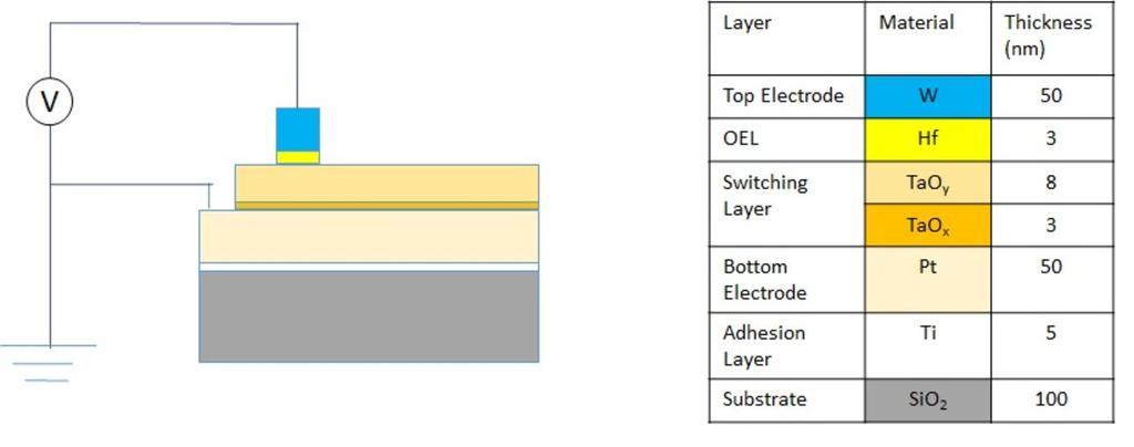
FIG. 1: (a) Schematic of the device showing the material stack and relative thickness of each layer. (b) I-V switching characteristics of the device.
|
|
|
- Amy McDaniel
- 5 years ago
- Views:
Transcription
1 Pulse Width and Height Modulation for Multi-level Resistance in bi-layer TaO x based RRAM Zahiruddin Alamgir, 1 Karsten Beckmann, 1 Joshua Holt, 1 and Nathaniel C. Cady 1 Colleges of Nanoscale Science and Engineering, SUNY Polytechnic Institute, Albany, NY, USA (Dated: 26 July 2017) Mutli-level switching in resistive memory devices enables a wide range of computational paradigms, including neuromorphic and cognitive computing. To this end, we have developed a bilayer tantalum oxide based resistive random access memory (RRAM) device using Hf as the oxygen exchange layer (OEL). Multiple, discrete resistance levels were achieved by modulating RESET pulse width and height, ranging from 2 kω to 142 kω. For a fixed pulse height, OFF state resistance was found to increase gradually with the increase of pulse width whereas for fixed pulse width, increases in pulse height resulted in drastic changes in resistance. Resistive switching in these devices transitioned from Schottky emission in the OFF state to tunneling based conduction in the ON state, based on I-V curve fitting and temperature dependent current measurements. These devices also demonstrated endurance of more than 10 8 cycles with satisfactory Roff/Ron ratio and retention greater than 10 4 s. Keywords: RRAM, MLC, Pulse Width Modulation, Endurance, Retention, Tantalum oxide, Neuromorphic Resistive Random Access Memory (RRAM) devices, which are commonly referred to as memristors, are a strong candidate to replace existing non-volatile memory (NVM) options, such as flash. According to ITRS 2015, Resistive RAM (RRAM) has been categorized as one of the leading emerging memory devices for NVM. RRAM has drawn considerable attention among researchers as a potential candidate for next-generation non-volatile memory, due to its simple structure, fast switching speed 1, endurance, and retention 2. The basic structure of RRAM is a Metal-Insulator-Metal (MIM) structure where single or multi-layers of insulators are sandwiched between two metal electrodes. Besides down-scaling of memory cells, another effective way to increase the memory density is to store more information in a single device. This is commonly referred to as multilevel cell (MLC) storage. For RRAM, multilevel resistive switching has been demonstrated in previous reports by setting the current compliance 3, changing the RESET voltage 4, and modifying the amplitude of the voltage pulse 5 ; however, many of these reports have not shown sufficient endurance of switching within these states, or suffered overlap between the states that can lead to bit read errors. In this study, we demonstrated multilevel resistance states in a W/Hf/TaO y /TaO x /Pt RRAM device by changing the RESET pulse width and height. Hf is placed between the top electrode and the oxide as an oxygen exchange layer (OEL) to scavenge oxygen and (a) (b) FIG. 1: (a) Schematic of the device showing the material stack and relative thickness of each layer. (b) I-V switching characteristics of the device. (a) (b) FIG. 2: (a) Thirteen different resistance levels were reached by changing the RESET pulse Width, while keeping the SET/RESET voltage height and SET pulse width fixed. Each resistance level was maintained for 10 5 consecutive switching pulses. Level one corresponds to ON state resistance. (b) Different resistance levels were also achieved by changing the RESET voltage height and keeping other parameters fixed. thereby modify the stoichiometry of the oxide. As Hf has lower electronegativity (1.23), it can interact more strongly and effectively with oxygen ions nearby the interface, producing high oxygen vacancy concentration at the Hf/TaO x interface and making that interface quasiohmic. Oxygen transfer from the oxide to Hf layer can be explained in terms of thermodynamic driving force (Gibb s free energy). Gibbs free energy for oxide formation of Hf (-1010 kj/mol) is lower than Ti (rutile,-950 kj/mol) or Ta (-760 kj/mol), thus making it more favorable for oxide formation. This high oxygen vacancy concentration at Hf/oxide could facilitate low SET-RESET voltage and resistance uniformity. By changing the pulse width, we were able to modulate resistance gradually, yet each resistance level was distinct and discrete without any overlap. (a) (b) FIG. 3: (a) Average RRAM device resistance state (from Figure 2) were plotted against varying RESET pulse width (a) and RESET pulse height (b).
2 2 (a) (b) FIG. 4: (a) Cumulative distribution of resistance levels for pulse width modulation and (b) cumulative distribution of resistance levels for pulse height modulation. (a) (b) FIG. 5: Switching endurance of RRAM devices was demonstrated for 10 8 cycles is shown in (a), while memory retention at an intermediate resistance level, up to 10 4 s is shown in (b). Beyond memory applications, RRAM also holds promise for use in performing logic functions 6, mimicking neuromorphic activities 7, for use in physically unclonable function (PUF) based hardware encryption 8, or for signal processing 9. One challenge for implementing RRAM for these applications is the significant programming variation in RRAM resistance states, which includes cycle-tocycle variation and stochastic switching, producing unwanted bit flip. In this work, we have demonstrated excellent cycle-to-cycle uniformity for the absolute value of the HRS and LRS resistance states. (a) (b) FIG. 6: (a) I-V plot for RRAM conduction was fit to the Schottky emission equation, with goodness of fit up to 0.73V (marked by red dotted line). (b) Trap assisted tunneling (TAT) plot of I-V data with goodness of fit shown in the higher voltage (V>0.8V) region, shown in the inset. In this study, resistive switching memory (RRAM) devices were fabricated as follows. Pt bottom electrodes with 50 nm thickness were deposited on a Ti/SiO 2 /Si substrate by direct current (DC) sputtering. A 3 nm TaO x film was deposited by radio frequency (RF) magnetron sputtering system (Kurt Lesker PVD sputtering system) in a process gas mixture of Ar and O 2 with flow ratio 3:1, followed by another 8 nm layer of TaO y with Ar and O 2 flow ratio 4:1. The base pressure and the working pressure for the deposition were Torr and Torr, respectively. The deposition of tantalum oxide was carried out at 125 W RF power. Hence, the tantalum oxide layer adjacent to the bottom electrode ( TaO x ) was more stoichiometric than the tantalum oxide layer (TaO y ) on the top of it. As a result, the top oxide layer maintained higher oxygen vacancy concentration and acted as oxygen vacancy reservoir and the lower oxide layer was mainly involved in switching. Finally, a 3 nm oxygen gettering layer of Hf and 50 nm thick top (a) (b) FIG. 7: (a) RRAM device current in the high resistance state (OFF) increased with temperature, following a Schottky emission mechanism. b) Device current was independent of temperature dependence for the low resistance state (ON). electrodes of W were deposited by DC sputtering. These top electrodes were subsequently defined by contact photolithography and a lift-off process. The size of the top electrodes varied from µm 2 to µm 2. An Agilent B1500 semiconductor device analyzer was used to measure the current-voltage characteristics in voltage sweep mode. A transistor was integrated by connecting drain with the bottom electrode (BE) and the source with ground. The top electrode (TE) was biased by applying SET and RESET voltages. The read voltage used for repeat measurements was 0.2 V. The schematic drawing of the device and measurement SET up is shown in Fig. 1(a). Fig. 1(b) shows a typical DC I-V curves of a µm 2 W/Hf/TaO y /TaO x /Pt structure. A soft breakdown (forming step) was achieved usually by applying a voltage higher than SET voltage (5.5 V to 6 V) before the start of device switching. To achieve multilevel pulsebased switching, initially we applied fixed SET voltage with a fixed pulse width (2.6 V/10 µs) to a µm 2 device and gradually varied the RESET pulse width up to 80 µ s, keeping the pulse amplitude fixed -3.3 V. A nondestructive read pulse of 0.2 V was applied after each SET and RESET pulse to measure the resistance of the device. The ON-state resistance level was about 2 kω. The device was cycled in each resistance level for 10 5 times. Thirteen discrete resistance levels were demonstrated, as shown in Fig. 2a. A saturation effect in the OFF state (HRS) was observed as the pulse width was increased, starting at approximately µs. We then increased the pulse height to V, V and V while keeping the pulse width at 80µ s. A drastic increase in resistance occurred in an exponential fashion as we increased the pulse height (Fig. 2(b)). The HRS/LRS ratio increased up to 10 3 as the RESET pulse height was modulated. Fig. 3(a) and 3(b) shows the relationship between pulse width and R off and between Voltages and R off. From these data it can be inferred that the R off can be tuned gradually, by incremental changes to the RESET pulse width. Further, devices exhibited excellent uniformity of resistance at each resistance level (10 5 cycles per level). With such discrete behavior, resistance states can be modulated precisely, making it possible to achieve quasi-analog behavior of the device, which is important for neuromorphic applications 10. No read errors were observed during repeat switching within each level, and no overlap was found between different resistance states. There was almost no cycle-to-cycle variation in the ON state resistance for each level. The cumulative distribution of resistance of different levels achieved by
3 3 modulating pulse width and pulse height are shown in Fig. 4(a) and 4(b), respectively. These data demonstrate that for pulse width modulation, resistance in each level is very uniform. For pulse height base resistance levels, only the 3.38 V RESET voltage yielded high resistance state variability. Excellent endurance was obtained with the devices fabricated in this study, with up to 10 8 switching cycles achieved with pulse-based switching. As can be seen in Fig. 5(a), devices could be switched ON by applying a positive pulse of +2.6 V/20 µs and switched OFF by a negative pulse of 2.8 V/50 µs for the endurance test. The R off /R on ratio was 20:1 throughout these cycles, demonstrating stable performance. The retention properties of the devices are shown in Fig. 3(b). Device were set to HRS and LRS and resistance vs. time was measured with a 0.1 V pulse every 100 s, for each resistance state. The resistance level was maintained for longer than 10 4 s at room temperature, without any noticeable degradation, which indicates good retention properties. To understand the conduction mechanism of these devices, I-V data were plotted (up to the SET point) as Ln ( J/T 2) ) versus E, following the Schottky emission equation and Ln (J) versus 1 / E, following the trap assisted tunneling (TAT) equation. Other conduction mechanism equations such as F-N tunneling, P-F tunneling, etc. were plotted, but did not fit well with measured I-V data. HRS current conduction in the lower voltage region (up to 0.73 V) was found to be dominated by Schottky emission. In the higher voltage regime (>0.8 V), a straight line fit with negative slope in TAT plot indicated that a transition in current conduction from Schottky emission to trap assisted tunneling took place. The extracted barrier height (using the Schottky emission equation) was 0.58 ev while trap height extracted using the TAT equation was about 0.2 ev. We postulate, that as positive bias is applied at the top electrode (negative bias at the bottom electrode), positively charged oxygen vacancies are attracted to the bottom electrode/oxide interface, modulating the Schottky barrier. As oxygen vacancies are effectively donors, the increment of oxygen vacancy concentration at the metal-oxide interface will reduce the Schottky barrier width. This is due to the fact that the width of the Schottky barrier is inversely proportional to the square root of dopant concentration 11. As a result, a transition in current conduction takes place. Additional biasing further causes reduction of the barrier width, and direct tunneling becomes favorable; thus the device switches from HRS to LRS through a transition from Schottky emission to tunneling. To further clarify the switching mechanism, we measured the temperature dependence of device current in both the LRS and HRS. In the HRS, conductance increased with the temperature and a Ln ( I/T 2) vs 1 / T plot exhibited a linear relationship with negative slope (Fig. 7(a)), which further suggests Schottky emission during HRS. In LRS, however, there was almost no discernible change in conductance as temperature was increased (Fig. (7b)), suggesting tunneling based conduction, since this mechanism is generally temperature independent or very weakly temperature dependent 11. We have demonstrated resistance modulation by changing the RESET pulse width with tantalum oxide based RRAM devices. We performed SET-RESET switching for each resistance level for 10 5 times, showing excellent endurance behavior for each level. Several research groups have demonstrated MLC operation in TaO x based RRAM, mostly by changing the peak current compliance during switching 12, or by changing the RESET stop voltage and RESET pulse height 4. Hu et al. has shown multi-level resistance with TaO x based RRAM through controlling different RESET stop voltages and different compliance currents in direct current voltage sweeping modes and by means of different pulse erasing voltages in pulse programming/erasing modes 13. In many cases, individual resistance levels were not switched for a sufficient number of cycles, and many of the resistance states exhibited large variation. In this study, when using bi-layer TaO x based RRAM with Hf as the OEL, each resistance level was uniform and non-overlapping, and hence, is suitable for applications where cycle to cycle uniformity is of utmost importance. We propose two possible reasons for this uniformity. First, the µs timescale for pulse application could be helpful for achieving stable and uniform resistance levels. In particular, we observed that shorter RESET pulse widths were associated with reduced resistance variability (Fig. (2a), Fig. (4a)). Second, the Hf OEL and sub-stoichiometric TaO y layer may have led to a higher concentration of oxygen vacancies, that in turn, could induce higher vacancy movement and facilitate more uniform resistance levels. For oxygen vacancy concentrations greater than a certain level, the local lattice becomes distorted and strained, leading to a greatly increased diffusion constant for oxygen vacancy 14. These devices also show good endurance and retention and high R off /R on ratio for longer cycles. For a fixed RESET pulse height, change in pulse width caused a gradual change in the resistance level. When the pulse height was changed keeping the pulse width fixed, however, caused a drastic change in R off. These results demonstrate multilevel storage capability and suggest that our devices are amenable to applications such as neuromorphic computing and hardware based encryption system. Finally, based on the electrical measurement results, curve fitting, and temperature based study, we suggest that Schottky emission dominates at the HRS, while trap assisted tunneling dominates at higher voltages, and the device switches from HRS to LRS through a transition from Schottky emission to tunneling. ACKNOWLEDGMENTS The authors would like to thank the Air Force Research Laboratory for financial support under contract FA (PI Nathaniel Cady). 1 A. C. Torrezan, J. P. Strachan, G. Medeiros-Ribeiro, and R. S. Williams, Nanotechnology 22, (2011). 2 Z. Wei, S. Kanzawa, Y Mitani, and S. Fujii, in Electron Devices Meeting, IEDM IEEE International (IEEE, 2008) pp M.-C. Wu, W.-Y. Jang, C.-H. Lin, and T.-Y. Tseng, Semiconductor Science and Technology 27, (2012).
4 4 4 W. Kim, S. Menzel, D. Wouters, R. Waser, and V. Rana, IEEE Electron Device Letters 37, 564 (2016). 5 L. Zhao, H.-Y. Chen, S.-C. Wu, Z. Jiang, S. Yu, T.-H. Hou, H.-S. Philip Wong, and Y. Nishi, Nanoscale 6, 5698 (2014). 6 Z. Alamgir, K. Beckmann, N. Cady, A. Velasquez, and S. K. Jha, in Circuits and Systems (ISCAS), 2016 IEEE International Symposium on (IEEE, 2016) pp K.-H. Kim, S. Gaba, D. Wheeler, J. M. Cruz-Albrecht, T. Hussain, N. Srinivasa, and W. Lu, Nano letters 12, 389 (2011). 8 G. S. Rose, N. McDonald, L.-K. Yan, and B. Wysocki, in Proceedings of the International Conference on Computer-Aided Design (IEEE Press, 2013) pp X. Hu, S. Duan, L. Wang, and X. Liao, Science China Information Sciences 55, 461 (2012). 10 Y. Wu, S. Yu, H.-S. P. Wong, Y.-S. Chen, H.-Y. Lee, S.-M. Wang, P.-Y. Gu, F. Chen, and M.-J. Tsai, in Memory Workshop (IMW), th IEEE International (IEEE, 2012) pp N. K. K. Sze Simon M., Physics of Semiconductor Devices (Wiley, 2007). 12 A. Prakash, J. Park, J. Song, J. Woo, E.-J. Cha, and H. Hwang, IEEE Electron Device Letters 36, 32 (2015). 13 W. Hu, L. Zou, C. Gao, Y. Guo, and D. Bao, Journal of Alloys and Compounds 676, 356 (2016). 14 Y. Nian, J. Strozier, N. Wu, X. Chen, and A. Ignatiev, Physical review letters 98, (2007).
5
6 Current ( µa) Reset State Set State Set State Reset State Set Point Reset Point Voltage (V)
7
8 Resistance (kω) V V V 2 Cycle Number x 10
9 150 Resistance (kω) Pulse Width (µs)
10 5000 Resistance (kω) Voltages(V)
11 (µs) 1 Cumulative Probability (F(x)) Resistance (kω)
12 1 Cumulative Probability (F(x)) V 3.33 V 3.3 V 3.38 V Resistance (kω)
13 10 5 Roff Ron Resistance (Ω) Cycle Number
14 10 6 Resistance (Ω) Roff Ron Time (sec)
15 Ln (Js/T 2 ) Barrier Height = 0.58 ev Schottky Emission Mechanism Data Linear fitting E (V/cm)
16 Ln (J) Trap Assisted Tunneling Plot x E 1 (m/v) x 10 7
17 Ln (I/T 2 ) HRS /T (K 1)
18 400 Current (µ A) LRS Temperature (K)
HfO 2 Based Resistive Switching Non-Volatile Memory (RRAM) and Its Potential for Embedded Applications
 and Its Potential for Embedded Applications") 2012 International Conference on Solid-State and Integrated Circuit (ICSIC 2012) IPCSIT vol. 32 (2012) (2012) IACSIT Press, Singapore HfO 2 Based Resistive Switching Non-Volatile Memory (RRAM) and Its
2012 International Conference on Solid-State and Integrated Circuit (ICSIC 2012) IPCSIT vol. 32 (2012) (2012) IACSIT Press, Singapore HfO 2 Based Resistive Switching Non-Volatile Memory (RRAM) and Its
Analog Synaptic Behavior of a Silicon Nitride Memristor
 Supporting Information Analog Synaptic Behavior of a Silicon Nitride Memristor Sungjun Kim, *, Hyungjin Kim, Sungmin Hwang, Min-Hwi Kim, Yao-Feng Chang,, and Byung-Gook Park *, Inter-university Semiconductor
3D Vertical Dual-Layer Oxide Memristive Devices for Neuromorphic Computing
 3D Vertical Dual-Layer Oxide Memristive Devices for Neuromorphic Computing Siddharth Gaba, Patrick Sheridan, Chao Du, and Wei Lu* Electrical Engineering and Computer Science, University of Michigan, Ann
In-Line-Test of Variability and Bit-Error-Rate of HfO x -Based Resistive Memory
 This manuscript is the accepted version of the following IEEE conference paper: Ji, B.L.; Li, H.; Ye, Q.; Gausepohl, S.; Deora, S.; Veksler, D.; Vivekanand, S.; Chong, H.; Stamper, H.; Burroughs, T.; Johnson,
Supplementary Information. implantation of bottom electrodes
 Supplementary Information Engineering interface-type resistive switching in BiFeO3 thin film switches by Ti implantation of bottom electrodes Tiangui You, 1,2 Xin Ou, 1,* Gang Niu, 3 Florian Bärwolf, 3
Conductance switching in Ag 2 S devices fabricated by sulphurization
 3 Conductance switching in Ag S devices fabricated by sulphurization The electrical characterization and switching properties of the α-ag S thin films fabricated by sulfurization are presented in this
Atomristor: Non-Volatile Resistance Switching in Atomic Sheets of
 Atomristor: Non-Volatile Resistance Switching in Atomic Sheets of Transition Metal Dichalcogenides Ruijing Ge 1, Xiaohan Wu 1, Myungsoo Kim 1, Jianping Shi 2, Sushant Sonde 3,4, Li Tao 5,1, Yanfeng Zhang
Supplementary Figure 1 Schematic illustration of fabrication procedure of MoS2/h- BN/graphene heterostructures. a, c d Supplementary Figure 2
 Supplementary Figure 1 Schematic illustration of fabrication procedure of MoS 2 /hon a 300- BN/graphene heterostructures. a, CVD-grown b, Graphene was patterned into graphene strips by oxygen monolayer
Supplementary Figures
 Supplementary Figures Supplementary Figure 1. The schematic of the perceptron. Here m is the index of a pixel of an input pattern and can be defined from 1 to 320, j represents the number of the output
Future MOSFET Devices using high-k (TiO 2 ) dielectric
 dielectric") Future MOSFET Devices using high-k (TiO 2 ) dielectric Prerna Guru Jambheshwar University, G.J.U.S. & T., Hisar, Haryana, India, prernaa.29@gmail.com Abstract: In this paper, an 80nm NMOS with high-k (TiO
Future MOSFET Devices using high-k (TiO 2 ) dielectric Prerna Guru Jambheshwar University, G.J.U.S. & T., Hisar, Haryana, India, prernaa.29@gmail.com Abstract: In this paper, an 80nm NMOS with high-k (TiO
CMOS Analog Integrate-and-fire Neuron Circuit for Driving Memristor based on RRAM
 JOURNAL OF SEMICONDUCTOR TECHNOLOGY AND SCIENCE, VOL.17, NO.2, APRIL, 2017 ISSN(Print) 1598-1657 https://doi.org/10.5573/jsts.2017.17.2.174 ISSN(Online) 2233-4866 CMOS Analog Integrate-and-fire Neuron
Supporting Information. Vertical Graphene-Base Hot-Electron Transistor
 Supporting Information Vertical Graphene-Base Hot-Electron Transistor Caifu Zeng, Emil B. Song, Minsheng Wang, Sejoon Lee, Carlos M. Torres Jr., Jianshi Tang, Bruce H. Weiller, and Kang L. Wang Department
I-V Characteristics of Al/HfO2/TaN RRAM Devices
 I-V Characteristics of Al/HfO2/TaN RRAM Devices By Arturo H. Valdivia A Project submitted to Oregon State University Honors College in partial fulfillment of the requirements for the degree of Honors Baccalaureate
Power MOSFET Zheng Yang (ERF 3017,
 ECE442 Power Semiconductor Devices and Integrated Circuits Power MOSFET Zheng Yang (ERF 3017, email: yangzhen@uic.edu) Evolution of low-voltage (
Department of Electrical Engineering IIT Madras
 Department of Electrical Engineering IIT Madras Sample Questions on Semiconductor Devices EE3 applicants who are interested to pursue their research in microelectronics devices area (fabrication and/or
CHAPTER 3 TWO DIMENSIONAL ANALYTICAL MODELING FOR THRESHOLD VOLTAGE
 49 CHAPTER 3 TWO DIMENSIONAL ANALYTICAL MODELING FOR THRESHOLD VOLTAGE 3.1 INTRODUCTION A qualitative notion of threshold voltage V th is the gate-source voltage at which an inversion channel forms, which
Non-Volatile Memory Based on Solid Electrolytes
 Non-Volatile Memory Based on Solid Electrolytes Michael Kozicki Chakku Gopalan Murali Balakrishnan Mira Park Maria Mitkova Center for Solid State Electronics Research Introduction The electrochemical redistribution
Fabrication and Characterization of Emerging Nanoscale Memory
 Fabrication and Characterization of Emerging Nanoscale Memory Yuan Zhang, SangBum Kim, Byoungil Lee, Marissa Caldwell(*), and (*) Chemistry Department Stanford University, Stanford, California, U.S.A.
Supporting Information. Air-stable surface charge transfer doping of MoS 2 by benzyl viologen
 Supporting Information Air-stable surface charge transfer doping of MoS 2 by benzyl viologen Daisuke Kiriya,,ǁ, Mahmut Tosun,,ǁ, Peida Zhao,,ǁ, Jeong Seuk Kang, and Ali Javey,,ǁ,* Electrical Engineering
CHAPTER 9 CURRENT VOLTAGE CHARACTERISTICS
 CHAPTER 9 CURRENT VOLTAGE CHARACTERISTICS 9.1 INTRODUCTION The phthalocyanines are a class of organic materials which are generally thermally stable and may be deposited as thin films by vacuum evaporation
RRAM based analog synapse device for neuromorphic system
 RRAM based analog synapse device for neuromorphic system Kibong Moon, Euijun Cha, and Hyunsang Hwang Pohang University of Science and Technology (POSTECH), Korea The 13 th Korea-U.S. Forum on Nanotechnology,
Atomic-layer deposition of ultrathin gate dielectrics and Si new functional devices
 Atomic-layer deposition of ultrathin gate dielectrics and Si new functional devices Anri Nakajima Research Center for Nanodevices and Systems, Hiroshima University 1-4-2 Kagamiyama, Higashi-Hiroshima,
Design and Analysis of Double Gate MOSFET Devices using High-k Dielectric
 International Journal of Electrical Engineering. ISSN 0974-2158 Volume 7, Number 1 (2014), pp. 53-60 International Research Publication House http://www.irphouse.com Design and Analysis of Double Gate
In pursuit of high-density storage class memory
 Edition October 2017 Semiconductor technology & processing In pursuit of high-density storage class memory A novel thermally stable GeSe-based selector paves the way to storage class memory applications.
Self-compliance RRAM characteristics using a novel W/TaO x /TiN structure
 Maikap et al. Nanoscale Research Letters 2014, 9:292 NANO EXPRESS Self-compliance RRAM characteristics using a novel W/TaO x /TiN structure Siddheswar Maikap *, Debanjan Jana, Mrinmoy Dutta and Amit Prakash
64 Kb logic RRAM chip resisting physical and side-channel attacks for encryption keys storage
 64 Kb logic RRAM chip resisting physical and side-channel attacks for encryption keys storage Yufeng Xie a), Wenxiang Jian, Xiaoyong Xue, Gang Jin, and Yinyin Lin b) ASIC&System State Key Lab, Dept. of
Supporting Information. Single-Nanowire Electrochemical Probe Detection for Internally Optimized Mechanism of
 Supporting Information Single-Nanowire Electrochemical Probe Detection for Internally Optimized Mechanism of Porous Graphene in Electrochemical Devices Ping Hu, Mengyu Yan, Xuanpeng Wang, Chunhua Han,*
Review Energy Bands Carrier Density & Mobility Carrier Transport Generation and Recombination
 Review Energy Bands Carrier Density & Mobility Carrier Transport Generation and Recombination Current Transport: Diffusion, Thermionic Emission & Tunneling For Diffusion current, the depletion layer is
Parameter Optimization Of GAA Nano Wire FET Using Taguchi Method
 Parameter Optimization Of GAA Nano Wire FET Using Taguchi Method S.P. Venu Madhava Rao E.V.L.N Rangacharyulu K.Lal Kishore Professor, SNIST Professor, PSMCET Registrar, JNTUH Abstract As the process technology
Lecture #29. Moore s Law
 Lecture #29 ANNOUNCEMENTS HW#15 will be for extra credit Quiz #6 (Thursday 5/8) will include MOSFET C-V No late Projects will be accepted after Thursday 5/8 The last Coffee Hour will be held this Thursday
Design of Enhancement Mode Single-gate and Double-gate Multi-channel GaN HEMT with Vertical Polarity Inversion Heterostructure
 MITSUBISHI ELECTRIC RESEARCH LABORATORIES http://www.merl.com Design of Enhancement Mode Single-gate and Double-gate Multi-channel GaN HEMT with Vertical Polarity Inversion Heterostructure Feng, P.; Teo,
Depletion width measurement in an organic Schottky contact using a Metal-
 Depletion width measurement in an organic Schottky contact using a Metal- Semiconductor Field-Effect Transistor Arash Takshi, Alexandros Dimopoulos and John D. Madden Department of Electrical and Computer
2014, IJARCSSE All Rights Reserved Page 1352
 Volume 4, Issue 3, March 2014 ISSN: 2277 128X International Journal of Advanced Research in Computer Science and Software Engineering Research Paper Available online at: www.ijarcsse.com Double Gate N-MOSFET
Body-Biased Complementary Logic Implemented Using AlN Piezoelectric MEMS Switches
 University of Pennsylvania From the SelectedWorks of Nipun Sinha 29 Body-Biased Complementary Logic Implemented Using AlN Piezoelectric MEMS Switches Nipun Sinha, University of Pennsylvania Timothy S.
SUPPLEMENTARY INFORMATION
 SUPPLEMENTARY INFORMATION Dopant profiling and surface analysis of silicon nanowires using capacitance-voltage measurements Erik C. Garnett 1, Yu-Chih Tseng 4, Devesh Khanal 2,3, Junqiao Wu 2,3, Jeffrey
Resistive Switching Memory in Integration
 EDS Mini Colloquim WIMNACT 39, Tokyo Resistive Switching Memory in Integration Ming Liu Institute of Microelectronics, CAS Feb.7, 2014 Outline Motivation RRAM Integration Self-Rectifying RRAM 1D1R Integration
SUPPLEMENTARY INFORMATION
 A fast, high endurance and scalable non-volatile memory device made from asymmetric Ta 2 O 5-x /TaO 2-x bilayer structures Myoung-Jae Lee 1, Chang Bum Lee 1, Dongsoo Lee 1, Seung Ryul Lee 1, Man Chang
3. COMPARING STRUCTURE OF SINGLE GATE AND DOUBLE GATE MOSFET WITH DESIGN AND CURVE
 P a g e 80 Available online at http://arjournal.org APPLIED RESEARCH JOURNAL RESEARCH ARTICLE ISSN: 2423-4796 Applied Research Journal Vol. 3, Issue, 2, pp.80-86, February, 2017 COMPARATIVE STUDY ON SINGLE
INVESTIGATION OF RESISTIVE SWITCHING AND CONDUCTION MECHANISMS IN OXIDE-BASED RRAM DEVICE FOR EMERGING NONVOLATILE MEMORY APPLICATIONS
 INVESTIGATION OF RESISTIVE SWITCHING AND CONDUCTION MECHANISMS IN OXIDE-BASED RRAM DEVICE FOR EMERGING NONVOLATILE MEMORY APPLICATIONS FANG ZHENG SCHOOL OF ELECTRICAL & ELECTRONIC ENGINEERING NANYANG TECHNOLOGICAL
Influence of Fin Shape and Temperature on Conventional and Strained MuGFETs Analog Parameters
 02 (49)-AF:Modelo-AF 8/20/11 6:25 AM Page 94 Influence of Fin Shape and Temperature on Conventional and Strained MuGFETs Analog Parameters Rudolf Theoderich Bühler 1, Renato Giacomini 1,2 and João Antonio
SiGe epitaxial memory for neuromorphic computing with reproducible high performance based on engineered dislocations
 SUPPLEMENTARY INFORMATION Articles https://doi.org/10.1038/s41563-017-0001-5 In the format provided by the authors and unedited. SiGe epitaxial memory for neuromorphic computing with reproducible high
Supplementary Materials for
 advances.sciencemag.org/cgi/content/full/2/6/e1501326/dc1 Supplementary Materials for Organic core-sheath nanowire artificial synapses with femtojoule energy consumption Wentao Xu, Sung-Yong Min, Hyunsang
Solid State Device Fundamentals
 Solid State Device Fundamentals 4.4. Field Effect Transistor (MOSFET) ENS 463 Lecture Course by Alexander M. Zaitsev alexander.zaitsev@csi.cuny.edu Tel: 718 982 2812 4N101b 1 Field-effect transistor (FET)
A scanning tunneling microscopy based potentiometry technique and its application to the local sensing of the spin Hall effect
 A scanning tunneling microscopy based potentiometry technique and its application to the local sensing of the spin Hall effect Ting Xie 1, a), Michael Dreyer 2, David Bowen 3, Dan Hinkel 3, R. E. Butera
Binary Neural Network and Its Implementation with 16 Mb RRAM Macro Chip
 Binary Neural Network and Its Implementation with 16 Mb RRAM Macro Chip Assistant Professor of Electrical Engineering and Computer Engineering shimengy@asu.edu http://faculty.engineering.asu.edu/shimengyu/
Design and Implementation of less quiescent current, less dropout LDO Regulator in 90nm Technology Madhukumar A S #1, M.
 Design and Implementation of less quiescent current, less dropout LDO Regulator in 90nm Technology Madhukumar A S #1, M.Nagabhushan #2 #1 M.Tech student, Dept. of ECE. M.S.R.I.T, Bangalore, INDIA #2 Asst.
Supplementary Information
 Supplementary Information Wireless thin film transistor based on micro magnetic induction coupling antenna Byoung Ok Jun 1, Gwang Jun Lee 1, Jong Gu Kang 1,2, Seung Uk Kim 1, Ji Woong Choi 1, Seung Nam
Improved switching characteristics of TiO 2-x ReRAM with embedded ultra-thin Al 2 O 3-y layers
 1 2 3 4 5 6 Improved switching characteristics of TiO 2-x ReRAM with embedded ultra-thin Al 2 O 3-y layers Maria Trapatseli, Simone Cortese, Alexantrou Serb, and Themistoklis Prodromakis Nano Group, School
Gallium nitride (GaN)
") 80 Technology focus: GaN power electronics Vertical, CMOS and dual-gate approaches to gallium nitride power electronics US research company HRL Laboratories has published a number of papers concerning
80 Technology focus: GaN power electronics Vertical, CMOS and dual-gate approaches to gallium nitride power electronics US research company HRL Laboratories has published a number of papers concerning
Lecture-45. MOS Field-Effect-Transistors Threshold voltage
 Lecture-45 MOS Field-Effect-Transistors 7.4. Threshold voltage In this section we summarize the calculation of the threshold voltage and discuss the dependence of the threshold voltage on the bias applied
Journal of Electron Devices, Vol. 20, 2014, pp
 Journal of Electron Devices, Vol. 20, 2014, pp. 1786-1791 JED [ISSN: 1682-3427 ] ANALYSIS OF GIDL AND IMPACT IONIZATION WRITING METHODS IN 100nm SOI Z-DRAM Bhuwan Chandra Joshi, S. Intekhab Amin and R.
Performance Comparison of CMOS and Finfet Based Circuits At 45nm Technology Using SPICE
 RESEARCH ARTICLE OPEN ACCESS Performance Comparison of CMOS and Finfet Based Circuits At 45nm Technology Using SPICE Mugdha Sathe*, Dr. Nisha Sarwade** *(Department of Electrical Engineering, VJTI, Mumbai-19)
Dependence of Carbon Nanotube Field Effect Transistors Performance on Doping Level of Channel at Different Diameters: on/off current ratio
 Copyright (2012) American Institute of Physics. This article may be downloaded for personal use only. Any other use requires prior permission of the author and the American Institute of Physics. The following
Sub-Threshold Region Behavior of Long Channel MOSFET
 Sub-threshold Region - So far, we have discussed the MOSFET behavior in linear region and saturation region - Sub-threshold region is refer to region where Vt is less than Vt - Sub-threshold region reflects
Resistive Switching Mechanisms on TaO x and SrRuO 3 Thin Film Surfaces Probed by Scanning Tunneling Microscopy
 Resistive Switching Mechanisms on TaO x and SrRuO 3 Thin Film Surfaces Probed by Scanning Tunneling Microscopy Marco Moors, 1# Kiran Kumar Adepalli, 2,3# Qiyang Lu, 3 Anja Wedig, 1 Christoph Bäumer, 1
Chapter 1. Introduction
 Chapter 1 Introduction 1.1 Introduction of Device Technology Digital wireless communication system has become more and more popular in recent years due to its capability for both voice and data communication.
Experiment 3. 3 MOSFET Drain Current Modeling. 3.1 Summary. 3.2 Theory. ELEC 3908 Experiment 3 Student#:
 Experiment 3 3 MOSFET Drain Current Modeling 3.1 Summary In this experiment I D vs. V DS and I D vs. V GS characteristics are measured for a silicon MOSFET, and are used to determine the parameters necessary
Contribution of Gate Induced Drain Leakage to Overall Leakage and Yield Loss in Digital submicron VLSI Circuits
 Contribution of Gate Induced Drain Leakage to Overall Leakage and Yield Loss in Digital submicron VLSI Circuits Oleg Semenov, Andrzej Pradzynski * and Manoj Sachdev Dept. of Electrical and Computer Engineering,
MSE 410/ECE 340: Electrical Properties of Materials Fall 2016 Micron School of Materials Science and Engineering Boise State University
 MSE 410/ECE 340: Electrical Properties of Materials Fall 2016 Micron School of Materials Science and Engineering Boise State University Practice Final Exam 1 Read the questions carefully Label all figures
Low-field behaviour of source-gated transistors
 Low-field behaviour of source-gated transistors J. M. Shannon, R. A. Sporea*, Member, IEEE, S. Georgakopoulos, M. Shkunov, Member, IEEE, and S. R. P. Silva Manuscript received February 5, 2013. The work
DESIGN OF AN S-BAND TWO-WAY INVERTED ASYM- METRICAL DOHERTY POWER AMPLIFIER FOR LONG TERM EVOLUTION APPLICATIONS
 Progress In Electromagnetics Research Letters, Vol. 39, 73 80, 2013 DESIGN OF AN S-BAND TWO-WAY INVERTED ASYM- METRICAL DOHERTY POWER AMPLIFIER FOR LONG TERM EVOLUTION APPLICATIONS Hai-Jin Zhou * and Hua
NAME: Last First Signature
 UNIVERSITY OF CALIFORNIA, BERKELEY College of Engineering Department of Electrical Engineering and Computer Sciences EE 130: IC Devices Spring 2003 FINAL EXAMINATION NAME: Last First Signature STUDENT
Transparent p-type SnO Nanowires with Unprecedented Hole Mobility among Oxide Semiconductors
 Supplementary Information Transparent p-type SnO Nanowires with Unprecedented Hole Mobility among Oxide Semiconductors J. A. Caraveo-Frescas and H. N. Alshareef* Materials Science and Engineering, King
Vertical Nanowall Array Covered Silicon Solar Cells
 International Conference on Solid-State and Integrated Circuit (ICSIC ) IPCSIT vol. () () IACSIT Press, Singapore Vertical Nanowall Array Covered Silicon Solar Cells J. Wang, N. Singh, G. Q. Lo, and D.
Charge-Based Continuous Equations for the Transconductance and Output Conductance of Graded-Channel SOI MOSFET s
 Charge-Based Continuous Equations for the Transconductance and Output Conductance of Graded-Channel SOI MOSFET s Michelly de Souza 1 and Marcelo Antonio Pavanello 1,2 1 Laboratório de Sistemas Integráveis,
Chapter 6. Silicon-Germanium Technologies
 Chapter 6 licon-germanium Technologies 6.0 Introduction The design of bipolar transistors requires trade-offs between a number of parameters. To achieve a fast base transit time, hence achieving a high
Design of Dynamic Frequency Divider using Negative Differential Resistance Circuit
 Design of Dynamic Frequency Divider using Negative Differential Resistance Circuit Kwang-Jow Gan 1*, Kuan-Yu Chun 2, Wen-Kuan Yeh 3, Yaw-Hwang Chen 2, and Wein-So Wang 2 1 Department of Electrical Engineering,
Semiconductor Memory: DRAM and SRAM. Department of Electrical and Computer Engineering, National University of Singapore
 Semiconductor Memory: DRAM and SRAM Outline Introduction Random Access Memory (RAM) DRAM SRAM Non-volatile memory UV EPROM EEPROM Flash memory SONOS memory QD memory Introduction Slow memories Magnetic
EFFECT OF THRESHOLD VOLTAGE AND CHANNEL LENGTH ON DRAIN CURRENT OF SILICON N-MOSFET
 EFFECT OF THRESHOLD VOLTAGE AND CHANNEL LENGTH ON DRAIN CURRENT OF SILICON N-MOSFET A.S.M. Bakibillah Nazibur Rahman Dept. of Electrical & Electronic Engineering, American International University Bangladesh
ECSE-6300 IC Fabrication Laboratory Lecture 9 MOSFETs. Lecture Outline
 ECSE-6300 IC Fabrication Laboratory Lecture 9 MOSFETs Prof. Rensselaer Polytechnic Institute Troy, NY 12180 Office: CII-6229 Tel.: (518) 276-2909 e-mails: luj@rpi.edu http://www.ecse.rpi.edu/courses/s18/ecse
Variation-Aware Design for Nanometer Generation LSI
 HIRATA Morihisa, SHIMIZU Takashi, YAMADA Kenta Abstract Advancement in the microfabrication of semiconductor chips has made the variations and layout-dependent fluctuations of transistor characteristics
Low Power Design of Successive Approximation Registers
 Low Power Design of Successive Approximation Registers Rabeeh Majidi ECE Department, Worcester Polytechnic Institute, Worcester MA USA rabeehm@ece.wpi.edu Abstract: This paper presents low power design
MOSFET short channel effects
 MOSFET short channel effects overview Five different short channel effects can be distinguished: velocity saturation drain induced barrier lowering (DIBL) impact ionization surface scattering hot electrons
improving further the mobility, and therefore the channel conductivity. The positive pattern definition proposed by Hirayama [6] was much improved in
![improving further the mobility, and therefore the channel conductivity. The positive pattern definition proposed by Hirayama [6] was much improved in](/thumbs/91/107553446.jpg "improving further the mobility, and therefore the channel conductivity. The positive pattern definition proposed by Hirayama [6] was much improved in") The two-dimensional systems embedded in modulation-doped heterostructures are a very interesting and actual research field. The FIB implantation technique can be successfully used to fabricate using these
The two-dimensional systems embedded in modulation-doped heterostructures are a very interesting and actual research field. The FIB implantation technique can be successfully used to fabricate using these
Author(s) Osamu; Nakamura, Tatsuya; Katagiri,
 Osamu; Nakamura, Tatsuya; Katagiri,") TitleCryogenic InSb detector for radiati Author(s) Kanno, Ikuo; Yoshihara, Fumiki; Nou Osamu; Nakamura, Tatsuya; Katagiri, Citation REVIEW OF SCIENTIFIC INSTRUMENTS (2 2533-2536 Issue Date 2002-07 URL
TitleCryogenic InSb detector for radiati Author(s) Kanno, Ikuo; Yoshihara, Fumiki; Nou Osamu; Nakamura, Tatsuya; Katagiri, Citation REVIEW OF SCIENTIFIC INSTRUMENTS (2 2533-2536 Issue Date 2002-07 URL
Supplementary Information
 Normalized Intensity Current (A) Supplementary Information 10-2 10-3 10-4 10-5 10-6 10-7 10-8 10-9 30x30 m 2 V set V reset Electroforming Pt/ / /Pt 10-10 -4-3 -2-1 0 1 2 3 4 5 Voltage (V) Pt/ / /SiO 2
3D SOI elements for System-on-Chip applications
 Advanced Materials Research Online: 2011-07-04 ISSN: 1662-8985, Vol. 276, pp 137-144 doi:10.4028/www.scientific.net/amr.276.137 2011 Trans Tech Publications, Switzerland 3D SOI elements for System-on-Chip
7. Bipolar Junction Transistor
 41 7. Bipolar Junction Transistor 7.1. Objectives - To experimentally examine the principles of operation of bipolar junction transistor (BJT); - To measure basic characteristics of n-p-n silicon transistor
Broadband analog phase shifter based on multi-stage all-pass networks
 This article has been accepted and published on J-STAGE in advance of copyediting. Content is final as presented. IEICE Electronics Express, Vol.* No.*,*-* Broadband analog phase shifter based on multi-stage
Solid State Devices- Part- II. Module- IV
 Solid State Devices- Part- II Module- IV MOS Capacitor Two terminal MOS device MOS = Metal- Oxide- Semiconductor MOS capacitor - the heart of the MOSFET The MOS capacitor is used to induce charge at the
Design & Performance Analysis of DG-MOSFET for Reduction of Short Channel Effect over Bulk MOSFET at 20nm
 RESEARCH ARTICLE OPEN ACCESS Design & Performance Analysis of DG- for Reduction of Short Channel Effect over Bulk at 20nm Ankita Wagadre*, Shashank Mane** *(Research scholar, Department of Electronics
EXPERIMENT 10: SCHOTTKY DIODE CHARACTERISTICS
 EXPERIMENT 10: SCHOTTKY DIODE CHARACTERISTICS AIM: To plot forward and reverse characteristics of Schottky diode (Metal Semiconductor junction) APPARATUS: D.C. Supply (0 15 V), current limiting resistor
Laboratory #5 BJT Basics and MOSFET Basics
 Laboratory #5 BJT Basics and MOSFET Basics I. Objectives 1. Understand the physical structure of BJTs and MOSFETs. 2. Learn to measure I-V characteristics of BJTs and MOSFETs. II. Components and Instruments
Open Access. C.H. Ho 1, F.T. Chien 2, C.N. Liao 1 and Y.T. Tsai*,1
 56 The Open Electrical and Electronic Engineering Journal, 2008, 2, 56-61 Open Access Optimum Design for Eliminating Back Gate Bias Effect of Silicon-oninsulator Lateral Double Diffused Metal-oxide-semiconductor
E LECTROOPTICAL(EO)modulatorsarekeydevicesinoptical
modulatorsarekeydevicesinoptical") 286 JOURNAL OF LIGHTWAVE TECHNOLOGY, VOL. 26, NO. 2, JANUARY 15, 2008 Design and Fabrication of Sidewalls-Extended Electrode Configuration for Ridged Lithium Niobate Electrooptical Modulator Yi-Kuei Wu,
286 JOURNAL OF LIGHTWAVE TECHNOLOGY, VOL. 26, NO. 2, JANUARY 15, 2008 Design and Fabrication of Sidewalls-Extended Electrode Configuration for Ridged Lithium Niobate Electrooptical Modulator Yi-Kuei Wu,
Performance Analysis of 20 nm Pentagonal and Trapezoidal NanoWire Transistor with Si and Ge Channel
 Performance Analysis of 20 nm Pentagonal and Trapezoidal NanoWire Transistor with Si and Ge Channel SANDEEP SINGH GILL 1, JAIDEV KAUSHIK 2, NAVNEET KAUR 3 Department of Electronics and Communication Engineering
CHAPTER 2 LITERATURE REVIEW
 CHAPTER 2 LITERATURE REVIEW 2.1 Introduction of MOSFET The structure of the MOS field-effect transistor (MOSFET) has two regions of doping opposite that of the substrate, one at each edge of the MOS structure
Effect of Channel Doping Concentration on the Impact ionization of n- Channel Fully Depleted SOI MOSFET
 International Journal of Engineering Works Kambohwell Publisher Enterprises Vol. 2, Issue 2, PP. 18-22, Feb. 2015 www.kwpublisher.com Effect of Channel Doping Concentration on the Impact ionization of
SRM INSTITUTE OF SCIENCE AND TECHNOLOGY (DEEMED UNIVERSITY)
") SRM INSTITUTE OF SCIENCE AND TECHNOLOGY (DEEMED UNIVERSITY) QUESTION BANK I YEAR B.Tech (II Semester) ELECTRONIC DEVICES (COMMON FOR EC102, EE104, IC108, BM106) UNIT-I PART-A 1. What are intrinsic and
SRM INSTITUTE OF SCIENCE AND TECHNOLOGY (DEEMED UNIVERSITY) QUESTION BANK I YEAR B.Tech (II Semester) ELECTRONIC DEVICES (COMMON FOR EC102, EE104, IC108, BM106) UNIT-I PART-A 1. What are intrinsic and
Fabrication and electrical characterization of MONOS memory with novel high-κ gate stack
 Title Fabrication and electrical characterization of MONOS memory with novel high-κ gate stack Author(s) Liu, L; Xu, JP; Chan, CL; Lai, PT Citation The IEEE International Conference on Electron Devices
IMPROVED CURRENT MIRROR OUTPUT PERFORMANCE BY USING GRADED-CHANNEL SOI NMOSFETS
 IMPROVED CURRENT MIRROR OUTPUT PERFORMANCE BY USING GRADED-CHANNEL SOI NMOSFETS Marcelo Antonio Pavanello *, João Antonio Martino and Denis Flandre 1 Laboratório de Sistemas Integráveis Escola Politécnica
A new Hetero-material Stepped Gate (HSG) SOI LDMOS for RF Power Amplifier Applications
 SOI LDMOS for RF Power Amplifier Applications") A new Hetero-material Stepped Gate (HSG) SOI LDMOS for RF Power Amplifier Applications Radhakrishnan Sithanandam and M. Jagadesh Kumar, Senior Member, IEEE Department of Electrical Engineering Indian Institute
A new Hetero-material Stepped Gate (HSG) SOI LDMOS for RF Power Amplifier Applications Radhakrishnan Sithanandam and M. Jagadesh Kumar, Senior Member, IEEE Department of Electrical Engineering Indian Institute
semiconductor p-n junction Potential difference across the depletion region is called the built-in potential barrier, or built-in voltage:
 Chapter four The Equilibrium pn Junction The Electric field will create a force that will stop the diffusion of carriers reaches thermal equilibrium condition Potential difference across the depletion
Session 10: Solid State Physics MOSFET
 Session 10: Solid State Physics MOSFET 1 Outline A B C D E F G H I J 2 MOSCap MOSFET Metal-Oxide-Semiconductor Field-Effect Transistor: Al (metal) SiO2 (oxide) High k ~0.1 ~5 A SiO2 A n+ n+ p-type Si (bulk)
Enhanced Emitter Transit Time for Heterojunction Bipolar Transistors (HBT)
") Advances in Electrical Engineering Systems (AEES)` 196 Vol. 1, No. 4, 2013, ISSN 2167-633X Copyright World Science Publisher, United States www.worldsciencepublisher.org Enhanced Emitter Transit Time for
Advances in Electrical Engineering Systems (AEES)` 196 Vol. 1, No. 4, 2013, ISSN 2167-633X Copyright World Science Publisher, United States www.worldsciencepublisher.org Enhanced Emitter Transit Time for
Substrate effect on the resistive switching in BiFeO 3 thin films
 Substrate effect on the resistive switching in BiFeO 3 thin films Yao Shuai, 1,2 Xin Ou, 1 Chuangui Wu, 2 Wanli Zhang, 2 Shengqiang Zhou, 1 Danilo Bürger, 1 Helfried Reuther, 1 Stefan Slesazeck, 3 Thomas
Total reduction of leakage power through combined effect of Sleep stack and variable body biasing technique
 Total reduction of leakage power through combined effect of Sleep and variable body biasing technique Anjana R 1, Ajay kumar somkuwar 2 Abstract Leakage power consumption has become a major concern for
APPLICATION NOTE. Making Accurate Voltage Noise and Current Noise Measurements on Operational Amplifiers Down to 0.1Hz. Abstract
 APPLICATION NOTE Making Accurate Voltage Noise and Current Noise Measurements on Operational Amplifiers Down to 0.1Hz AN1560 Rev.1.00 Abstract Making accurate voltage and current noise measurements on
EIE209 Basic Electronics. Transistor Devices. Contents BJT and FET Characteristics Operations. Prof. C.K. Tse: T ransistor devices
 EIE209 Basic Electronics Transistor Devices Contents BJT and FET Characteristics Operations 1 What is a transistor? Three-terminal device whose voltage-current relationship is controlled by a third voltage
Chapter 4. CMOS Cascode Amplifiers. 4.1 Introduction. 4.2 CMOS Cascode Amplifiers
 Chapter 4 CMOS Cascode Amplifiers 4.1 Introduction A single stage CMOS amplifier cannot give desired dc voltage gain, output resistance and transconductance. The voltage gain can be made to attain higher