Substrate effect on the resistive switching in BiFeO 3 thin films
|
|
|
- Raymond Thornton
- 5 years ago
- Views:
Transcription
1 Substrate effect on the resistive switching in BiFeO 3 thin films Yao Shuai, 1,2 Xin Ou, 1 Chuangui Wu, 2 Wanli Zhang, 2 Shengqiang Zhou, 1 Danilo Bürger, 1 Helfried Reuther, 1 Stefan Slesazeck, 3 Thomas Mikolajick, 3 Manfred Helm, 1 and Heidemarie Schmidt 1 1 Institute of Ion Beam Physics and Materials Research, Helmholtz-Zentrum Dresden-Rossendorf, P. O. Box , Dresden 01314, Germany 2 State Key Laboratory of Electronic Thin Films and Integrated Devices, University of Electronic Science and Technology of China, Chengdu , China 3 Namlab ggmbh, Nöthnitzer Strasse 64, Dresden, Germany Abstract: BiFeO 3 thin films have been deposited on Pt/sapphire and Pt/Ti/SiO 2 /Si substrates with pulsed laser deposition using the same growth conditions, respectively. Au was sputtered as the top electrode. The microscopic structure of the thin film varies by changing the underlying substrate. Thin films on Pt/sapphire are not resistively switchable due to the formation of Schottky contacts at both the top and the bottom interface. However, thin films on Pt/Ti/SiO 2 /Si exhibit an obvious resistive switching behavior under forward bias. The conduction mechanisms in BiFeO 3 thin films on Pt/sapphire and Pt/Ti/SiO 2 /Si substrates are discussed to understand the different resistive switching behaviors. 1
2 1. INTRODUCTION Resistive switching devices have been intensively studied in recent years due to the advantages such as high switching speed, simple fabrication processes, and upscaling possibilities. Interesting resistive behavior has been observed in various binary and ternary oxides, for example, in TiO 2, 1 NiO, 2 ZnO, 3 Pr 0.7 Ca 0.3 MnO 3, 4 and SiTiO 3. 5 The mechanisms of the resistive switching are categorized into two types, i.e., filament 1,2 and interface switching. 4 However, the underlying physical origin of filament formation or interface switching is still under debate, and various models have been proposed to interpret the observed resistive switching in different materials. Generally, the ion migration is believed to cause filament formation or interface switching. 1,5 The movement of ions under an external voltage leads to the rupture and formation of local conductive filaments, or modifies the barrier height at the interface. Moreover, the electron trapping has also been reported to play an important role in resistive switching, 4 especially in the type of interface switching. The trapping or detrapping of electrons on those trapping sites changes the contact barrier and induces a homogeneous resistive switching at the interface. We have previously reported on resistive switching in BiFeO 3 (BFO) thin films, and attributed it to an electron trapping effect. 6,7 In the present work, BFO thin films were deposited on Pt/sapphire and on Pt/Ti/SiO 2 /Si substrates. By comparing the conduction mechanisms of those BFO thin films on different substrates, the physical origin of the resistive switching in our BFO thin films is clarified. 2. EXPERIMENT The BFO thin films were deposited with pulsed laser deposition at 600 C, while keeping the oxygen pressure at 13 mtorr. The substrates were chosen to be Pt/Ti/SiO 2 /Si and Pt/sapphire. 2
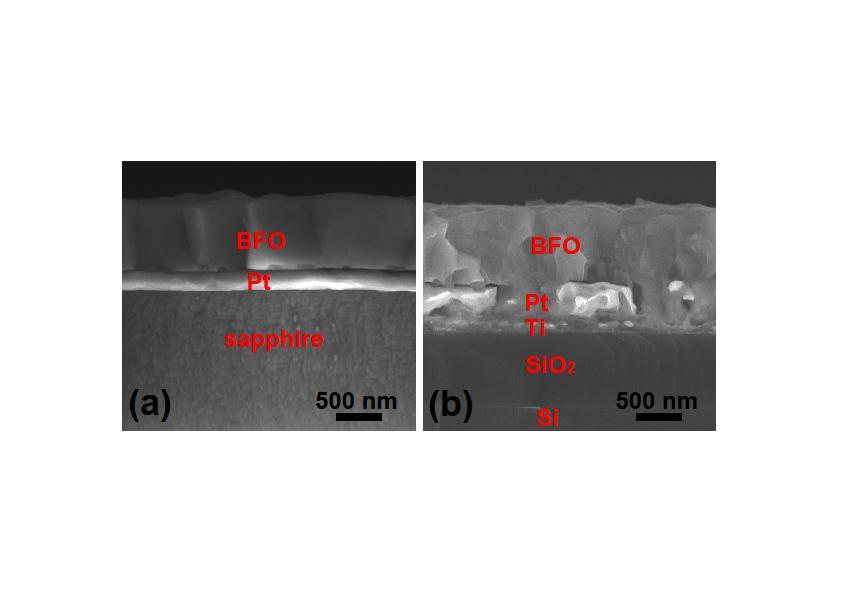
3 Scanning Electron Microscope (SEM) was used to examine the microstructure of the BFO on different substrates. For electric measurements, Au top electrodes with an area of 0.1 mm 2 were sputtered using a metal shadow mask. The current-voltage (I-V) curves were recorded with a Keithley 2400 source meter. 3. RESULTS AND DISCUSSIONS The surface morphology images measured by AFM on the samples after heating the substrate and with and without depositing the BFO thin film are shown in Fig. 1. The BFO thin film on Pt/sapphire exhibits an average grain size of ~120 nm [Fig. 1(a)], which is much smaller than that on Pt/Ti/SiO 2 /Si [Fig. 1(c)]. Moreover, the BFO surface roughness is only 1 nm on Pt/sapphire, while it is increased to 12.2 nm by using Pt/Ti/SiO 2 /Si substrates. The apparent change of the BFO topography is due to the distinct bottom electrode surface after the thin film growth at high temperature. As shown in Fig. 1(b) and (d), the surface roughness of the Pt bottom electrode amounts to 1.4 nm and 10.4 nm on sapphire and Ti/SiO 2 /Si, respectively. The morphology of the Pt surface significantly influences the electrical properties of the BFO thin films, which will be discussed later. The SEM cross section images are shown in Fig. 2. As expected for the same PLD growth conditions, the BFO thin films have a similar thickness of ~500 nm on both substrates. A sharp interface between the film and the Pt bottom electrode can be observed on sapphire substrates. However, the interface is rather rough for BFO on Pt/Ti/SiO 2 /Si substrate, which is likely due to the interdiffusion caused by the high growth temperature. High quality interfaces on Pt/sapphire substrates have also been reported in chemical solution prepared BFO thin films. 8 It is noticed that the columnar grains extend from the bottom electrode throughout the whole thin film on 3
4 Pt/sapphire [Fig. 2(a)], however, the film on Pt/Ti/SiO 2 /Si consists of multi-layer grains [Fig. 2(b)]. I-V curves of the BFO thin films on Pt/sapphire and Pt/Ti/SiO 2 /Si are shown in Fig. 3(a). Although the BFO growth conditions and the evaporation of the top contact are the same, significant differences can be observed in the I-V curves. First of all, the thin film on Pt/sapphire shows a symmetric I-V curve, while that on Pt/Ti/SiO 2 /Si has a rectifying I-V characteristic. Moreover, the leakage current of the former one is much lower in positive bias range. In the negative bias, the leakage currents of the BFO films on different substrates are comparable. Finally and also most interesting, only the thin film on Pt/Ti/SiO 2 /Si shows a hysteresis behavior, indicating that it is resistively switchable. The positive bias sets the film to LRS, and the negative bias resets it back to HRS. To understand the difference of the I-V characteristics, it is necessary to investigate the conduction mechanisms of those thin films. As shown in Fig. 3(b), linear fittings are obtained for the film on Pt/sapphire substrates in both voltage polarities in a log(j) ~ E 0.5 scale. Note that only one branch is fitted for each voltage polarity, since there is no hysteresis. However, for the film on Pt/Ti/SiO 2 /Si substrate, linear fitting is only possible in negative bias range [Fig. 3(b)]. By using the Schottky emission equation: * J A T 2 b exp ( kt q kt qe ) 4 K 0 (1) optical dielectric constants (K) are calculated to be 5.91 (positive bias) and 6.39 (negative bias) for the film on Pt/sapphire, and 6.85 (negative bias) on Pt/Ti/SiO 2 /Si. These values are in good agreement with the previous report that K is 6.25 for BFO thin films, 9 indicating that the Schottky emission is the dominant conduction mechanism in these voltage ranges for different samples. 4
5 Therefore, the symmetric I-V curve of the thin film on Pt/sapphire substrate is likely due to the formation of Schottky contacts at both interfaces, 10 while the rectifying behavior of the thin film on Pt/Ti/SiO2/Si is because of the asymmetric contact barriers at the two interfaces. Note that the comparable leakage current in the negative bias range for the thin films on different substrates is likely due to the same conduction mechanism when the interface between BFO thin film and top contact is involved, i.e. the Schottky junction at the top interface shows a very similar conduction behavior. However, an obvious hysteresis behavior is observed in the positive bias range of the thin film on Pt/Ti/SiO 2 /Si substrate [Fig. 3(a)]. In contrast to the Schottky emission in the negative bias range [Fig. 3(b)], two different types of conduction mechanisms dominate the upper (LRS) and lower (HRS) I-V branches, respectively. The lower branch, i.e. the HRS, can be well fitted using the Poole-Frenkel model, which deduces an optical dielectric constant (K) of 5.02 [Fig. 3(c)]. Since PF conduction is bulk-limited, the contact resistance of the bottom interface is much smaller than the bulk thin film, and the bottom contact behaves like an Ohmic contact, which results from the rough bottom Pt surface [Fig. 1(d)] and the interdiffusion at the BFO/Pt interface [Fig. 2(b)] Note that although the top interface is a Schottky contact, it is not possible to obtain a reasonable fitting by using the forward Schottky emission model. Therefore, the resistance of the top interface is also negligible as compared to the bulk thin film when it is forward biased. However, when the voltage is large enough, the fitting deviates from the PF model, and tunneling starts to appear as indicated by the negative slope of the linear fitting in a log(j/e 2 ) ~ 1/E scale [Fig. 3(d)]. Furthermore, the upper branch (LRS) is also dominated by tunneling as revealed by the fitting [Fig. 3(d)]. This suggests that when the thin film is set to LRS, the bulk resistance of the thin film is 5
6 significantly decreased, and the interface resistance (tunneling effect) becomes dominant. Because the bottom interface is Ohmic contact, tunneling takes place at the top interface, revealing that the depletion region at the Au/BFO interface is considerably narrowed. Note that the small hysteresis in the negative bias range is likely due to the thin depletion thickness induced by the positive bias, the deviation of the fitting in Fig. 3(b) can be attributed to the presence of tunneling through the depletion layer. By further increasing the negative bias, the depletion region is extended, which eliminates the tunneling, and only Schottky emission dominates. As discussed above, the resistive switching of the thin film on Pt/Ti/SiO 2 /Si substrate is due to the nonvolatile modification of the depletion thickness at the top interface (Au/BFO) together with the resistance change of the bulk thin film. However, the physical origin of this nonvolatile effect needs to be clarified. Ion migration model has been proposed in a wide range of resistive switching behaviors in various materials. However, when taking into account the polarities for the two resistance states, the ion migration model is not applicable. The most movable ions in BFO thin films are oxygen vacancies (OVs), which are donors since they provide electrons. 11 If a positive bias is applied on the top Au electrode, the OVs are pushed away from the Au/BFO interface since they are positively charged. That should raise the barrier height, because the concentration of donors is decreased at the interface. Thus the positive bias sets the structure to HRS if the ion migration model dominates, which is just the opposite of our observation as shown in Fig. 3(a). By comparing the I-V characteristics of those thin films on different substrates, the nonvolatile resistive switching is likely due to a pure electronic effect, i. e. the electron trapping effect. No resistive switching has been observed in the thin film on Pt/sapphire substrate, because the two Schottky interfaces block the electron injection in both voltage polarities. And only the 6
7 thin film on Pt/Ti/SiO 2 /Si shows an obvious resistive switching in the positive bias range, due to the large amount of injected electrons through the Ohmic BFO/Pt contact. 4. CONCLUSIONS In summary, BiFeO 3 thin films have been deposited on Pt/sapphire and Pt/Ti/SiO 2 /Si substrates, respectively. The Schottky contacts of the thin film on Pt/sapphire dominate the transport and help to suppress the leakage current in both voltage polarities, and the I-V curve shows no hysteresis due to the reversely biased Schottky contact. However, the thin film on Pt/Ti/SiO 2 /Si shows a diode behavior and is resistively switchable, which results from the asymmetric contact geometry at the two interfaces. By comparing the electric properties of the thin films on different substrates, the mechanism of the observed resistive switching is clarified to be due to an electron trapping effect. ACKNOWLEDGMENTS Y. S. would like to thank the China Scholarship Council (grant number: ). S. Z. acknowledges the funding by the Helmholtz-Gemeinschaft Deutscher Forschungszentren (HGF-VH-NG-713). D. B. and H. S. thank the financial support from the Bundesministerium für Bildung und Forschung (BMBF grant number: 13N10144). REFERENCES [1] D. S. Jeong, H. Schroeder, U. Breuer, and R. Waser, J. Appl. Phys. 104, (2008). [2] D. Ielmini, F Nardi, and C. Cagli, Nanotechnology 22, (2011). [3] X. Cao, X. Li, X. Gao, X. Liu, C. Yang, R. Yang, and P. Jin, J. Phys. D: Appl. Phys. 44, 7
8 (2011). [4] A. Sawa, T. Fujii, M. Kawasaki, and Y. Tokura, Appl. Phys. Lett. 85, 4073 (2004). [5] R. Muenstermann, T. Menke, R. Dittmann, S. Mi, C.-L. Jia, D. Park, and J. Mayer, J. Appl. Phys. 108, (2010). [6] Y. Shuai, S. Zhou, D. Bürger, M. Helm, and H. Schmidt, J. Appl. Phys. 109, (2011). [7] Y. Shuai, S. Zhou, C. Wu, W. Zhang, D. Bürger, S. Slesazeck, T. Mikolajick, M. Helm, and H. Schmidt, Appl. Phys. Express. 4, (2011). [8] S. K. Singh, H. Ishiwara, and K. Maruyama, J. Appl. Phys. 100, (2006). [9] S. Iakovlev, C.-H. Solterbeck, M. Kuhnke, and M. Es-Souni, J. Appl. Phys. 97, (2005). [10] Y. Shuai, S. Zhou, S. Streit, H. Reuther, D. Bürger, S. Slesazeck, T. Mikolajick, M. Helm, and H. Schmidt, Appl. Phys. Lett. 98, (2011). [11] C.-H. Yang, J. Seidel, S. Y. Kim, P. B. Rossen, P. Yu, M. Gajek, Y. H. Chu, L. W. Martin, M. B. Holcomb, Q. He, P. Maksymovych, N. Balke, S. V. Kalinin, A. P. Baddorf, S. R. Basu, M. L. Scullin, and R. Ramesh, Nat. Mater. 8, 485 (2009). 8
9 Figure captions: Fig. 1. AFM surface images of the heated Pt/sapphire and Pt/Ti/SiO 2 /Si substrates with (a,c) and without (b,d) BFO thin film growth. Fig. 2. SEM cross section images of the BFO thin films on Pt/sapphire (a), and on Pt/Ti/SiO 2 /Si (b). Fig. 3. (a) I-V curves of the BFO thin films on Pt/sapphire and on Pt/Ti/SiO2/Si substrates, respectively. (b) Log J ~ E 0.5 scale representing Schottky emission. (c) Log (J/E) ~ E 0.5 scale representing Poole-Frankel conduction. (d) Log (J/E 2 ) ~ 1/E scale representing tunneling. 9

10 Figures Fig. 1 Fig. 2 10
11 Fig. 3 11
Supplementary Information. implantation of bottom electrodes
 Supplementary Information Engineering interface-type resistive switching in BiFeO3 thin film switches by Ti implantation of bottom electrodes Tiangui You, 1,2 Xin Ou, 1,* Gang Niu, 3 Florian Bärwolf, 3
Supporting Information
 Supporting Information Inverse I-V injection characteristics of ZnO nanoparticle based diodes Paul Mundt 1,2, Stefan Vogel 3, Klaus Bonrad 2,4, Heinz von Seggern 1 * Technische Universität Darmstadt 1
CHAPTER 9 CURRENT VOLTAGE CHARACTERISTICS
 CHAPTER 9 CURRENT VOLTAGE CHARACTERISTICS 9.1 INTRODUCTION The phthalocyanines are a class of organic materials which are generally thermally stable and may be deposited as thin films by vacuum evaporation
Supplementary Information
 Supplementary Information For Nearly Lattice Matched All Wurtzite CdSe/ZnTe Type II Core-Shell Nanowires with Epitaxial Interfaces for Photovoltaics Kai Wang, Satish C. Rai,Jason Marmon, Jiajun Chen, Kun
Supporting Information. Vertical Graphene-Base Hot-Electron Transistor
 Supporting Information Vertical Graphene-Base Hot-Electron Transistor Caifu Zeng, Emil B. Song, Minsheng Wang, Sejoon Lee, Carlos M. Torres Jr., Jianshi Tang, Bruce H. Weiller, and Kang L. Wang Department
A scanning tunneling microscopy based potentiometry technique and its application to the local sensing of the spin Hall effect
 A scanning tunneling microscopy based potentiometry technique and its application to the local sensing of the spin Hall effect Ting Xie 1, a), Michael Dreyer 2, David Bowen 3, Dan Hinkel 3, R. E. Butera
SUPPLEMENTARY INFORMATION
 Room-temperature continuous-wave electrically injected InGaN-based laser directly grown on Si Authors: Yi Sun 1,2, Kun Zhou 1, Qian Sun 1 *, Jianping Liu 1, Meixin Feng 1, Zengcheng Li 1, Yu Zhou 1, Liqun
Design, Fabrication and Characterization of Very Small Aperture Lasers
 372 Progress In Electromagnetics Research Symposium 2005, Hangzhou, China, August 22-26 Design, Fabrication and Characterization of Very Small Aperture Lasers Jiying Xu, Jia Wang, and Qian Tian Tsinghua
HfO 2 Based Resistive Switching Non-Volatile Memory (RRAM) and Its Potential for Embedded Applications
 and Its Potential for Embedded Applications") 2012 International Conference on Solid-State and Integrated Circuit (ICSIC 2012) IPCSIT vol. 32 (2012) (2012) IACSIT Press, Singapore HfO 2 Based Resistive Switching Non-Volatile Memory (RRAM) and Its
2012 International Conference on Solid-State and Integrated Circuit (ICSIC 2012) IPCSIT vol. 32 (2012) (2012) IACSIT Press, Singapore HfO 2 Based Resistive Switching Non-Volatile Memory (RRAM) and Its
Conductance switching in Ag 2 S devices fabricated by sulphurization
 3 Conductance switching in Ag S devices fabricated by sulphurization The electrical characterization and switching properties of the α-ag S thin films fabricated by sulfurization are presented in this
Resistive Switching Mechanisms on TaO x and SrRuO 3 Thin Film Surfaces Probed by Scanning Tunneling Microscopy
 Resistive Switching Mechanisms on TaO x and SrRuO 3 Thin Film Surfaces Probed by Scanning Tunneling Microscopy Marco Moors, 1# Kiran Kumar Adepalli, 2,3# Qiyang Lu, 3 Anja Wedig, 1 Christoph Bäumer, 1
Supplementary Figure 1 High-resolution transmission electron micrograph of the
 Supplementary Figure 1 High-resolution transmission electron micrograph of the LAO/STO structure. LAO/STO interface indicated by the dotted line was atomically sharp and dislocation-free. Supplementary
JOURNAL OF APPLIED PHYSICS 99,
 JOURNAL OF APPLIED PHYSICS 99, 014501 2006 Demonstration and analysis of reduced reverse-bias leakage current via design of nitride semiconductor heterostructures grown by molecular-beam epitaxy H. Zhang
Supplementary Figure 1 Schematic illustration of fabrication procedure of MoS2/h- BN/graphene heterostructures. a, c d Supplementary Figure 2
 Supplementary Figure 1 Schematic illustration of fabrication procedure of MoS 2 /hon a 300- BN/graphene heterostructures. a, CVD-grown b, Graphene was patterned into graphene strips by oxygen monolayer
Supporting Information
 Supporting Information Resistive Switching Memory Effects of NiO Nanowire/Metal Junctions Keisuke Oka 1, Takeshi Yanagida 1,2 *, Kazuki Nagashima 1, Tomoji Kawai 1,3 *, Jin-Soo Kim 3 and Bae Ho Park 3
Analog Synaptic Behavior of a Silicon Nitride Memristor
 Supporting Information Analog Synaptic Behavior of a Silicon Nitride Memristor Sungjun Kim, *, Hyungjin Kim, Sungmin Hwang, Min-Hwi Kim, Yao-Feng Chang,, and Byung-Gook Park *, Inter-university Semiconductor
Resistive switching in perovskite-oxide capacitor-type devices. IEEE Transactions on Magnetics, 2014, v. 50 n. 7, article no.
 Title Resistive switching in perovskite-oxide capacitor-type devices Author(s) Luo, Z; Lau, HK; Chan, PKL; Leung, CW Citation IEEE Transactions on Magnetics, 2014, v. 50 n. 7, article no. 3000904 Issued
Three Terminal Devices
 Three Terminal Devices - field effect transistor (FET) - bipolar junction transistor (BJT) - foundation on which modern electronics is built - active devices - devices described completely by considering
E LECTROOPTICAL(EO)modulatorsarekeydevicesinoptical
modulatorsarekeydevicesinoptical") 286 JOURNAL OF LIGHTWAVE TECHNOLOGY, VOL. 26, NO. 2, JANUARY 15, 2008 Design and Fabrication of Sidewalls-Extended Electrode Configuration for Ridged Lithium Niobate Electrooptical Modulator Yi-Kuei Wu,
286 JOURNAL OF LIGHTWAVE TECHNOLOGY, VOL. 26, NO. 2, JANUARY 15, 2008 Design and Fabrication of Sidewalls-Extended Electrode Configuration for Ridged Lithium Niobate Electrooptical Modulator Yi-Kuei Wu,
Supplementary Materials for
 www.sciencemag.org/cgi/content/full/science.1234855/dc1 Supplementary Materials for Taxel-Addressable Matrix of Vertical-Nanowire Piezotronic Transistors for Active/Adaptive Tactile Imaging Wenzhuo Wu,
Electrical transport properties in self-assembled erbium. disilicide nanowires
 Solid State Phenomena Online: 2007-03-15 ISSN: 1662-9779, Vols. 121-123, pp 413-416 doi:10.4028/www.scientific.net/ssp.121-123.413 2007 Trans Tech Publications, Switzerland Electrical transport properties
photolithographic techniques (1). Molybdenum electrodes (50 nm thick) are deposited by
. Molybdenum electrodes (50 nm thick) are deposited by") Supporting online material Materials and Methods Single-walled carbon nanotube (SWNT) devices are fabricated using standard photolithographic techniques (1). Molybdenum electrodes (50 nm thick) are deposited
Supporting online material Materials and Methods Single-walled carbon nanotube (SWNT) devices are fabricated using standard photolithographic techniques (1). Molybdenum electrodes (50 nm thick) are deposited
Supporting Information
 Supporting Information Fabrication of High-Performance Ultrathin In 2 O 3 Film Field-Effect Transistors and Biosensors Using Chemical Lift-Off Lithography Jaemyung Kim,,,# You Seung Rim,,,# Huajun Chen,,
Depletion width measurement in an organic Schottky contact using a Metal-
 Depletion width measurement in an organic Schottky contact using a Metal- Semiconductor Field-Effect Transistor Arash Takshi, Alexandros Dimopoulos and John D. Madden Department of Electrical and Computer
Integrated diodes. The forward voltage drop only slightly depends on the forward current. ELEKTRONIKOS ĮTAISAI
 1 Integrated diodes pn junctions of transistor structures can be used as integrated diodes. The choice of the junction is limited by the considerations of switching speed and breakdown voltage. The forward
Fabrication of a submicron patterned using an electrospun single fiber as mask. Author(s)Ishii, Yuya; Sakai, Heisuke; Murata,
Ishii, Yuya; Sakai, Heisuke; Murata,") JAIST Reposi https://dspace.j Title Fabrication of a submicron patterned using an electrospun single fiber as mask Author(s)Ishii, Yuya; Sakai, Heisuke; Murata, Citation Thin Solid Films, 518(2): 647-650
JAIST Reposi https://dspace.j Title Fabrication of a submicron patterned using an electrospun single fiber as mask Author(s)Ishii, Yuya; Sakai, Heisuke; Murata, Citation Thin Solid Films, 518(2): 647-650
Gallium nitride (GaN)
") 80 Technology focus: GaN power electronics Vertical, CMOS and dual-gate approaches to gallium nitride power electronics US research company HRL Laboratories has published a number of papers concerning
80 Technology focus: GaN power electronics Vertical, CMOS and dual-gate approaches to gallium nitride power electronics US research company HRL Laboratories has published a number of papers concerning
Supporting Information. Air-stable surface charge transfer doping of MoS 2 by benzyl viologen
 Supporting Information Air-stable surface charge transfer doping of MoS 2 by benzyl viologen Daisuke Kiriya,,ǁ, Mahmut Tosun,,ǁ, Peida Zhao,,ǁ, Jeong Seuk Kang, and Ali Javey,,ǁ,* Electrical Engineering
Sub-Threshold Region Behavior of Long Channel MOSFET
 Sub-threshold Region - So far, we have discussed the MOSFET behavior in linear region and saturation region - Sub-threshold region is refer to region where Vt is less than Vt - Sub-threshold region reflects
Transparent p-type SnO Nanowires with Unprecedented Hole Mobility among Oxide Semiconductors
 Supplementary Information Transparent p-type SnO Nanowires with Unprecedented Hole Mobility among Oxide Semiconductors J. A. Caraveo-Frescas and H. N. Alshareef* Materials Science and Engineering, King
3D Vertical Dual-Layer Oxide Memristive Devices for Neuromorphic Computing
 3D Vertical Dual-Layer Oxide Memristive Devices for Neuromorphic Computing Siddharth Gaba, Patrick Sheridan, Chao Du, and Wei Lu* Electrical Engineering and Computer Science, University of Michigan, Ann
EXPERIMENT 10: SCHOTTKY DIODE CHARACTERISTICS
 EXPERIMENT 10: SCHOTTKY DIODE CHARACTERISTICS AIM: To plot forward and reverse characteristics of Schottky diode (Metal Semiconductor junction) APPARATUS: D.C. Supply (0 15 V), current limiting resistor
Semiconductor Devices Lecture 5, pn-junction Diode
 Semiconductor Devices Lecture 5, pn-junction Diode Content Contact potential Space charge region, Electric Field, depletion depth Current-Voltage characteristic Depletion layer capacitance Diffusion capacitance
Solid State Devices- Part- II. Module- IV
 Solid State Devices- Part- II Module- IV MOS Capacitor Two terminal MOS device MOS = Metal- Oxide- Semiconductor MOS capacitor - the heart of the MOSFET The MOS capacitor is used to induce charge at the
High Performance Visible-Blind Ultraviolet Photodetector Based on
 Supplementary Information High Performance Visible-Blind Ultraviolet Photodetector Based on IGZO TFT Coupled with p-n Heterojunction Jingjing Yu a,b, Kashif Javaid b,c, Lingyan Liang b,*, Weihua Wu a,b,
ELECTRICAL PROPERTIES OF POROUS SILICON PREPARED BY PHOTOCHEMICAL ETCHING ABSTRACT
 ELECTRICAL PROPERTIES OF POROUS SILICON PREPARED BY PHOTOCHEMICAL ETCHING A. M. Ahmmed 1, A. M. Alwan 1, N. M. Ahmed 2 1 School of Applied Science/ University of Technology, Baghdad-IRAQ 2 School of physics/
SUPPLEMENTARY INFORMATION
 SUPPLEMENTARY INFORMATION Dopant profiling and surface analysis of silicon nanowires using capacitance-voltage measurements Erik C. Garnett 1, Yu-Chih Tseng 4, Devesh Khanal 2,3, Junqiao Wu 2,3, Jeffrey
Study of shear force as a distance regulation mechanism for scanning near-field optical microscopy
 Study of shear force as a distance regulation mechanism for scanning near-field optical microscopy C. Durkan a) and I. V. Shvets Department of Physics, Trinity College Dublin, Ireland Received 31 May 1995;
Wu Lu Department of Electrical and Computer Engineering and Microelectronics Laboratory, University of Illinois, Urbana, Illinois 61801
 Comparative study of self-aligned and nonself-aligned SiGe p-metal oxide semiconductor modulation-doped field effect transistors with nanometer gate lengths Wu Lu Department of Electrical and Computer
Logic circuits based on carbon nanotubes
 Available online at www.sciencedirect.com Physica E 16 (23) 42 46 www.elsevier.com/locate/physe Logic circuits based on carbon nanotubes A. Bachtold a;b;, P. Hadley a, T. Nakanishi a, C. Dekker a a Department
Machine-Aligned Fabrication of Submicron SIS Tunnel Junctions Using a Focused Ion Beam
 Machine-Aligned Fabrication of Submicron SIS Tunnel Junctions Using a Focused Ion Beam Robert. B. Bass, Jian. Z. Zhang and Aurthur. W. Lichtenberger Department of Electrical Engineering, University of
High-Speed Scalable Silicon-MoS 2 P-N Heterojunction Photodetectors
 High-Speed Scalable Silicon-MoS 2 P-N Heterojunction Photodetectors Veerendra Dhyani 1, and Samaresh Das 1* 1 Centre for Applied Research in Electronics, Indian Institute of Technology Delhi, New Delhi-110016,
High-Ohmic Resistors using Nanometer-Thin Pure-Boron Chemical-Vapour-Deposited Layers
 High-Ohmic Resistors using Nanometer-Thin Pure-Boron Chemical-Vapour-Deposited Layers Negin Golshani, Vahid Mohammadi, Siva Ramesh, Lis K. Nanver Delft University of Technology The Netherlands ESSDERC
Supporting Information. Epitaxially Aligned Cuprous Oxide Nanowires for All-Oxide, Single-Wire Solar Cells
 Supporting Information Epitaxially Aligned Cuprous Oxide Nanowires for All-Oxide, Single-Wire Solar Cells Sarah Brittman, 1,2 Youngdong Yoo, 1 Neil P. Dasgupta, 1,3 Si-in Kim, 4 Bongsoo Kim, 4 and Peidong
Esaki diodes in van der Waals heterojunctions with broken-gap energy band alignment
 Supplementary information for Esaki diodes in van der Waals heterojunctions with broken-gap energy band alignment Rusen Yan 1,2*, Sara Fathipour 2, Yimo Han 4, Bo Song 1,2, Shudong Xiao 1, Mingda Li 1,
Lecture 18: Photodetectors
 Lecture 18: Photodetectors Contents 1 Introduction 1 2 Photodetector principle 2 3 Photoconductor 4 4 Photodiodes 6 4.1 Heterojunction photodiode.................... 8 4.2 Metal-semiconductor photodiode................
Experiment 3 - IC Resistors
 Experiment 3 - IC Resistors.T. Yeung, Y. Shin,.Y. Leung and R.T. Howe UC Berkeley EE 105 1.0 Objective This lab introduces the Micro Linear Lab Chips, with measurements of IC resistors and a distributed
2 EXPERIMENTAL PROCEDURE Multilayer OLEDs manufactured by the Eastman-Kodak Company are used in the development of the models presented in this paper.
 OLED MODELING VIA SPICE J. P. Bender, B. J. Norris, and J. F. Wager Department of Electrical and Computer Engineering Center for Advanced Materials Research Oregon State University Corvallis, OR 97331-3211
Fabrication of High-Speed Resonant Cavity Enhanced Schottky Photodiodes
 Fabrication of High-Speed Resonant Cavity Enhanced Schottky Photodiodes Abstract We report the fabrication and testing of a GaAs-based high-speed resonant cavity enhanced (RCE) Schottky photodiode. The
Supporting Information
 Electronic Supplementary Material (ESI) for Materials Horizons. This journal is The Royal Society of Chemistry 2017 Supporting Information Nanofocusing of circularly polarized Bessel-type plasmon polaritons
Fabrication and electrical characterization of MONOS memory with novel high-κ gate stack
 Title Fabrication and electrical characterization of MONOS memory with novel high-κ gate stack Author(s) Liu, L; Xu, JP; Chan, CL; Lai, PT Citation The IEEE International Conference on Electron Devices
Zinc Oxide Nanowires Impregnated with Platinum and Gold Nanoparticle for Ethanol Sensor
 CMU. J.Nat.Sci. Special Issue on Nanotechnology (2008) Vol. 7(1) 185 Zinc Oxide Nanowires Impregnated with Platinum and Gold Nanoparticle for Ethanol Sensor Weerayut Wongka, Sasitorn Yata, Atcharawan Gardchareon,
Power MOSFET Zheng Yang (ERF 3017,
 ECE442 Power Semiconductor Devices and Integrated Circuits Power MOSFET Zheng Yang (ERF 3017, email: yangzhen@uic.edu) Evolution of low-voltage (
Nano-structured superconducting single-photon detector
 Nano-structured superconducting single-photon detector G. Gol'tsman *a, A. Korneev a,v. Izbenko a, K. Smirnov a, P. Kouminov a, B. Voronov a, A. Verevkin b, J. Zhang b, A. Pearlman b, W. Slysz b, and R.
Spectrally Selective Photocapacitance Modulation in Plasmonic Nanochannels for Infrared Imaging
 Supporting Information Spectrally Selective Photocapacitance Modulation in Plasmonic Nanochannels for Infrared Imaging Ya-Lun Ho, Li-Chung Huang, and Jean-Jacques Delaunay* Department of Mechanical Engineering,
Bistability in Bipolar Cascade VCSELs
 Bistability in Bipolar Cascade VCSELs Thomas Knödl Measurement results on the formation of bistability loops in the light versus current and current versus voltage characteristics of two-stage bipolar
A Broadband High-Efficiency Rectifier Based on Two-Level Impedance Match Network
 Progress In Electromagnetics Research Letters, Vol. 72, 91 97, 2018 A Broadband High-Efficiency Rectifier Based on Two-Level Impedance Match Network Ling-Feng Li 1, Xue-Xia Yang 1, 2, *,ander-jialiu 1
SQUID Test Structures Presented by Makoto Ishikawa
 SQUID Test Structures Presented by Makoto Ishikawa We need to optimize the microfabrication process for making an SIS tunnel junction because it is such an important structure in a SQUID. Figure 1 is a
NAME: Last First Signature
 UNIVERSITY OF CALIFORNIA, BERKELEY College of Engineering Department of Electrical Engineering and Computer Sciences EE 130: IC Devices Spring 2003 FINAL EXAMINATION NAME: Last First Signature STUDENT
Influence of dielectric substrate on the responsivity of microstrip dipole-antenna-coupled infrared microbolometers
 Influence of dielectric substrate on the responsivity of microstrip dipole-antenna-coupled infrared microbolometers Iulian Codreanu and Glenn D. Boreman We report on the influence of the dielectric substrate
Atomic-layer deposition of ultrathin gate dielectrics and Si new functional devices
 Atomic-layer deposition of ultrathin gate dielectrics and Si new functional devices Anri Nakajima Research Center for Nanodevices and Systems, Hiroshima University 1-4-2 Kagamiyama, Higashi-Hiroshima,
FIG. 1: (a) Schematic of the device showing the material stack and relative thickness of each layer. (b) I-V switching characteristics of the device.
 Schematic of the device showing the material stack and relative thickness of each layer. (b) I-V switching characteristics of the device.") Pulse Width and Height Modulation for Multi-level Resistance in bi-layer TaO x based RRAM Zahiruddin Alamgir, 1 Karsten Beckmann, 1 Joshua Holt, 1 and Nathaniel C. Cady 1 Colleges of Nanoscale Science
Pulse Width and Height Modulation for Multi-level Resistance in bi-layer TaO x based RRAM Zahiruddin Alamgir, 1 Karsten Beckmann, 1 Joshua Holt, 1 and Nathaniel C. Cady 1 Colleges of Nanoscale Science
Semiconductor Physics and Devices
 Metal-Semiconductor and Semiconductor Heterojunctions The Metal-Oxide-Semiconductor Field-Effect Transistor (MOSFET) is one of two major types of transistors. The MOSFET is used in digital circuit, because
2014, IJARCSSE All Rights Reserved Page 1352
 Volume 4, Issue 3, March 2014 ISSN: 2277 128X International Journal of Advanced Research in Computer Science and Software Engineering Research Paper Available online at: www.ijarcsse.com Double Gate N-MOSFET
Proposal of Novel Collector Structure for Thin-wafer IGBTs
 12 Special Issue Recent R&D Activities of Power Devices for Hybrid ElectricVehicles Research Report Proposal of Novel Collector Structure for Thin-wafer IGBTs Takahide Sugiyama, Hiroyuki Ueda, Masayasu
Key Questions. ECE 340 Lecture 39 : Introduction to the BJT-II 4/28/14. Class Outline: Fabrication of BJTs BJT Operation
 Things you should know when you leave ECE 340 Lecture 39 : Introduction to the BJT-II Fabrication of BJTs Class Outline: Key Questions What elements make up the base current? What do the carrier distributions
Reconfigurable Si-Nanowire Devices
 Reconfigurable Si-Nanowire Devices André Heinzig, Walter M. Weber, Dominik Martin, Jens Trommer, Markus König and Thomas Mikolajick andre.heinzig@namlab.com log I d Present CMOS technology ~ 88 % of IC
THERMIONIC AND GASEOUS STATE DIODES
 THERMIONIC AND GASEOUS STATE DIODES Thermionic and gaseous state (vacuum tube) diodes Thermionic diodes are thermionic-valve devices (also known as vacuum tubes, tubes, or valves), which are arrangements
Power generation with laterally-packaged piezoelectric fine wires
 Supplementary materials Power generation with laterally-packaged piezoelectric fine wires Rusen Yang 1, Yong Qin 1, Liming Dai 2 and Zhong Lin Wang 1, * 1 School of Materials Science and Engineering, Georgia
Gigahertz Ambipolar Frequency Multiplier Based on Cvd Graphene
 Gigahertz Ambipolar Frequency Multiplier Based on Cvd Graphene The MIT Faculty has made this article openly available. Please share how this access benefits you. Your story matters. Citation As Published
Design and Analysis of Double Gate MOSFET Devices using High-k Dielectric
 International Journal of Electrical Engineering. ISSN 0974-2158 Volume 7, Number 1 (2014), pp. 53-60 International Research Publication House http://www.irphouse.com Design and Analysis of Double Gate
Author(s) Osamu; Nakamura, Tatsuya; Katagiri,
 Osamu; Nakamura, Tatsuya; Katagiri,") TitleCryogenic InSb detector for radiati Author(s) Kanno, Ikuo; Yoshihara, Fumiki; Nou Osamu; Nakamura, Tatsuya; Katagiri, Citation REVIEW OF SCIENTIFIC INSTRUMENTS (2 2533-2536 Issue Date 2002-07 URL
TitleCryogenic InSb detector for radiati Author(s) Kanno, Ikuo; Yoshihara, Fumiki; Nou Osamu; Nakamura, Tatsuya; Katagiri, Citation REVIEW OF SCIENTIFIC INSTRUMENTS (2 2533-2536 Issue Date 2002-07 URL
Nanofluidic Diodes based on Nanotube Heterojunctions
 Supporting Information Nanofluidic Diodes based on Nanotube Heterojunctions Ruoxue Yan, Wenjie Liang, Rong Fan, Peidong Yang 1 Department of Chemistry, University of California, Berkeley, CA 94720, USA
SUPPLEMENTARY INFORMATION
 SUPPLEMENTARY INFORMATION doi: 10.1038/nmat797 Spin injection/detection via an organic-based magnetic semiconductor Jung-Woo Yoo 1,, Chia-Yi Chen 3, H. W. Jang 4, C. W. Bark 4, V. N. Prigodin 1, C. B.
SUPPLEMENTARY INFORMATION
 In the format provided by the authors and unedited. Photon-triggered nanowire transistors Jungkil Kim, Hoo-Cheol Lee, Kyoung-Ho Kim, Min-Soo Hwang, Jin-Sung Park, Jung Min Lee, Jae-Pil So, Jae-Hyuck Choi,
Supplementary Information: Nanoscale. Structure, Dynamics, and Aging Behavior of. Metallic Glass Thin Films
 Supplementary Information: Nanoscale Structure, Dynamics, and Aging Behavior of Metallic Glass Thin Films J.A.J. Burgess,,, C.M.B. Holt,, E.J. Luber,, D.C. Fortin, G. Popowich, B. Zahiri,, P. Concepcion,
IMAGING P-N JUNCTIONS BY SCANNING NEAR-FIELD OPTICAL, ATOMIC FORCE AND ELECTRICAL CONTRAST MICROSCOPY. G. Tallarida Laboratorio MDM-INFM
 Laboratorio MDM - INFM Via C.Olivetti 2, I-20041 Agrate Brianza (MI) M D M Materiali e Dispositivi per la Microelettronica IMAGING P-N JUNCTIONS BY SCANNING NEAR-FIELD OPTICAL, ATOMIC FORCE AND ELECTRICAL
Vertical Nanowall Array Covered Silicon Solar Cells
 International Conference on Solid-State and Integrated Circuit (ICSIC ) IPCSIT vol. () () IACSIT Press, Singapore Vertical Nanowall Array Covered Silicon Solar Cells J. Wang, N. Singh, G. Q. Lo, and D.
Single Nanoparticle Plasmonic Electro-Optic Modulator Based on MoS 2 Monolayers
 Single Nanoparticle Plasmonic Electro-Optic Modulator Based on MoS 2 Monolayers Bowen Li,, Shuai Zu,, Jiadong Zhou, Qiao Jiang, Bowen Du, Hangyong Shan, Yang Luo, Zheng Liu, Xing Zhu, and Zheyu Fang,*
Body-Biased Complementary Logic Implemented Using AlN Piezoelectric MEMS Switches
 University of Pennsylvania From the SelectedWorks of Nipun Sinha 29 Body-Biased Complementary Logic Implemented Using AlN Piezoelectric MEMS Switches Nipun Sinha, University of Pennsylvania Timothy S.
Investigation of the Near-field Distribution at Novel Nanometric Aperture Laser
 Investigation of the Near-field Distribution at Novel Nanometric Aperture Laser Tiejun Xu, Jia Wang, Liqun Sun, Jiying Xu, Qian Tian Presented at the th International Conference on Electronic Materials
arxiv: v1 [cond-mat.mtrl-sci] 22 Feb 2011
![arxiv: v1 [cond-mat.mtrl-sci] 22 Feb 2011](/thumbs/73/69071165.jpg "arxiv: v1 [cond-mat.mtrl-sci] 22 Feb 2011") Asymmetric pulsing for reliable operation of titanium/manganite memristors F. Gomez-Marlasca 1, N. Ghenzi 1, P. Stoliar 1,2,, M. arxiv:1102.4554v1 [cond-mat.mtrl-sci] 22 Feb 2011 J. Sánchez 3, M. J. Rozenberg
Asymmetric pulsing for reliable operation of titanium/manganite memristors F. Gomez-Marlasca 1, N. Ghenzi 1, P. Stoliar 1,2,, M. arxiv:1102.4554v1 [cond-mat.mtrl-sci] 22 Feb 2011 J. Sánchez 3, M. J. Rozenberg
Robert G. Hunsperger. Integrated Optics. Theory and Technology. Sixth Edition. 4ü Spri rineer g<
 Robert G. Hunsperger Integrated Optics Theory and Technology Sixth Edition 4ü Spri rineer g< 1 Introduction 1 1.1 Advantages of Integrated Optics 2 1.1.1 Comparison of Optical Fibers with Other Interconnectors
I-V Characteristics of Al/HfO2/TaN RRAM Devices
 I-V Characteristics of Al/HfO2/TaN RRAM Devices By Arturo H. Valdivia A Project submitted to Oregon State University Honors College in partial fulfillment of the requirements for the degree of Honors Baccalaureate
- Near Field Scanning Optical Microscopy - Electrostatic Force Microscopy - Magnetic Force Microscopy
 - Near Field Scanning Optical Microscopy - Electrostatic Force Microscopy - Magnetic Force Microscopy Yongho Seo Near-field Photonics Group Leader Wonho Jhe Director School of Physics and Center for Near-field
Vertical field effect transistors realized by cleaved-edge overgrowth
 Version date: 03.09.2001 Final version Paper number: C031178 Vertical field effect transistors realized by cleaved-edge overgrowth F. Ertl a, T. Asperger a, R. A. Deutschmann a, W. Wegscheider a,b, M.
Tunneling Field Effect Transistors for Low Power ULSI
 Tunneling Field Effect Transistors for Low Power ULSI Byung-Gook Park Inter-university Semiconductor Research Center and School of Electrical and Computer Engineering Seoul National University Outline
Fundamentals of Power Semiconductor Devices
 В. Jayant Baliga Fundamentals of Power Semiconductor Devices 4y Spri ringer Contents Preface vii Chapter 1 Introduction 1 1.1 Ideal and Typical Power Switching Waveforms 3 1.2 Ideal and Typical Power Device
Chapter 3 Fabrication
 Chapter 3 Fabrication The total structure of MO pick-up contains four parts: 1. A sub-micro aperture underneath the SIL The sub-micro aperture is used to limit the final spot size from 300nm to 600nm for
Design and Simulation of Compact, High Capacitance Ratio RF MEMS Switches using High-K Dielectric Material
 Advance in Electronic and Electric Engineering. ISSN 2231-1297, Volume 3, Number 5 (2013), pp. 579-584 Research India Publications http://www.ripublication.com/aeee.htm Design and Simulation of Compact,
Sub-50 nm period patterns with EUV interference lithography
 Microelectronic Engineering 67 68 (2003) 56 62 www.elsevier.com/ locate/ mee Sub-50 nm period patterns with EUV interference lithography * a, a a b b b H.H. Solak, C. David, J. Gobrecht, V. Golovkina,
Study of phonon modes in germanium nanowires
 JOURNAL OF APPLIED PHYSICS 102, 014304 2007 Study of phonon modes in germanium nanowires Xi Wang a and Ali Shakouri b Baskin School of Engineering, University of California, Santa Cruz, California 95064
New Pixel Circuits for Driving Organic Light Emitting Diodes Using Low-Temperature Polycrystalline Silicon Thin Film Transistors
 Chapter 4 New Pixel Circuits for Driving Organic Light Emitting Diodes Using Low-Temperature Polycrystalline Silicon Thin Film Transistors ---------------------------------------------------------------------------------------------------------------
discovery in 1993 [1]. These molecules are interesting due to their superparamagneticlike
![discovery in 1993 [1]. These molecules are interesting due to their superparamagneticlike](/thumbs/92/111026484.jpg "discovery in 1993 [1]. These molecules are interesting due to their superparamagneticlike") Preliminary spectroscopy measurements of Al-Al 2 O x -Pb tunnel junctions doped with single molecule magnets J. R. Nesbitt Department of Physics, University of Florida Tunnel junctions have been fabricated
Preliminary spectroscopy measurements of Al-Al 2 O x -Pb tunnel junctions doped with single molecule magnets J. R. Nesbitt Department of Physics, University of Florida Tunnel junctions have been fabricated
Fabrication and Characterization of Emerging Nanoscale Memory
 Fabrication and Characterization of Emerging Nanoscale Memory Yuan Zhang, SangBum Kim, Byoungil Lee, Marissa Caldwell(*), and (*) Chemistry Department Stanford University, Stanford, California, U.S.A.
Broadband analog phase shifter based on multi-stage all-pass networks
 This article has been accepted and published on J-STAGE in advance of copyediting. Content is final as presented. IEICE Electronics Express, Vol.* No.*,*-* Broadband analog phase shifter based on multi-stage
Supplementary Information
 Supplementary Information Wireless thin film transistor based on micro magnetic induction coupling antenna Byoung Ok Jun 1, Gwang Jun Lee 1, Jong Gu Kang 1,2, Seung Uk Kim 1, Ji Woong Choi 1, Seung Nam
Influence of external electric field on piezotronic effect in ZnO nanowires
 Nano Research DOI 10.1007/s12274-015-0749-3 Influence of external electric field on piezotronic effect in ZnO nanowires Fei Xue 1, Limin Zhang 1, Xiaolong Feng 1, Guofeng Hu 1, Feng Ru Fan 1, Xiaonan Wen
MOSFET & IC Basics - GATE Problems (Part - I)
") MOSFET & IC Basics - GATE Problems (Part - I) 1. Channel current is reduced on application of a more positive voltage to the GATE of the depletion mode n channel MOSFET. (True/False) [GATE 1994: 1 Mark]
MOSFET & IC Basics - GATE Problems (Part - I) 1. Channel current is reduced on application of a more positive voltage to the GATE of the depletion mode n channel MOSFET. (True/False) [GATE 1994: 1 Mark]
Ian JasperAgulo 1,LeonidKuzmin 1,MichaelFominsky 1,2 and Michael Tarasov 1,2
 INSTITUTE OF PHYSICS PUBLISHING Nanotechnology 15 (4) S224 S228 NANOTECHNOLOGY PII: S0957-4484(04)70063-X Effective electron microrefrigeration by superconductor insulator normal metal tunnel junctions