Large spontaneous emission rate enhancement in a III-V antenna-led
|
|
|
- Reginald Garrett
- 5 years ago
- Views:
Transcription
1 Large spontaneous emission rate enhancement in a III-V antenna-led Seth A. Fortuna 1, Christopher Heidelberger 2, Nicolas M. Andrade 1, Eugene A. Fitzgerald 2, Eli Yablonovitch 1, and Ming C. Wu 1 1 University of California, Berkeley; Dept. of Electrical Engineering and Computer Sciences 2 Massachusetts Institute of Technology; Dept. of Materials Science and Engineering


2 Energy efficient on-chip optical interconnect link Electrical interconnect Optical interconnect Light source Photodetector waveguide Wires Transistors Driver Receiver Minimum energy per bit: ~ CV 2 pj/bit/cm Minimum energy per bit: ~aj/bit Drawing inspired by E. Macii, Ultra Low-Power Electronics and Design. Page 2
 Nanoscale Efficient Slow 50GHz I th Current LED Current 200MHz")
3 Light intensity Modulation bandwidth Light sources for on-chip optical interconnect LASER Light Emitting Diode (LED) Nanoscale Efficient Slow 50GHz I th Current LED Current 200MHz Page 3


4 Spontaneous emission λ 0 ~1000nm Page 4
5 Light intensity Modulation bandwidth Antenna-LED for optical communication LASER Antenna-LED Antenna-LED +100GHz 50GHz I th Current Current 200MHz Page 5

6 Examples of antenna-enhanced emitters Kinkhabwala et al. Stanford. Nat. Phot Hoang et al. Duke. Nat. Comm Arbel et al. Technion. Opt. Exp Page 6
 - Cavity-backed slot antenna 250nm")

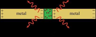
7 Electrically-injected III-V antenna-led 50nm interconnect nanoled ridge Ag Ag n-inp InGaAs(P) - Cavity-backed slot antenna 250nm p-inp + Electrical injection is straight forward Directional light emission for coupling into waveguide > 100 GHz direct modulation rate Page 7


8 Antenna-enhanced electroluminescence ~100-fold increase in spontaneous emission rate III-V No antenna III-V No antenna Antenna-LED Quantum efficiency τ nr τ rad Page 8


9 Increase QE 200-fold enhancement of spontaneous emission rate III-V 6nm InGaAs multiple quantum wells Page 9

10 Time-resolved light emission III-V No antenna III-V Antenna-LED Page 10
 Radiative recombination (kt current) Efficient")
11 High efficiency despite high surface recomb. velocity III-V n p InGaAs active region SRV = 10 4 cm/s Vf = 0.75 V Surface Injected current Surface recombination (2kT current) Radiative recombination (kt current) Efficient Page 11


12 Process induced surface damage Time-resolved photoluminescence Surface needs to be protected during fabrication! Page 12


13 Improved process with ultra-clean surface 1 Dry etch ridge Time-resolved photoluminescence 2 Deposit sacrificial Al 2 O 3 (expose to plasma, anneal, etc.) 3 Strip sacrificial Al 2 O 3 (TMAH) 11/8/2017 Page 13


14 Efficient waveguide Coupling Waveguide coupling efficiency Perspective view of the parabolic reflector Cross-section of simulated power flow Acknowledgement: Nicolas Andrade (UC Berkeley) Page 14
15 Summary Demonstrated 200-fold enhancement of spontaneous emission rate of electrically injected nanoscale III-V LED High efficiency possible despite large surface recombination velocity of III-V surface Ultra-clean InGaAs surface using sacrificial Al 2 O 3 Efficient and broadband coupling to single-mode on-chip waveguide is possible. 11/8/2017 Page 15


")
 Technical support")
16 Financial support Acknowledgments NSF Science and Technology Center for Energy Efficient Electronics Science (E 3 S) Air Force Office of Scientific Research (AFOSR) Berkeley Sensor & Actuator Center (BSAC) Technical support UC Berkeley Marvell Nanolab staff
17 Backup 11/8/ Fall Retreat Page 17


18 Electrically-injected III-V antenna-led Dielectric filled cavity Cavity-backed slot antenna III-V pn junction - + n p Far-field radiation Far-field radiation Page 18


19 Antenna mode Top view Advantages: Electrical injection is straight forward Self-aligned Directional light emission Thermal heat-sink 11/8/2017 Page 19

20 Spontaneous emission enhancement measurement Antenna enhancement directly increases quantum efficiency Injected carriers Radiative Nonradiative 11/8/2017 Page 20

21 Can radiative recombination ever exceed non-radiative recombination? 20nm I nr Injected current III-V Radiative Nonradiative


22 Electroluminescence measurement Optical image (frontside) Antenna-LED Measurement setup Semiconductor parameter analyzer i f ~1μA Antenna-LED chip n-contact Electroluminescence p-contact Microscope objective n-contact Spectrograph/ IR camera 35 μm Polarizer Lens

 Multiple quantum")

23 Toward >100 GHz direct modulation rate at high efficiency Theoretical 3dB frequency and efficiency Efficiency MOCVD growth by Fitzgerald group (MIT) Multiple quantum well (MQW) active region Doped active region and cladding layers Highly doped n-contact layer

24 Electrically-injected III-V antenna-led Top view Advantages: Electrical injection is straight forward Self-aligned fabrication Directional light emission for coupling into waveguide > 100 GHz direct modulation rate Cut-away drawing 11/8/2017 Page 24
Waveguide-Integrated Optical Antenna nanoleds for On-Chip Communication
 Waveguide-Integrated Optical Antenna nanoleds for On-Chip Communication Michael Eggleston, Kevin Messer, Seth Fortuna, Eli Yablonovitch, Ming C. Wu Department of Electrical Engineering and Computer Sciences
Spontaneous Hyper Emission: Title of Talk
 Spontaneous Hyper Emission: Title of Talk Enhanced Light Emission by Optical Antennas Ming C. Wu University of California, Berkeley A Science & Technology Center Where Our Paths Crossed Page Nanopatch
Integrated Nanoscale Antenna-LED for On-Chip Optical Communication
 Integrated Nanoscale Antenna-LED for On-Chip Optical Communication Seth Fortuna Electrical Engineering and Computer Sciences University of California at Berkeley Technical Report No. UCB/EECS-2017-144
Examination Optoelectronic Communication Technology. April 11, Name: Student ID number: OCT1 1: OCT 2: OCT 3: OCT 4: Total: Grade:
 Examination Optoelectronic Communication Technology April, 26 Name: Student ID number: OCT : OCT 2: OCT 3: OCT 4: Total: Grade: Declaration of Consent I hereby agree to have my exam results published on
Semiconductor Lasers Semiconductors were originally pumped by lasers or e-beams First diode types developed in 1962: Create a pn junction in
 Semiconductor Lasers Semiconductors were originally pumped by lasers or e-beams First diode types developed in 1962: Create a pn junction in semiconductor material Pumped now with high current density
InP-based Waveguide Photodetector with Integrated Photon Multiplication
 InP-based Waveguide Photodetector with Integrated Photon Multiplication D.Pasquariello,J.Piprek,D.Lasaosa,andJ.E.Bowers Electrical and Computer Engineering Department University of California, Santa Barbara,
Semiconductor Lasers Semiconductors were originally pumped by lasers or e-beams First diode types developed in 1962: Create a pn junction in
 Semiconductor Lasers Semiconductors were originally pumped by lasers or e-beams First diode types developed in 1962: Create a pn junction in semiconductor material Pumped now with high current density
Chapter 3 OPTICAL SOURCES AND DETECTORS
 Chapter 3 OPTICAL SOURCES AND DETECTORS 3. Optical sources and Detectors 3.1 Introduction: The success of light wave communications and optical fiber sensors is due to the result of two technological breakthroughs.
InP-based Waveguide Photodetector with Integrated Photon Multiplication
 InP-based Waveguide Photodetector with Integrated Photon Multiplication D.Pasquariello,J.Piprek,D.Lasaosa,andJ.E.Bowers Electrical and Computer Engineering Department University of California, Santa Barbara,
Light Sources, Modulation, Transmitters and Receivers
 Optical Fibres and Telecommunications Light Sources, Modulation, Transmitters and Receivers Introduction Previous section looked at Fibres. How is light generated in the first place? How is light modulated?
Lecture: Integration of silicon photonics with electronics. Prepared by Jean-Marc FEDELI CEA-LETI
 Lecture: Integration of silicon photonics with electronics Prepared by Jean-Marc FEDELI CEA-LETI Context The goal is to give optical functionalities to electronics integrated circuit (EIC) The objectives
Lecture 6 Fiber Optical Communication Lecture 6, Slide 1
 Lecture 6 Optical transmitters Photon processes in light matter interaction Lasers Lasing conditions The rate equations CW operation Modulation response Noise Light emitting diodes (LED) Power Modulation
Functional Materials. Optoelectronic devices
 Functional Materials Lecture 2: Optoelectronic materials and devices (inorganic). Photonic materials Optoelectronic devices Light-emitting diode (LED) displays Photodiode and Solar cell Photoconductive
Basic concepts. Optical Sources (b) Optical Sources (a) Requirements for light sources (b) Requirements for light sources (a)
 Optical Sources (a) Requirements for light sources (b) Requirements for light sources (a)") Optical Sources (a) Optical Sources (b) The main light sources used with fibre optic systems are: Light-emitting diodes (LEDs) Semiconductor lasers (diode lasers) Fibre laser and other compact solid-state
Optical Sources (a) Optical Sources (b) The main light sources used with fibre optic systems are: Light-emitting diodes (LEDs) Semiconductor lasers (diode lasers) Fibre laser and other compact solid-state
HIGH-EFFICIENCY MQW ELECTROABSORPTION MODULATORS
 HIGH-EFFICIENCY MQW ELECTROABSORPTION MODULATORS J. Piprek, Y.-J. Chiu, S.-Z. Zhang (1), J. E. Bowers, C. Prott (2), and H. Hillmer (2) University of California, ECE Department, Santa Barbara, CA 93106
Lecture 18: Photodetectors
 Lecture 18: Photodetectors Contents 1 Introduction 1 2 Photodetector principle 2 3 Photoconductor 4 4 Photodiodes 6 4.1 Heterojunction photodiode.................... 8 4.2 Metal-semiconductor photodiode................
Impact of the light coupling on the sensing properties of photonic crystal cavity modes Kumar Saurav* a,b, Nicolas Le Thomas a,b,
 Impact of the light coupling on the sensing properties of photonic crystal cavity modes Kumar Saurav* a,b, Nicolas Le Thomas a,b, a Photonics Research Group, Ghent University-imec, Technologiepark-Zwijnaarde
Micro-sensors - what happens when you make "classical" devices "small": MEMS devices and integrated bolometric IR detectors
 Micro-sensors - what happens when you make "classical" devices "small": MEMS devices and integrated bolometric IR detectors Dean P. Neikirk 1 MURI bio-ir sensors kick-off 6/16/98 Where are the targets
Optical MEMS in Compound Semiconductors Advanced Engineering Materials, Cal Poly, SLO November 16, 2007
 Optical MEMS in Compound Semiconductors Advanced Engineering Materials, Cal Poly, SLO November 16, 2007 Outline Brief Motivation Optical Processes in Semiconductors Reflectors and Optical Cavities Diode
Optical Fiber Communication Lecture 11 Detectors
 Optical Fiber Communication Lecture 11 Detectors Warriors of the Net Detector Technologies MSM (Metal Semiconductor Metal) PIN Layer Structure Semiinsulating GaAs Contact InGaAsP p 5x10 18 Absorption InGaAs
Optodevice Data Book ODE I. Rev.9 Mar Opnext Japan, Inc.
 Optodevice Data Book ODE-408-001I Rev.9 Mar. 2003 Opnext Japan, Inc. Section 1 Operating Principles 1.1 Operating Principles of Laser Diodes (LDs) and Infrared Emitting Diodes (IREDs) 1.1.1 Emitting Principles
Supplementary Note 1: Modeling of grating coupler
 Supplementary Note 1: Modeling of grating coupler For characterization purposes, the nanopillar LED is connected to a grating coupler by means of an adiabatic taper. The grating coupler was modeled with
Introduction Fundamentals of laser Types of lasers Semiconductor lasers
 ECE 5368 Introduction Fundamentals of laser Types of lasers Semiconductor lasers Introduction Fundamentals of laser Types of lasers Semiconductor lasers How many types of lasers? Many many depending on
Ultrafast direct modulation of a single-mode photonic crystal nanocavity light-emitting diode
 Received 8 Jun 211 Accepted 12 Oct 211 Published 15 Nov 211 DOI: 1.138/ncomms1543 Ultrafast direct modulation of a single-mode photonic crystal nanocavity light-emitting diode Gary Shambat 1, Bryan Ellis
Multi-GHz Operation of Tilted- Charge LED for Optical Interconnect
 Multi-GHz Operation of Tilted- Charge LED for Optical Interconnect Chao-Hsin Wu 吳肇欣 Department of Electrical Engineering & Graduate Institute of Photonics and Optoelectronics & Graduate Institute of Electronics
Graphene electro-optic modulator with 30 GHz bandwidth
 Graphene electro-optic modulator with 30 GHz bandwidth Christopher T. Phare 1, Yoon-Ho Daniel Lee 1, Jaime Cardenas 1, and Michal Lipson 1,2,* 1School of Electrical and Computer Engineering, Cornell University,
Optical Antenna Enhanced Spontaneous Emission in Semiconductors
 Optical Antenna Enhanced Spontaneous Emission in Semiconductors Kevin Messer Electrical Engineering and Computer Sciences University of California at Berkeley Technical Report No. UCB/EECS-2016-72 http://www.eecs.berkeley.edu/pubs/techrpts/2016/eecs-2016-72.html
Luminous Equivalent of Radiation
 Intensity vs λ Luminous Equivalent of Radiation When the spectral power (p(λ) for GaP-ZnO diode has a peak at 0.69µm) is combined with the eye-sensitivity curve a peak response at 0.65µm is obtained with
FABRICATION AND CHARACTERIZATION OF RESONANT CAVITY LIGHT-EMITTING TRANSISTORS MICHAEL E. LIU THESIS
 FABRICATION AND CHARACTERIZATION OF RESONANT CAVITY LIGHT-EMITTING TRANSISTORS BY MICHAEL E. LIU THESIS Submitted in partial fulfillment of the requirements for the degree of Master of Science in Electrical
Selectively-undercut traveling-wave electroabsorption modulators incorporating a p-ingaas contact layer
 Selectively-undercut traveling-wave electroabsorption modulators incorporating a p-ingaas contact layer Matthew M. Dummer, James R. Raring, Jonathan Klamkin, Anna Tauke-Pedretti, and Larry A. Coldren University
Integration of Optoelectronic and RF Devices for Applications in Optical Interconnect and Wireless Communication
 Integration of Optoelectronic and RF Devices for Applications in Optical Interconnect and Wireless Communication Zhaoran (Rena) Huang Assistant Professor Department of Electrical, Computer and System Engineering
Lecture 4 INTEGRATED PHOTONICS
 Lecture 4 INTEGRATED PHOTONICS What is photonics? Photonic applications use the photon in the same way that electronic applications use the electron. Devices that run on light have a number of advantages
VERTICAL CAVITY SURFACE EMITTING LASER
 VERTICAL CAVITY SURFACE EMITTING LASER Nandhavel International University Bremen 1/14 Outline Laser action, optical cavity (Fabry Perot, DBR and DBF) What is VCSEL? How does VCSEL work? How is it different
ECE 340 Lecture 29 : LEDs and Lasers Class Outline:
 ECE 340 Lecture 29 : LEDs and Lasers Class Outline: Light Emitting Diodes Lasers Semiconductor Lasers Things you should know when you leave Key Questions What is an LED and how does it work? How does a
Vertical External Cavity Surface Emitting Laser
 Chapter 4 Optical-pumped Vertical External Cavity Surface Emitting Laser The booming laser techniques named VECSEL combine the flexibility of semiconductor band structure and advantages of solid-state
Fabrication of antenna integrated UTC-PDs as THz sources
 Invited paper Fabrication of antenna integrated UTC-PDs as THz sources Siwei Sun 1, Tengyun Wang, Xiao xie 1, Lichen Zhang 1, Yuan Yao and Song Liang 1* 1 Key Laboratory of Semiconductor Materials Science,
Key Questions. What is an LED and how does it work? How does a laser work? How does a semiconductor laser work? ECE 340 Lecture 29 : LEDs and Lasers
 Things you should know when you leave Key Questions ECE 340 Lecture 29 : LEDs and Class Outline: What is an LED and how does it How does a laser How does a semiconductor laser How do light emitting diodes
Low Loss Waveguide Technologies & Purcell-Enhanced Emission
 MIT Microphotonics Center Fall Meeting, Boston, October 11, 2011 Low Loss Waveguide Technologies & Purcell-Enhanced Emission R. Tummidi, R. Pafchek, J. Li, G. Sukumaran, K. Kim, T. L. Koch Lehigh University
Design and fabrication of indium phosphide air-bridge waveguides with MEMS functionality
 Design and fabrication of indium phosphide air-bridge waveguides with MEMS functionality Wing H. Ng* a, Nina Podoliak b, Peter Horak b, Jiang Wu a, Huiyun Liu a, William J. Stewart b, and Anthony J. Kenyon
LEDs, Photodetectors and Solar Cells
 LEDs, Photodetectors and Solar Cells Chapter 7 (Parker) ELEC 424 John Peeples Why the Interest in Photons? Answer: Momentum and Radiation High electrical current density destroys minute polysilicon and
Optical Interconnection in Silicon LSI
 The Fifth Workshop on Nanoelectronics for Tera-bit Information Processing, 1 st Century COE, Hiroshima University Optical Interconnection in Silicon LSI Shin Yokoyama, Yuichiro Tanushi, and Masato Suzuki
Metal Optics Based nanoleds: In Search of a Fast, Efficient, Nanoscale Light Emitter
 Metal Optics Based nanoleds: In Search of a Fast, Efficient, Nanoscale Light Emitter Michael Eggleston Electrical Engineering and Computer Sciences University of California at Berkeley Technical Report
Robert G. Hunsperger. Integrated Optics. Theory and Technology. Sixth Edition. 4ü Spri rineer g<
 Robert G. Hunsperger Integrated Optics Theory and Technology Sixth Edition 4ü Spri rineer g< 1 Introduction 1 1.1 Advantages of Integrated Optics 2 1.1.1 Comparison of Optical Fibers with Other Interconnectors
High-speed Ge photodetector monolithically integrated with large cross silicon-on-insulator waveguide
 [ APPLIED PHYSICS LETTERS ] High-speed Ge photodetector monolithically integrated with large cross silicon-on-insulator waveguide Dazeng Feng, Shirong Liao, Roshanak Shafiiha. etc Contents 1. Introduction
Nd:YSO resonator array Transmission spectrum (a. u.) Supplementary Figure 1. An array of nano-beam resonators fabricated in Nd:YSO.
 Supplementary Figure 1. An array of nano-beam resonators fabricated in Nd:YSO.") a Nd:YSO resonator array µm Transmission spectrum (a. u.) b 4 F3/2-4I9/2 25 2 5 5 875 88 λ(nm) 885 Supplementary Figure. An array of nano-beam resonators fabricated in Nd:YSO. (a) Scanning electron microscope
a Nd:YSO resonator array µm Transmission spectrum (a. u.) b 4 F3/2-4I9/2 25 2 5 5 875 88 λ(nm) 885 Supplementary Figure. An array of nano-beam resonators fabricated in Nd:YSO. (a) Scanning electron microscope
Si CMOS Technical Working Group
 Si CMOS Technical Working Group CTR, Spring 2008 meeting Markets Interconnects TWG Breakouts Reception TWG reports Si CMOS: photonic integration E-P synergy - Integration - Standardization - Cross-market
Intersubband spectroscopy of electron tunneling in GaN/AlN coupled quantum wells
 Intersubband spectroscopy of electron tunneling in GaN/AlN coupled quantum wells N. Kheirodin, L. Nevou, M. Tchernycheva, F. H. Julien, A. Lupu, P. Crozat, L. Meignien, E. Warde, L.Vivien Institut d Electronique
RECENTLY, using near-field scanning optical
 1 2 1 2 Theoretical and Experimental Study of Near-Field Beam Properties of High Power Laser Diodes W. D. Herzog, G. Ulu, B. B. Goldberg, and G. H. Vander Rhodes, M. S. Ünlü L. Brovelli, C. Harder Abstract
Segmented waveguide photodetector with 90% quantum efficiency
 Vol. 26, No. 10 14 May 2018 OPTICS EXPRESS 12499 Segmented waveguide photodetector with 90% quantum efficiency QIANHUAN YU, KEYE SUN, QINGLONG LI, AND ANDREAS BELING* Department of Electrical and Computer
The Past, Present, and Future of Silicon Photonics
 The Past, Present, and Future of Silicon Photonics Myung-Jae Lee High-Speed Circuits & Systems Lab. Dept. of Electrical and Electronic Engineering Yonsei University Outline Introduction A glance at history
Ultra-low voltage resonant tunnelling diode electroabsorption modulator
 Ultra-low voltage resonant tunnelling diode electroabsorption modulator, 1/10 Ultra-low voltage resonant tunnelling diode electroabsorption modulator J. M. L. FIGUEIREDO Faculdade de Ciências e Tecnologia,
Nanophotonics: Single-nanowire electrically driven lasers
 Nanophotonics: Single-nanowire electrically driven lasers Ivan Stepanov June 19, 2010 Single crystaline nanowires have unique optic and electronic properties and their potential use in novel photonic and
SUPPLEMENTARY INFORMATION
 Room-temperature continuous-wave electrically injected InGaN-based laser directly grown on Si Authors: Yi Sun 1,2, Kun Zhou 1, Qian Sun 1 *, Jianping Liu 1, Meixin Feng 1, Zengcheng Li 1, Yu Zhou 1, Liqun
Lecture 8 Optical Sensing. ECE 5900/6900 Fundamentals of Sensor Design
 ECE 5900/6900: Fundamentals of Sensor Design Lecture 8 Optical Sensing 1 Optical Sensing Q: What are we measuring? A: Electromagnetic radiation labeled as Ultraviolet (UV), visible, or near,mid-, far-infrared
LAB V. LIGHT EMITTING DIODES
 LAB V. LIGHT EMITTING DIODES 1. OBJECTIVE In this lab you are to measure I-V characteristics of Infrared (IR), Red and Blue light emitting diodes (LEDs). The emission intensity as a function of the diode
PHYSICAL ELECTRONICS(ECE3540) APPLICATIONS OF PHYSICAL ELECTRONICS PART I
 APPLICATIONS OF PHYSICAL ELECTRONICS PART I") PHYSICAL ELECTRONICS(ECE3540) APPLICATIONS OF PHYSICAL ELECTRONICS PART I Tennessee Technological University Monday, October 28, 2013 1 Introduction In the following slides, we will discuss the summary
PHYSICAL ELECTRONICS(ECE3540) APPLICATIONS OF PHYSICAL ELECTRONICS PART I Tennessee Technological University Monday, October 28, 2013 1 Introduction In the following slides, we will discuss the summary
64 Channel Flip-Chip Mounted Selectively Oxidized GaAs VCSEL Array
 64 Channel Flip-Chip Mounted Selectively Oxidized GaAs VCSEL Array 69 64 Channel Flip-Chip Mounted Selectively Oxidized GaAs VCSEL Array Roland Jäger and Christian Jung We have designed and fabricated
Semiconductor Optical Communication Components and Devices Lecture 18: Introduction to Diode Lasers - I
 Semiconductor Optical Communication Components and Devices Lecture 18: Introduction to Diode Lasers - I Prof. Utpal Das Professor, Department of lectrical ngineering, Laser Technology Program, Indian Institute
Vertical-cavity surface-emitting lasers (VCSELs)
") 78 Technology focus: Lasers Advancing InGaN VCSELs Mike Cooke reports on progress towards filling the green gap and improving tunnel junctions as alternatives to indium tin oxide current-spreading layers.
78 Technology focus: Lasers Advancing InGaN VCSELs Mike Cooke reports on progress towards filling the green gap and improving tunnel junctions as alternatives to indium tin oxide current-spreading layers.
High-Speed Opto-Electronic Components for Digital and Analog RF Systems
 High-Speed Opto-Electronic Components for Digital and Analog RF Systems K. Y. Liou Director Laser Technology & Government Business Multiplex, Inc. kyliou@multiplexinc.com WOCC April 23, 2005 5000 Hadley
Application Instruction 002. Superluminescent Light Emitting Diodes: Device Fundamentals and Reliability
 I. Introduction II. III. IV. SLED Fundamentals SLED Temperature Performance SLED and Optical Feedback V. Operation Stability, Reliability and Life VI. Summary InPhenix, Inc., 25 N. Mines Road, Livermore,
Design and Simulation of N-Substrate Reverse Type Ingaasp/Inp Avalanche Photodiode
 International Refereed Journal of Engineering and Science (IRJES) ISSN (Online) 2319-183X, (Print) 2319-1821 Volume 2, Issue 8 (August 2013), PP.34-39 Design and Simulation of N-Substrate Reverse Type
Ultra-low power fiber-coupled gallium arsenide photonic crystal cavity electro-optic modulator
 Ultra-low power fiber-coupled gallium arsenide photonic crystal cavity electro-optic modulator Gary Shambat, 1,* Bryan Ellis, 1 Marie A. Mayer, 2 Arka Majumdar, 1 Eugene E. Haller, 2 and Jelena Vučković
Novel cascaded injection-locked 1.55-µm VCSELs with 66 GHz modulation bandwidth
 Novel cascaded injection-locked 1.55-µm VCSELs with 66 GHz modulation bandwidth Xiaoxue Zhao, 1 * Devang Parekh, 1 Erwin K. Lau, 1 Hyuk-Kee Sung, 1, 3 Ming C. Wu, 1 Werner Hofmann, 2 Markus C. Amann, 2
LAB V. LIGHT EMITTING DIODES
 LAB V. LIGHT EMITTING DIODES 1. OBJECTIVE In this lab you will measure the I-V characteristics of Infrared (IR), Red and Blue light emitting diodes (LEDs). Using a photodetector, the emission intensity
CHAPTER 6 CARBON NANOTUBE AND ITS RF APPLICATION
 CHAPTER 6 CARBON NANOTUBE AND ITS RF APPLICATION 6.1 Introduction In this chapter we have made a theoretical study about carbon nanotubes electrical properties and their utility in antenna applications.
Laser Diode. Photonic Network By Dr. M H Zaidi
 Laser Diode Light emitters are a key element in any fiber optic system. This component converts the electrical signal into a corresponding light signal that can be injected into the fiber. The light emitter
Lecture 4 Fiber Optical Communication Lecture 4, Slide 1
 Lecture 4 Optical transmitters Photon processes in light matter interaction Lasers Lasing conditions The rate equations CW operation Modulation response Noise Light emitting diodes (LED) Power Modulation
Optoelectronic integrated circuits incorporating negative differential resistance devices
 Optoelectronic integrated circuits incorporating negative differential resistance devices José Figueiredo Centro de Electrónica, Optoelectrónica e Telecomunicações Departamento de Física da Faculdade de
Design of External Cavity Semiconductor Lasers to Suppress Wavelength Shift and Mode Hopping
 ST/03/055/PM Design o External Cavity Semiconductor Lasers to Suppress Wavelength Shit and Mode Hopping L. Zhao and Z. P. Fang Abstract In this report, a model o ernal cavity semiconductor laser is built,
rd IEEE International Semiconductor Laser Conference (ISLC 2012) San Diego, California, USA 7 10 October IEEE Catalog Number: ISBN:
 San Diego, California, USA 7 10 October IEEE Catalog Number: ISBN:") 2012 23rd IEEE International Semiconductor Laser Conference (ISLC 2012) San Diego, California, USA 7 10 October 2012 IEEE Catalog Number: ISBN: CFP12SLC-PRT 978-1-4577-0828-2 Monday, October 8, 2012 PLE
2012 23rd IEEE International Semiconductor Laser Conference (ISLC 2012) San Diego, California, USA 7 10 October 2012 IEEE Catalog Number: ISBN: CFP12SLC-PRT 978-1-4577-0828-2 Monday, October 8, 2012 PLE
Monolithically integrated InGaAs nanowires on 3D. structured silicon-on-insulator as a new platform for. full optical links
 Monolithically integrated InGaAs nanowires on 3D structured silicon-on-insulator as a new platform for full optical links Hyunseok Kim 1, Alan C. Farrell 1, Pradeep Senanayake 1, Wook-Jae Lee 1,* & Diana.
MICRO RING MODULATOR. Dae-hyun Kwon. High-speed circuits and Systems Laboratory
 MICRO RING MODULATOR Dae-hyun Kwon High-speed circuits and Systems Laboratory Paper preview Title of the paper Low Vpp, ultralow-energy, compact, high-speed silicon electro-optic modulator Publication
Wavelength-independent coupler from fiber to an on-chip cavity, demonstrated over an 850nm span. Steven Wang, Tal Carmon, Eric Ostby and Kerry Vahala
 Wavelength-independent coupler from fiber to an on-chip, demonstrated over an 85nm span Steven Wang, Tal Carmon, Eric Ostby and Kerry Vahala Basics of coupling Importance of phase match ( λ ) 1 ( λ ) 2
Comparison of FMCW-LiDAR system with optical- and electricaldomain swept light sources toward self-driving mobility application
 P1 Napat J.Jitcharoenchai Comparison of FMCW-LiDAR system with optical- and electricaldomain swept light sources toward self-driving mobility application Napat J.Jitcharoenchai, Nobuhiko Nishiyama, Tomohiro
Optical Transmission Fundamentals
 Optical Transmission Fundamentals F. Vasey, CERN-EP-ESE Context Technology HEP Specifics 12 Nov 2018 0 Context: Bandwidth Demand Internet traffic is growing at ~Moore s law Global interconnection bandwidth
Advanced semiconductor lasers
 Advanced semiconductor lasers Quantum cascade lasers Single mode lasers DFBs, VCSELs, etc. Quantum cascade laser Reminder: Semiconductor laser diodes Conventional semiconductor laser CB diode laser: material
Electronic-Photonic ICs for Low Cost and Scalable Datacenter Solutions
 Electronic-Photonic ICs for Low Cost and Scalable Datacenter Solutions Christoph Theiss, Director Packaging Christoph.Theiss@sicoya.com 1 SEMICON Europe 2016, October 27 2016 Sicoya Overview Spin-off from
Physics of Waveguide Photodetectors with Integrated Amplification
 Physics of Waveguide Photodetectors with Integrated Amplification J. Piprek, D. Lasaosa, D. Pasquariello, and J. E. Bowers Electrical and Computer Engineering Department University of California, Santa
Silicon-based photonic crystal nanocavity light emitters
 Silicon-based photonic crystal nanocavity light emitters Maria Makarova, Jelena Vuckovic, Hiroyuki Sanda, Yoshio Nishi Department of Electrical Engineering, Stanford University, Stanford, CA 94305-4088
Degradation analysis in asymmetric sampled grating distributed feedback laser diodes
 Microelectronics Journal 8 (7) 74 74 www.elsevier.com/locate/mejo Degradation analysis in asymmetric sampled grating distributed feedback laser diodes Han Sung Joo, Sang-Wan Ryu, Jeha Kim, Ilgu Yun Semiconductor
Supporting Information for Gbps terahertz external. modulator based on a composite metamaterial with a. double-channel heterostructure
 Supporting Information for Gbps terahertz external modulator based on a composite metamaterial with a double-channel heterostructure Yaxin Zhang, Shen Qiao*, Shixiong Liang, Zhenhua Wu, Ziqiang Yang*,
Heinrich-Hertz-Institut Berlin
 NOVEMBER 24-26, ECOLE POLYTECHNIQUE, PALAISEAU OPTICAL COUPLING OF SOI WAVEGUIDES AND III-V PHOTODETECTORS Ludwig Moerl Heinrich-Hertz-Institut Berlin Photonic Components Dept. Institute for Telecommunications,,
Investigate the characteristics of PIN Photodiodes and understand the usage of the Lightwave Analyzer component.
 PIN Photodiode 1 OBJECTIVE Investigate the characteristics of PIN Photodiodes and understand the usage of the Lightwave Analyzer component. 2 PRE-LAB In a similar way photons can be generated in a semiconductor,
Photomixer as a self-oscillating mixer
 Photomixer as a self-oscillating mixer Shuji Matsuura The Institute of Space and Astronautical Sciences, 3-1-1 Yoshinodai, Sagamihara, Kanagawa 9-8510, Japan. e-mail:matsuura@ir.isas.ac.jp Abstract Photomixing
Instruction manual and data sheet ipca h
 1/15 instruction manual ipca-21-05-1000-800-h Instruction manual and data sheet ipca-21-05-1000-800-h Broad area interdigital photoconductive THz antenna with microlens array and hyperhemispherical silicon
Components of Optical Instruments 1
 Components of Optical Instruments 1 Optical phenomena used for spectroscopic methods: (1) absorption (2) fluorescence (3) phosphorescence (4) scattering (5) emission (6) chemiluminescence Spectroscopic
MAJOR REQUIREMENTS OPTICAL FIBER EMITTER
 MAJOR REQUIREMENTS OPTICAL FIBER EMITTER 1. LIGHT 0/P SHOULD BE HIGHLY DIRECTIONAL. 2. SOURCE SHOULD BE LINEAR (MIN. DISTORTION AND NOISE) 3. SHOULD EMIT LIGHT AT WAVELENGTHS WHERE THE FIBER HAS LOW LOSSES
Optical Amplifiers Photonics and Integrated Optics (ELEC-E3240) Zhipei Sun Photonics Group Department of Micro- and Nanosciences Aalto University
 Zhipei Sun Photonics Group Department of Micro- and Nanosciences Aalto University") Photonics Group Department of Micro- and Nanosciences Aalto University Optical Amplifiers Photonics and Integrated Optics (ELEC-E3240) Zhipei Sun Last Lecture Topics Course introduction Ray optics & optical
Photonics Group Department of Micro- and Nanosciences Aalto University Optical Amplifiers Photonics and Integrated Optics (ELEC-E3240) Zhipei Sun Last Lecture Topics Course introduction Ray optics & optical
Design of InGaAs/InP 1.55μm vertical cavity surface emitting lasers (VCSEL)
") Design of InGaAs/InP 1.55μm vertical cavity surface emitting lasers (VCSEL) J.-M. Lamy, S. Boyer-Richard, C. Levallois, C. Paranthoën, H. Folliot, N. Chevalier, A. Le Corre, S. Loualiche UMR FOTON 6082
Design of InGaAs/InP 1.55μm vertical cavity surface emitting lasers (VCSEL) J.-M. Lamy, S. Boyer-Richard, C. Levallois, C. Paranthoën, H. Folliot, N. Chevalier, A. Le Corre, S. Loualiche UMR FOTON 6082
Optical Communication and Networks M.N. Bandyopadhyay
 Optical Communication and Networks M.N. Bandyopadhyay Director National Institute of Technology (NIT) Calicut Delhi-110092 2014 OPTICAL COMMUNICATION AND NETWORKS M.N. Bandyopadhyay 2014 by PHI Learning
Modulating Retro-reflector Links for High Bandwidth Free-Space Lasercomm. Dr. William Rabinovich US Naval Research Laboratory,
 Modulating Retro-reflector Links for High Bandwidth Free-Space Lasercomm Dr. William Rabinovich US Naval Research Laboratory, MRRs in ONR BAA 09-18 Product 2 Modulating retro-reflector (MRR) communications
CONTENTS. 2.2 Schrodinger's Wave Equation 31. PART I Semiconductor Material Properties. 2.3 Applications of Schrodinger's Wave Equation 34
 CONTENTS Preface x Prologue Semiconductors and the Integrated Circuit xvii PART I Semiconductor Material Properties CHAPTER 1 The Crystal Structure of Solids 1 1.0 Preview 1 1.1 Semiconductor Materials
Ph 77 ADVANCED PHYSICS LABORATORY ATOMIC AND OPTICAL PHYSICS
 Ph 77 ADVANCED PHYSICS LABORATORY ATOMIC AND OPTICAL PHYSICS Diode Laser Characteristics I. BACKGROUND Beginning in the mid 1960 s, before the development of semiconductor diode lasers, physicists mostly
The Light at the End of the Wire. Dana Vantrease + HP Labs + Mikko Lipasti
 The Light at the End of the Wire Dana Vantrease + HP Labs + Mikko Lipasti 1 Goals of This Talk Why should we (architects) be interested in optics? How does on-chip optics work? What can we build with optics?
Si and InP Integration in the HELIOS project
 Si and InP Integration in the HELIOS project J.M. Fedeli CEA-LETI, Grenoble ( France) ECOC 2009 1 Basic information about HELIOS HELIOS photonics ELectronics functional Integration on CMOS www.helios-project.eu
Record Extrinsic Transconductance (2.45 ms/μm at V DS = 0.5 V) InAs/In 0.53 Ga 0.47 As Channel MOSFETs Using MOCVD Source-Drain Regrowth
 InAs/In 0.53 Ga 0.47 As Channel MOSFETs Using MOCVD Source-Drain Regrowth") Record Extrinsic Transconductance (2.45 ms/μm at = 0.5 V) InAs/In 0.53 Ga 7 As Channel MOSFETs Using MOCVD Source-Drain Regrowth Sanghoon Lee 1*, C.-Y. Huang 1, A. D. Carter 1, D. C. Elias 1, J. J. M.
Record Extrinsic Transconductance (2.45 ms/μm at = 0.5 V) InAs/In 0.53 Ga 7 As Channel MOSFETs Using MOCVD Source-Drain Regrowth Sanghoon Lee 1*, C.-Y. Huang 1, A. D. Carter 1, D. C. Elias 1, J. J. M.
Review of Semiconductor Physics
 Review of Semiconductor Physics k B 1.38 u 10 23 JK -1 a) Energy level diagrams showing the excitation of an electron from the valence band to the conduction band. The resultant free electron can freely
GaSb based high power single spatial mode and distributed feedback lasers at 2.0 μm
 GaSb based high power single spatial mode and distributed feedback lasers at 2.0 μm Clifford Frez 1, Kale J. Franz 1, Alexander Ksendzov, 1 Jianfeng Chen 2, Leon Sterengas 2, Gregory L. Belenky 2, Siamak
Deformable MEMS Micromirror Array for Wavelength and Angle Insensitive Retro-Reflecting Modulators Trevor K. Chan & Joseph E. Ford
 Photonics Systems Integration Lab UCSD Jacobs School of Engineering Deformable MEMS Micromirror Array for Wavelength and Angle Insensitive Retro-Reflecting Modulators Trevor K. Chan & Joseph E. Ford PHOTONIC