PHYSICAL ELECTRONICS(ECE3540) APPLICATIONS OF PHYSICAL ELECTRONICS PART I
|
|
|
- Myles Farmer
- 5 years ago
- Views:
Transcription


1 PHYSICAL ELECTRONICS(ECE3540) APPLICATIONS OF PHYSICAL ELECTRONICS PART I Tennessee Technological University Monday, October 28,
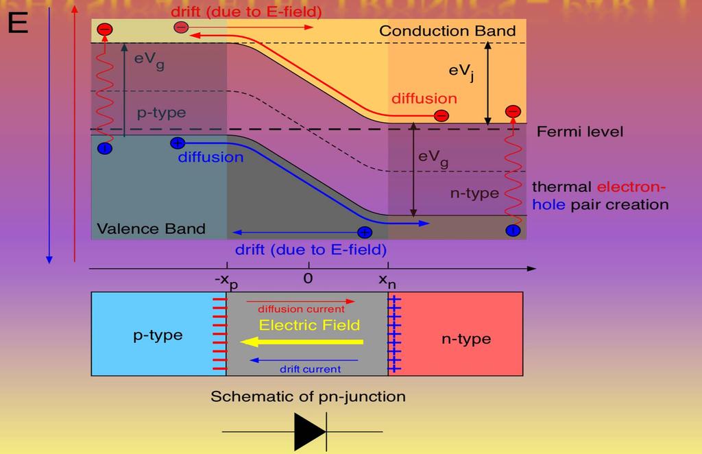
2 Introduction In the following slides, we will discuss the summary of the Reading Assignment: the concepts of a large reverse-bias voltage that cause a Junction Breakdown, thezener Effect and the Avalanche Effect. 1. Junction Breakdown, Avalanche Breakdown, Tunneling Breakdown 2. Zener Diodes 3. Tunnel Diodes 4. Applications of Physical Electronics I: PN Junction Diodes. More discussion on these concepts in Chapter 12. Tennessee Technological University Monday, October 28,
3 PHYSICAL ELECTRONICS(ECE3540) Explanation of the Reading Assignment Zener Diodes and Tunnel Diodes Tennessee Technological University Monday, October 28,
4 Junction Breakdown Filled States - Empty States E c E v Dominant if both sides of a junction are very heavily doped. Can be classified into two: 1. Zener Breakdown 2. Avalanche Breakdown I V E p E crit 10 6 V/cm Breakdown Tennessee Technological University Monday, October 28,
5 1. Zener Breakdown I V B, breakdown voltage Small leakage Current A Forward Current V R P N R A Zener diode B 3.7 V A Zener diode is designed to operate in the breakdown mode. C D IC Tennessee Technological University Monday, October 28,
6 Peak Electric Field Deletion layer N+ P N a Neutral Region increasing reverse bias E p E 0 x p (a) increasing reverse bias E p 2qN E( 0) ( bi Vr ) s 1/2 x p (b) x V B 2 secrit 2 qn bi Tennessee Technological University Monday, October 28,
7 E c E E Fp v electron-hole pair generation 2. Avalanche Breakdown Impact ionization: an energetic original electron electron generating electron and hole, which can also cause impact ionization. Impact ionization + positive feedbackavalanche breakdown V B secrit 2qN 2 E c E Fn V B 1 N 1 N a 1 N d E v Tennessee Technological University Monday, October 28,
8 Quantum Mechanical Tunneling Fig. 1 Quantum Mechanical Tunneling Tunneling probability: 2 ( 8 m P exp 2T ( V E ) 2 H h A tunnel diode or Esaki diode is a type of semiconductor that is capable of very fast operation, well into the microwave frequency region, made possible by the use of the quantum mechanical effect called tunneling. ) Tennessee Technological University Monday, October 28,
9 Tunnel Diode Under normal forward bias operation, as voltage begins to increase, electrons at first tunnel through the very narrow p n junction barrier because filled electron states in the conduction band on the n-side become aligned with empty valence band hole states on the p-side of the p-n junction. As voltage increases further these states become more misaligned and the current drops this is called negative resistance because current decreases with increasing voltage. As voltage increases yet further, the diode begins to operate as a normal diode. Tennessee Technological University Monday, October 28,
10 Tunnel Diode In the reverse direction, tunnel diodes are called back diodes (or backward diodes) andcan act as fast rectifiers with zero offset voltage and extreme linearity for power signals (they have an accurate square law characteristic in the reverse direction). Under reverse bias, filled states on the p-side become increasingly aligned with empty states on the n-side and electrons now tunnel through the PN junction barrier in reverse direction. Tennessee Technological University Monday, October 28,
11 Tunnel Diode Fig. 2: a) Simplified Energy band diagram of a tunnel diode with a reverse bias voltage b) I-V Characteristic of a Tunnel Diode with a reverse-bias voltage Tennessee Technological University Monday, October 28,

12 PHYSICAL ELECTRONICS(ECE3540) APPLICATIONS OF PN JUNCTION DIODES Tennessee Technological University Monday, October 28,
13 The PN Junction as a Temperature Sensor I qv kt I0( e 1) I 0 Aqn 2 i L D p p N d Dn L N n a Fig. 3: PN Junction diode as a Temperature Sensor What causes the IV curves to shift to lower V at higher T? Tennessee Technological University Monday, October 28,
14 Solar Cells Fig. 4: World Energy Consumption Solar Cells are also known as photovoltaic cells (PV). Convert sunlight to electricity with 10-30% conversion efficiency. 1 m 2 solar cell generate about 150 W peak or 25 W continuous power. Low cost and high efficiency are needed for wide deployment. Tennessee Technological University Monday, October 28,
15 Solar Cell Basics light N Short Circuit P I sc I Dark IV Eq.(4.9.4) V V E c Solar Cell IV E v + (a) I sc Maximum power-output I qv kt I ( 0 e 1) I sc Tennessee Technological University Monday, October 28,
16 Light Absorption Light intensity (x) α(1/cm): absorption coefficient e -x Fig. 5: Photon Energy vs. Absorption Coefficient hc Photon Energy (ev) 1.24 ( m) A thinner layer of direct-gap semiconductor can absorb most of solar radiation than indirect-gap semiconductor. Compare Si and Ge. Tennessee Technological University Monday, October 28,
17 Output Power A particular operating point on the solar cell I-V curve maximizes the output power (I x V). Output Power I sc V oc FF Si solar cell with 15-20% efficiency dominates the market now Theoretically, the highest efficiency (~24%) can be obtained with 1.9eV >E g >1.2eV. Larger E g lead to too low I sc (low light absorption); smaller E g leads to too low Voc. Tandem solar cells gets 35% efficiency using large and small E g materials tailored to the short and long wavelength solar light. Tennessee Technological University Monday, October 28,
18 Light Emitting Diodes and Solid-State Lighting Light emitting diodes (LEDs) LEDs are made of compound semiconductors such as InP and GaN. Light is emitted when electron and hole undergo radiative recombination. E c Radiative recombination E v Non-radiative recombination through traps Tennessee Technological University Monday, October 28,
19 LED Materials and Structure Fig. 7: LED Materials and Structure LED wavelength ( m) 1.24 photon energy 1.24 ( ev ) E g Tennessee Technological University Monday, October 28,
20 LED Materials and Structure E g (ev) Wavelength (μm) Color Lattice constant (Å) InAs InN infrared 3.45 InP GaAs red 5.66 yellow GaP blue 5.46 AlP violet 5.45 GaN AlN UV 3.11 Table: Light-emitting diode materials compound semiconductors binary semiconductors: - Ex: GaAs, efficient emitter ternary semiconductor : -Ex: GaAs 1-x P x, tunable E g (to vary the color) quaternary semiconductors: - Ex: AlInGaP, tunable E g and lattice constant (for growing high quality epitaxial films on inexpensive substrates) Tennessee Technological University Monday, October 28,

21 Common LEDs Spectral range Material System Substrate Example Applications Infrared InGaAsP InP Optical communication Infrared- Red GaAsP GaAs Indicator lamps. Remote control Red- Yellow AlInGaP GaA or GaP Optical communication. High-brightness traffic signal lights Green- Blue InGaN GaN or sapphire High brightness signal lights. Video billboards Blue-UV AlInGaN GaN or sapphire Solid-state lighting Red- Blue Organic semiconductors glass Displays Tennessee Technological University Monday, October 28,
22 Solid-State Lighting luminosity (lumen, lm): a measure of visible light energy normalized to the sensitivity of the human eye at different wavelengths Incandescent lamp Compact fluorescent lamp Tube fluorescent lamp White LED Theoretical limit at peak of eye sensitivity ( λ=555nm) Theoretical limit (white light) ~340 Luminous efficacy of lamps in lumen/watt Organic Light Emitting Diodes (OLED) : has lower efficacy than nitride or aluminide based compound semiconductor LEDs. Terms: luminosity measured in lumens, luminous efficacy Tennessee Technological University Monday, October 28,

23 (a) Absorption Diode Lasers Light Amplification (d) Net Light Absorption (b) Spontaneous Emission (c) Stimulated Emission (e) Net Light Amplification Light amplification requires population inversion: electron occupation probability is larger for higher E states than lower E states. Stimulated emission: emitted photon has identical frequency and directionality as the stimulating photon; light wave is amplified. Tennessee Technological University Monday, October 28,
24 Laser Applications Red diode lasers: CD, DVD reader/writer Blue diode lasers: Blu-ray DVD (higher storage density) 1.55 m infrared diode lasers: Fiber-optic communication Photodiodes Photodiodes: Reverse biased PN diode. Detects photo-generated current (similar to I sc of solar cell) for optical communication, DVD reader, etc. Avalanche photodiodes: Photodiodes operating near avalanche breakdown amplifies photocurrent by impact ionization. Tennessee Technological University Monday, October 28,
25 Picture Credits Semiconductor Physics and Devices, Donald Neaman, 4th Edition, McGraw Hill Publications. Modern Semiconductor Devices for Integrated Circuits, Prof. Chenming Calvin Hu, UC Berkeley. Tennessee Technological University Monday, October 28,
LEDs, Photodetectors and Solar Cells
 LEDs, Photodetectors and Solar Cells Chapter 7 (Parker) ELEC 424 John Peeples Why the Interest in Photons? Answer: Momentum and Radiation High electrical current density destroys minute polysilicon and
Functional Materials. Optoelectronic devices
 Functional Materials Lecture 2: Optoelectronic materials and devices (inorganic). Photonic materials Optoelectronic devices Light-emitting diode (LED) displays Photodiode and Solar cell Photoconductive
What is the highest efficiency Solar Cell?
 What is the highest efficiency Solar Cell? GT CRC Roof-Mounted PV System Largest single PV structure at the time of it s construction for the 1996 Olympic games Produced more than 1 billion watt hrs. of
ECE 340 Lecture 29 : LEDs and Lasers Class Outline:
 ECE 340 Lecture 29 : LEDs and Lasers Class Outline: Light Emitting Diodes Lasers Semiconductor Lasers Things you should know when you leave Key Questions What is an LED and how does it work? How does a
Key Questions. What is an LED and how does it work? How does a laser work? How does a semiconductor laser work? ECE 340 Lecture 29 : LEDs and Lasers
 Things you should know when you leave Key Questions ECE 340 Lecture 29 : LEDs and Class Outline: What is an LED and how does it How does a laser How does a semiconductor laser How do light emitting diodes
Diodes Rectifiers, Zener diodes light emitting diodes, laser diodes photodiodes, optocouplers
 Diodes Rectifiers, Zener diodes light emitting diodes, laser diodes photodiodes, optocouplers Prepared by Scott Robertson Fall 2007 Physics 3330 1 Impurity-doped semiconductors Semiconductors (Ge, Si)
Luminous Equivalent of Radiation
 Intensity vs λ Luminous Equivalent of Radiation When the spectral power (p(λ) for GaP-ZnO diode has a peak at 0.69µm) is combined with the eye-sensitivity curve a peak response at 0.65µm is obtained with
Photodiode: LECTURE-5
 LECTURE-5 Photodiode: Photodiode consists of an intrinsic semiconductor sandwiched between two heavily doped p-type and n-type semiconductors as shown in Fig. 3.2.2. Sufficient reverse voltage is applied
10/27/2009 Reading: Chapter 10 of Hambley Basic Device Physics Handout (optional)
") EE40 Lec 17 PN Junctions Prof. Nathan Cheung 10/27/2009 Reading: Chapter 10 of Hambley Basic Device Physics Handout (optional) Slide 1 PN Junctions Semiconductor Physics of pn junctions (for reference
EE40 Lec 17 PN Junctions Prof. Nathan Cheung 10/27/2009 Reading: Chapter 10 of Hambley Basic Device Physics Handout (optional) Slide 1 PN Junctions Semiconductor Physics of pn junctions (for reference
LAB V. LIGHT EMITTING DIODES
 LAB V. LIGHT EMITTING DIODES 1. OBJECTIVE In this lab you are to measure I-V characteristics of Infrared (IR), Red and Blue light emitting diodes (LEDs). The emission intensity as a function of the diode
Chapter 3 OPTICAL SOURCES AND DETECTORS
 Chapter 3 OPTICAL SOURCES AND DETECTORS 3. Optical sources and Detectors 3.1 Introduction: The success of light wave communications and optical fiber sensors is due to the result of two technological breakthroughs.
Lecture 18: Photodetectors
 Lecture 18: Photodetectors Contents 1 Introduction 1 2 Photodetector principle 2 3 Photoconductor 4 4 Photodiodes 6 4.1 Heterojunction photodiode.................... 8 4.2 Metal-semiconductor photodiode................
Design and Simulation of N-Substrate Reverse Type Ingaasp/Inp Avalanche Photodiode
 International Refereed Journal of Engineering and Science (IRJES) ISSN (Online) 2319-183X, (Print) 2319-1821 Volume 2, Issue 8 (August 2013), PP.34-39 Design and Simulation of N-Substrate Reverse Type
Introduction to Optoelectronic Devices
 Introduction to Optoelectronic Devices Dr. Jing Bai Assistant Professor Department of Electrical and Computer Engineering University of Minnesota Duluth October 30th, 2012 1 Outline What is the optoelectronics?
Semiconductor Lasers Semiconductors were originally pumped by lasers or e-beams First diode types developed in 1962: Create a pn junction in
 Semiconductor Lasers Semiconductors were originally pumped by lasers or e-beams First diode types developed in 1962: Create a pn junction in semiconductor material Pumped now with high current density
LAB V. LIGHT EMITTING DIODES
 LAB V. LIGHT EMITTING DIODES 1. OBJECTIVE In this lab you will measure the I-V characteristics of Infrared (IR), Red and Blue light emitting diodes (LEDs). Using a photodetector, the emission intensity
10/14/2009. Semiconductor basics pn junction Solar cell operation Design of silicon solar cell
 PHOTOVOLTAICS Fundamentals PV FUNDAMENTALS Semiconductor basics pn junction Solar cell operation Design of silicon solar cell SEMICONDUCTOR BASICS Allowed energy bands Valence and conduction band Fermi
Problem 4 Consider a GaAs p-n + junction LED with the following parameters at 300 K: Electron diusion coecient, D n = 25 cm 2 =s Hole diusion coecient
 Prof. Jasprit Singh Fall 2001 EECS 320 Homework 7 This homework is due on November 8. Problem 1 An optical power density of 1W/cm 2 is incident on a GaAs sample. The photon energy is 2.0 ev and there is
OPTOELECTRONIC and PHOTOVOLTAIC DEVICES
 OPTOELECTRONIC and PHOTOVOLTAIC DEVICES Outline 1. Introduction to the (semiconductor) physics: energy bands, charge carriers, semiconductors, p-n junction, materials, etc. 2. Light emitting diodes Light
Microelectronic Devices and Circuits Lecture 8 - BJTs Wrap-up, Solar Cells, LEDs - Outline
 6.012 - Microelectronic Devices and Circuits Lecture 8 - BJTs Wrap-up, Solar Cells, LEDs - Outline Announcements Exam One - Tomorrow, Wednesday, October 7, 7:30 pm BJT Review Wrapping up BJTs (for now)
Electronic devices-i. Difference between conductors, insulators and semiconductors
 Electronic devices-i Semiconductor Devices is one of the important and easy units in class XII CBSE Physics syllabus. It is easy to understand and learn. Generally the questions asked are simple. The unit
Electronic Devices and Circuits Lecture 10 - Junction Device Wrap-up - Outline Announcements IES
 6.012 - Electronic Devices and Circuits Lecture 10 - Junction Device Wrap-up - Outline Announcements Handout - Lecture Outline and Summary First Hour Exam - Tomorrow!! Rm. 34-101, 7:30-9:30 pm Recitations
Semiconductor Lasers Semiconductors were originally pumped by lasers or e-beams First diode types developed in 1962: Create a pn junction in
 Semiconductor Lasers Semiconductors were originally pumped by lasers or e-beams First diode types developed in 1962: Create a pn junction in semiconductor material Pumped now with high current density
Introduction to Photovoltaics
 Introduction to Photovoltaics PHYS 4400, Principles and Varieties of Solar Energy Instructor: Randy J. Ellingson The University of Toledo February 24, 2015 Only solar energy Of all the possible sources
Optical Receivers Theory and Operation
 Optical Receivers Theory and Operation Photo Detectors Optical receivers convert optical signal (light) to electrical signal (current/voltage) Hence referred O/E Converter Photodetector is the fundamental
LED lecture. Wei Chih Wang University of Washington
 LED lecture Wei Chih Wang University of Washington Linear and Nonlinear electronics current voltage Vaccum tube (i.e. type 2A3) voltage Thermistor (large negative temperature coefficient of resistivity)
Review of Semiconductor Physics
 Review of Semiconductor Physics k B 1.38 u 10 23 JK -1 a) Energy level diagrams showing the excitation of an electron from the valence band to the conduction band. The resultant free electron can freely
Basic concepts. Optical Sources (b) Optical Sources (a) Requirements for light sources (b) Requirements for light sources (a)
 Optical Sources (a) Requirements for light sources (b) Requirements for light sources (a)") Optical Sources (a) Optical Sources (b) The main light sources used with fibre optic systems are: Light-emitting diodes (LEDs) Semiconductor lasers (diode lasers) Fibre laser and other compact solid-state
Optical Sources (a) Optical Sources (b) The main light sources used with fibre optic systems are: Light-emitting diodes (LEDs) Semiconductor lasers (diode lasers) Fibre laser and other compact solid-state
2nd Asian Physics Olympiad
 2nd Asian Physics Olympiad TAIPEI, TAIWAN Experimental Competition Thursday, April 26, 21 Time Available : 5 hours Read This First: 1. Use only the pen provided. 2. Use only the front side of the answer
Semiconductor Optical Communication Components and Devices Lecture 18: Introduction to Diode Lasers - I
 Semiconductor Optical Communication Components and Devices Lecture 18: Introduction to Diode Lasers - I Prof. Utpal Das Professor, Department of lectrical ngineering, Laser Technology Program, Indian Institute
UNIT IX ELECTRONIC DEVICES
 UNT X ELECTRONC DECES Weightage Marks : 07 Semiconductors Semiconductors diode-- characteristics in forward and reverse bias, diode as rectifier. - characteristics of LED, Photodiodes, solarcell and Zener
Semiconductor Devices Lecture 5, pn-junction Diode
 Semiconductor Devices Lecture 5, pn-junction Diode Content Contact potential Space charge region, Electric Field, depletion depth Current-Voltage characteristic Depletion layer capacitance Diffusion capacitance
Optical Amplifiers. Continued. Photonic Network By Dr. M H Zaidi
 Optical Amplifiers Continued EDFA Multi Stage Designs 1st Active Stage Co-pumped 2nd Active Stage Counter-pumped Input Signal Er 3+ Doped Fiber Er 3+ Doped Fiber Output Signal Optical Isolator Optical
CHAPTER 8 The PN Junction Diode
 CHAPTER 8 The PN Junction Diode Consider the process by which the potential barrier of a PN junction is lowered when a forward bias voltage is applied, so holes and electrons can flow across the junction
CONTENTS. 2.2 Schrodinger's Wave Equation 31. PART I Semiconductor Material Properties. 2.3 Applications of Schrodinger's Wave Equation 34
 CONTENTS Preface x Prologue Semiconductors and the Integrated Circuit xvii PART I Semiconductor Material Properties CHAPTER 1 The Crystal Structure of Solids 1 1.0 Preview 1 1.1 Semiconductor Materials
Fall 2004 Dawn Hettelsater, Yan Zhang and Ali Shakouri, 05/09/2002
 University of California at Santa Cruz Jack Baskin School of Engineering Electrical Engineering Department EE-145L: Properties of Materials Laboratory Lab 6: Solar Cells Fall 2004 Dawn Hettelsater, Yan
1 Semiconductor-Photon Interaction
 1 SEMICONDUCTOR-PHOTON INTERACTION 1 1 Semiconductor-Photon Interaction Absorption: photo-detectors, solar cells, radiation sensors. Radiative transitions: light emitting diodes, displays. Stimulated emission:
InP-based Waveguide Photodetector with Integrated Photon Multiplication
 InP-based Waveguide Photodetector with Integrated Photon Multiplication D.Pasquariello,J.Piprek,D.Lasaosa,andJ.E.Bowers Electrical and Computer Engineering Department University of California, Santa Barbara,
Lecture 6 Optoelectronic Devices
 EE 471: Transport Phenomena in Solid State Devices Spring 2018 Lecture 6 Optoelectronic Devices Bryan Ackland Department of Electrical and Computer Engineering Stevens Institute of Technology Hoboken,
Università degli Studi di Roma Tor Vergata Dipartimento di Ingegneria Elettronica. Analogue Electronics. Paolo Colantonio A.A.
 Università degli Studi di Roma Tor Vergata Dipartimento di Ingegneria Elettronica Analogue Electronics Paolo Colantonio A.A. 2015-16 Introduction: materials Conductors e.g. copper or aluminum have a cloud
EEE118: Electronic Devices and Circuits
 EEE118: Electronic Devices and Circuits Lecture IIII James E Green Department of Electronic Engineering University of Sheffield j.e.green@sheffield.ac.uk Last Lecture: Review 1 Defined some terminology
Solar Cell Parameters and Equivalent Circuit
 9 Solar Cell Parameters and Equivalent Circuit 9.1 External solar cell parameters The main parameters that are used to characterise the performance of solar cells are the peak power P max, the short-circuit
Lecture 4. pn Junctions (Diodes) Wednesday 27/9/2017 pn junctions 1-1
 Wednesday 27/9/2017 pn junctions 1-1") Lecture 4 n Junctions (Diodes) Wednesday 27/9/2017 n junctions 1-1 Agenda Continue n junctions Equilibrium (zero bias) Deletion rejoins Built-in otential Reverse and forward bias I-V characteristics Bias
Lecture 4 n Junctions (Diodes) Wednesday 27/9/2017 n junctions 1-1 Agenda Continue n junctions Equilibrium (zero bias) Deletion rejoins Built-in otential Reverse and forward bias I-V characteristics Bias
Optical Fiber Communication Lecture 11 Detectors
 Optical Fiber Communication Lecture 11 Detectors Warriors of the Net Detector Technologies MSM (Metal Semiconductor Metal) PIN Layer Structure Semiinsulating GaAs Contact InGaAsP p 5x10 18 Absorption InGaAs
Chapter 3 SPECIAL PURPOSE DIODE
 Chapter 3 SPECIAL PURPOSE DIODE 1 Inventor of Zener Diode Clarence Melvin Zener was a professor at Carnegie Mellon University in the department of Physics. He developed the Zener Diode in 1950 and employed
Lecture 6 Fiber Optical Communication Lecture 6, Slide 1
 Lecture 6 Optical transmitters Photon processes in light matter interaction Lasers Lasing conditions The rate equations CW operation Modulation response Noise Light emitting diodes (LED) Power Modulation
Diode Limiters or Clipper Circuits
 Diode Limiters or Clipper Circuits Circuits which are used to clip off portions of signal voltages above or below certain levels are called limiters or clippers. Types of Clippers Positive Clipper Negative
 Energy band diagrams Metals: 9. ELECTRONIC DEVICES GIST ρ= 10-2 to 10-8 Ω m Insulators: ρ> 10 8 Ω m Semiconductors ρ= 1 to 10 5 Ω m 109 A. Intrinsic semiconductors At T=0k it acts as insulator At room
Thin film PV Technologies III- V PV Technology
 Thin film PV Technologies III- V PV Technology Week 5.1 Arno Smets ` (Source: NASA) III V PV Technology Semiconductor Materials III- V semiconductors: GaAs: GaP: InP: InAs: GaInAs: GaInP: AlGaInAs: AlGaInP:
Electronics - PHYS 2371/2
 Optoelectronics Communications - Highspeed, femtosec pulses, GHz - Ease of coupling to electronics - Multichannel, indep wavelengths Light Spectrum and Vision - Chromaticity Diagram Spectral Response of
Modelling and Analysis of Four-Junction Tendem Solar Cell in Different Environmental Conditions Mr. Biraju J. Trivedi 1 Prof. Surendra Kumar Sriwas 2
 IJSRD - International Journal for Scientific Research & Development Vol. 3, Issue 08, 2015 ISSN (online): 2321-0613 Modelling and Analysis of Four-Junction Tendem Solar Cell in Different Environmental
Fundamentals of Laser
 SMR 1826-3 Preparatory School to the Winter College on Fibre 5-9 February 2007 Fundamentals of Laser Imrana Ashraf Zahid Quaid-i-Azam University Islamabad Pakistan Fundamentals of Laser Dr. Imrana Ashraf
Electron Devices and Circuits (EC 8353)
") Electron Devices and Circuits (EC 8353) Prepared by Ms.S.KARKUZHALI, A.P/EEE Diodes The diode is a 2-terminal device. A diode ideally conducts in only one direction. Diode Characteristics Conduction Region
Electron Devices and Circuits (EC 8353) Prepared by Ms.S.KARKUZHALI, A.P/EEE Diodes The diode is a 2-terminal device. A diode ideally conducts in only one direction. Diode Characteristics Conduction Region
UNIT-III SOURCES AND DETECTORS. According to the shape of the band gap as a function of the momentum, semiconductors are classified as
 UNIT-III SOURCES AND DETECTORS DIRECT AND INDIRECT BAND GAP SEMICONDUCTORS: According to the shape of the band gap as a function of the momentum, semiconductors are classified as 1. Direct band gap semiconductors
INCREASED CELL EFFICIENCY IN InGaAs THIN FILM SOLAR CELLS WITH DIELECTRIC AND METAL BACK REFLECTORS
 INCREASED CELL EFFICIENCY IN InGaAs THIN FILM SOLAR CELLS WITH DIELECTRIC AND METAL BACK REFLECTORS Koray Aydin, Marina S. Leite and Harry A. Atwater Thomas J. Watson Laboratories of Applied Physics, California
FIBER OPTICS. Prof. R.K. Shevgaonkar. Department of Electrical Engineering. Indian Institute of Technology, Bombay. Lecture: 18.
 FIBER OPTICS Prof. R.K. Shevgaonkar Department of Electrical Engineering Indian Institute of Technology, Bombay Lecture: 18 Optical Sources- Introduction to LASER Diodes Fiber Optics, Prof. R.K. Shevgaonkar,
Optodevice Data Book ODE I. Rev.9 Mar Opnext Japan, Inc.
 Optodevice Data Book ODE-408-001I Rev.9 Mar. 2003 Opnext Japan, Inc. Section 1 Operating Principles 1.1 Operating Principles of Laser Diodes (LDs) and Infrared Emitting Diodes (IREDs) 1.1.1 Emitting Principles
Detectors for Optical Communications
 Optical Communications: Circuits, Systems and Devices Chapter 3: Optical Devices for Optical Communications lecturer: Dr. Ali Fotowat Ahmady Sep 2012 Sharif University of Technology 1 Photo All detectors
Fundamentals of CMOS Image Sensors
 CHAPTER 2 Fundamentals of CMOS Image Sensors Mixed-Signal IC Design for Image Sensor 2-1 Outline Photoelectric Effect Photodetectors CMOS Image Sensor(CIS) Array Architecture CIS Peripherals Design Considerations
EC6202- ELECTRONIC DEVICES AND CIRCUITS UNIT TEST-1 EXPECTED QUESTIONS
 EC6202- ELECTRONIC DEVICES AND CIRCUITS UNIT TEST-1 EXPECTED QUESTIONS 1. List the PN diode parameters. 1. Bulk Resistance. 2. Static Resistance/Junction Resistance (or) DC Forward Resistance 3. Dynamic
Key Questions ECE 340 Lecture 28 : Photodiodes
 Things you should know when you leave Key Questions ECE 340 Lecture 28 : Photodiodes Class Outline: How do the I-V characteristics change with illumination? How do solar cells operate? How do photodiodes
OFCS OPTICAL DETECTORS 11/9/2014 LECTURES 1
 OFCS OPTICAL DETECTORS 11/9/2014 LECTURES 1 1-Defintion & Mechanisms of photodetection It is a device that converts the incident light into electrical current External photoelectric effect: Electrons are
Lab VIII Photodetectors ECE 476
 Lab VIII Photodetectors ECE 476 I. Purpose The electrical and optical properties of various photodetectors will be investigated. II. Background Photodiode A photodiode is a standard diode packaged so that
Unit 2 Semiconductor Devices. Lecture_2.5 Opto-Electronic Devices
 Unit 2 Semiconductor Devices Lecture_2.5 Opto-Electronic Devices Opto-electronics Opto-electronics is the study and application of electronic devices that interact with light. Electronics (electrons) Optics
Light Sources, Modulation, Transmitters and Receivers
 Optical Fibres and Telecommunications Light Sources, Modulation, Transmitters and Receivers Introduction Previous section looked at Fibres. How is light generated in the first place? How is light modulated?
P-N Diodes & Applications
 P-N Diodes & Applications Outline Major junction diode applications are Electronics circuit control Rectifying (forward mode) Special break-down diodes: Zener and avalanche Switching Circuit tuning (varactor)
Downloaded from
 SOLID AND SEMICONDUCTOR DEVICES (EASY AND SCORING TOPIC) 1. Distinction of metals, semiconductor and insulator on the basis of Energy band of Solids. 2. Types of Semiconductor. 3. PN Junction formation
Chap14. Photodiode Detectors
 Chap14. Photodiode Detectors Mohammad Ali Mansouri-Birjandi mansouri@ece.usb.ac.ir mamansouri@yahoo.com Faculty of Electrical and Computer Engineering University of Sistan and Baluchestan (USB) Design
CHAPTER 8 The PN Junction Diode
 CHAPTER 8 The PN Junction Diode Consider the process by which the potential barrier of a PN junction is lowered when a forward bias voltage is applied, so holes and electrons can flow across the junction
1) A silicon diode measures a low value of resistance with the meter leads in both positions. The trouble, if any, is
 A silicon diode measures a low value of resistance with the meter leads in both positions. The trouble, if any, is") 1) A silicon diode measures a low value of resistance with the meter leads in both positions. The trouble, if any, is A [ ]) the diode is open. B [ ]) the diode is shorted to ground. C [v]) the diode is
1) A silicon diode measures a low value of resistance with the meter leads in both positions. The trouble, if any, is A [ ]) the diode is open. B [ ]) the diode is shorted to ground. C [v]) the diode is
Optical Sources and Detectors
 Optical Sources and Detectors 1. Optical Sources Optical transmitter coverts electrical input signal into corresponding optical signal. The optical signal is then launched into the fiber. Optical source
PN Junction Diode Table of Contents. What Are Diodes Made Out Of?
 PN Junction iode Table of Contents What are diodes made out of?slide 3 N-type materialslide 4 P-type materialslide 5 The pn junctionslides 6-7 The biased pn junctionslides 8-9 Properties of diodesslides
OPTI510R: Photonics. Khanh Kieu College of Optical Sciences, University of Arizona Meinel building R.626
 OPTI510R: Photonics Khanh Kieu College of Optical Sciences, University of Arizona kkieu@optics.arizona.edu Meinel building R.626 Photodetectors Introduction Most important characteristics Photodetector
UNIT III. By Ajay Kumar Gautam Asst. Prof. Electronics & Communication Engineering Dev Bhoomi Institute of Technology & Engineering, Dehradun
 UNIT III By Ajay Kumar Gautam Asst. Prof. Electronics & Communication Engineering Dev Bhoomi Institute of Technology & Engineering, Dehradun SYLLABUS Optical Absorption in semiconductors, Types of Photo
UNIT VIII-SPECIAL PURPOSE ELECTRONIC DEVICES. 1. Explain tunnel Diode operation with the help of energy band diagrams.
 UNIT III-SPECIAL PURPOSE ELECTRONIC DEICES 1. Explain tunnel Diode operation with the help of energy band diagrams. TUNNEL DIODE: A tunnel diode or Esaki diode is a type of semiconductor diode which is
Sub 300 nm Wavelength III-Nitride Tunnel-Injected Ultraviolet LEDs
 Sub 300 nm Wavelength III-Nitride Tunnel-Injected Ultraviolet LEDs Yuewei Zhang, Sriram Krishnamoorthy, Fatih Akyol, Sadia Monika Siddharth Rajan ECE, The Ohio State University Andrew Allerman, Michael
Silicon sensors for radiant signals. D.Sc. Mikko A. Juntunen
 Silicon sensors for radiant signals D.Sc. Mikko A. Juntunen 2017 01 16 Today s outline Introduction Basic physical principles PN junction revisited Applications Light Ionizing radiation X-Ray sensors in
Photovoltaic Cells for Optical Power and Data Transmission
 Photovoltaic Cells for Optical Power and Transmission H. Helmers, S.P. Philipps, S.K. Reichmuth, E. Oliva, D. Lackner, A.W. Bett Fraunhofer Institute for Solar Energy Systems ISE European Telemetry and
Physics and Technology
 Physics and Technology Emitters Materials Infrared emitting diodes (IREDs) can be produced from a range of different III-V compounds. Unlike the elemental semiconductor silicon, the compound III-V semiconductors
Avalanche Photodiode. Instructor: Prof. Dietmar Knipp Presentation by Peter Egyinam. 4/19/2005 Photonics and Optical communicaton
 Avalanche Photodiode Instructor: Prof. Dietmar Knipp Presentation by Peter Egyinam 1 Outline Background of Photodiodes General Purpose of Photodiodes Basic operation of p-n, p-i-n and avalanche photodiodes
Lecture 8 Optical Sensing. ECE 5900/6900 Fundamentals of Sensor Design
 ECE 5900/6900: Fundamentals of Sensor Design Lecture 8 Optical Sensing 1 Optical Sensing Q: What are we measuring? A: Electromagnetic radiation labeled as Ultraviolet (UV), visible, or near,mid-, far-infrared
MSE 410/ECE 340: Electrical Properties of Materials Fall 2016 Micron School of Materials Science and Engineering Boise State University
 MSE 410/ECE 340: Electrical Properties of Materials Fall 2016 Micron School of Materials Science and Engineering Boise State University Practice Final Exam 1 Read the questions carefully Label all figures
Examination Optoelectronic Communication Technology. April 11, Name: Student ID number: OCT1 1: OCT 2: OCT 3: OCT 4: Total: Grade:
 Examination Optoelectronic Communication Technology April, 26 Name: Student ID number: OCT : OCT 2: OCT 3: OCT 4: Total: Grade: Declaration of Consent I hereby agree to have my exam results published on
THERMIONIC AND GASEOUS STATE DIODES
 THERMIONIC AND GASEOUS STATE DIODES Thermionic and gaseous state (vacuum tube) diodes Thermionic diodes are thermionic-valve devices (also known as vacuum tubes, tubes, or valves), which are arrangements
Objective Type Questions 1. Why pure semiconductors are insulators at 0 o K? 2. What is effect of temperature on barrier voltage? 3.
 Objective Type Questions 1. Why pure semiconductors are insulators at 0 o K? 2. What is effect of temperature on barrier voltage? 3. What is difference between electron and hole? 4. Why electrons have
Lecture 7:PN Junction. Structure, Depletion region, Different bias Conditions, IV characteristics, Examples
 Lecture 7:PN Junction Structure, Depletion region, Different bias Conditions, IV characteristics, Examples PN Junction The diode (pn junction) is formed by dopping a piece of intrinsic silicon, such that
Diode conducts when V anode > V cathode. Positive current flow. Diodes (and transistors) are non-linear device: V IR!
 are non-linear device: V IR!") Diodes: What do we use diodes for? Lecture 5: Diodes and Transistors protect circuits by limiting the voltage (clipping and clamping) turn AC into DC (voltage rectifier) voltage multipliers (e.g. double
Diodes: What do we use diodes for? Lecture 5: Diodes and Transistors protect circuits by limiting the voltage (clipping and clamping) turn AC into DC (voltage rectifier) voltage multipliers (e.g. double
Physics of Waveguide Photodetectors with Integrated Amplification
 Physics of Waveguide Photodetectors with Integrated Amplification J. Piprek, D. Lasaosa, D. Pasquariello, and J. E. Bowers Electrical and Computer Engineering Department University of California, Santa
Self-study guidelines for the discipline English for Specific purposes, Module Basics of Electronics
 Self-study guidelines for the discipline English for Specific purposes, Module Basics of Electronics Goals and objectives The purpose of the individual student work is formation of competences, special
InP-based Waveguide Photodetector with Integrated Photon Multiplication
 InP-based Waveguide Photodetector with Integrated Photon Multiplication D.Pasquariello,J.Piprek,D.Lasaosa,andJ.E.Bowers Electrical and Computer Engineering Department University of California, Santa Barbara,
MOSFET short channel effects
 MOSFET short channel effects overview Five different short channel effects can be distinguished: velocity saturation drain induced barrier lowering (DIBL) impact ionization surface scattering hot electrons
Chapter 16 Other Two-Terminal Devices
 Chapter 16 Other Two-Terminal Devices 1 Other Two-Terminal Terminal Devices Schottky diode Varactor diode Power diodes Tunnel diode Photodiode Photoconductive cells IR emitters Liquid crystal displays
Zaid abdul zahra hassan. Dept.of physics-collage of education for pure sciences. Babylon university
 Tunnel diode: Zaid abdul zahra hassan Dept.of physics-collage of education for pure sciences Babylon university 1N3716 tunnel diode (with jumper for scale) A tunnel diode or Esaki diode is a type of semiconductor
14.2 Photodiodes 411
 14.2 Photodiodes 411 Maximum reverse voltage is specified for Ge and Si photodiodes and photoconductive cells. Exceeding this voltage can cause the breakdown and severe deterioration of the sensor s performance.
UNIT-4. Microwave Engineering
 UNIT-4 Microwave Engineering Microwave Solid State Devices Two problems with conventional transistors at higher frequencies are: 1. Stray capacitance and inductance. - remedy is interdigital design. 2.Transit
NAME: Last First Signature
 UNIVERSITY OF CALIFORNIA, BERKELEY College of Engineering Department of Electrical Engineering and Computer Sciences EE 130: IC Devices Spring 2003 FINAL EXAMINATION NAME: Last First Signature STUDENT
Ch5 Diodes and Diodes Circuits
 Circuits and Analog Electronics Ch5 Diodes and Diodes Circuits 5.1 The Physical Principles of Semiconductor 5.2 Diodes 5.3 Diode Circuits 5.4 Zener Diode References: Floyd-Ch2; Gao-Ch6; 5.1 The Physical
Intrinsic Semiconductor
 Semiconductors Crystalline solid materials whose resistivities are values between those of conductors and insulators. Good electrical characteristics and feasible fabrication technology are some reasons
Engineering Medical Optics BME136/251 Winter 2018
 Engineering Medical Optics BME136/251 Winter 2018 Monday/Wednesday 2:00-3:20 p.m. Beckman Laser Institute Library, MSTB 214 (lab) *1/17 UPDATE Wednesday, 1/17 Optics and Photonic Devices III: homework
AIM:-To observe and draw the Forward bias V-I Characteristics of a P-N Junction diode and study of L.E.D characteristics.
 KARNAL INSTITUTE OF TECHNOLOGY & MANAGEMENT KUNJPURA, KARNAL LAB MANUAL OF ------- SUBJECT CODE DATE OF ISSUE: SEMESTER: BRANCH: REV NO EXPERIMENT NO 1 P-N JUNCTION DIODE CHARACTERISTICS AIM:-To observe