6. Bipolar Diode. Owing to this one-direction conductance, current-voltage characteristic of p-n diode has a rectifying shape shown in Fig. 2.
|
|
|
- Timothy Hines
- 5 years ago
- Views:
Transcription


1 33 6. Bipolar Diode 6.1. Objectives - to experimentally observe temperature dependence of the current flowing in p-n junction silicon and germanium diodes; - to measure current-voltage characteristics of bipolar diodes at different temperatures; - to measure forward and reverse currents flowing in bipolar diode at three different temperatures and to determine the semiconductor material these diodes are made of and the dopants used for fabrication of n- and p-regions Principles When p- and n-type semiconductors are brought in contact with each other, an energy barrier is formed at the junction so that it allows current to flow freely in one direction (forward current under forward bias), but almost blocks the current in opposite direction (reverse current under reverse bias) (Fig. 1). a Fig. 1. Transport of electrons and holes in p-n diode under bias. (a) Forward bias. Most of majority charge carriers flow through the junction: holes drift from p-type region into n-type region while electrons drift from n-type region into p-type region. (b) Reverse bias. Only minority electrons can diffuse from p-type region into n-type region and minority holes can diffuse from n-type region into p-type region. b Owing to this one-direction conductance, current-voltage characteristic of p-n diode has a rectifying shape shown in Fig. 2.
 generates great current of majority charge carriers, while reverse bias can drag only little current of minority charge carriers.")
: (1) where N D, N A, E D and E A are the concentration of donors, the concentration of")
2 34 Fig. 2. Current-voltage characteristic of p-n diode. Forward bias (voltage) generates great current of majority charge carriers, while reverse bias can drag only little current of minority charge carriers. The forward current I F is determined by the concentrations of majority charge carriers n(t) and p(t) in n- and p-regions of the diode respectively. These concentrations depend temperature T and their values can be found from the following expressions (1): (1) where N D, N A, E D and E A are the concentration of donors, the concentration of acceptors, the activation energy of donors and the activation energy of acceptors correspondingly. Thus, forward current I F can be presented as a sum of currents of electrons and holes (2): where A and B are some constants showing the contributions of both currents. Experimentally, the measured current I F can presented as (3): (2)
 Fig. 3. Dependence of current-voltage characteristic of p-n diode on temperature. (a) Forward bias. Forward current exhibits steeper increase and the onset voltage reduces as temperature rises.")
3 35 where I F0 is a constant and E is a combined activation energy of donors and acceptors. Forward current is a function of temperature. The greater temperature, the greater forward current (Fig. 3). (3) Fig. 3. Dependence of current-voltage characteristic of p-n diode on temperature. (a) Forward bias. Forward current exhibits steeper increase and the onset voltage reduces as temperature rises. (b) Reverse current rises drastically with temperature. Thus measuring forward current I F1 and I F2 of a diode at two different temperatures T 1 and T 2, one can calculate effective activation energy of donors and acceptors used for the fabrication of the diode (4): ; (4) When p-n junction diode is biased reversely, a small current flows which is nearly independent of the bias. This current (saturation current) is a combination of the current caused by thermal generation of electron-hole pairs within the depletion region of the diode (generation current) and the diffusion of minority carriers (diffusion current). Although the saturation current is voltage independent, it does depend on temperature since both current constituents depend on the concentration of thermally generated charge carriers. The generation current I gen is proportional to the intrinsic carrier concentration in the depletion region: (5)
4 36 where E g is the bandgap energy. The generation current is the dominant contributor to the saturation current when the intrinsic carrier concentration is small compared to the dopant contributed carrier concentrations within the n and p regions and the minority carriers diffusing across the depletion region. In this case, the depletion region behaves like an intrinsic semiconductor. This condition is satisfied more perfectly for larger ratios E g /kt. The diffusion current I diff is given by the expression: So the total reverse current I R is given as a sum of these two currents: where A and B are constants. The experimental temperature dependence of reverse current can be written approximately in the form: where the parameter x varies between 1 and 2. If the diffusion current dominates, then x = 1. If the generation current dominates, then x = 2. The value of x can be found experimentally when measuring reverse current I R1 and I R2 of diode at two different temperatures T 1 and T 2 : (6) (8) (7) ; (9) That is, experimenting with a p-n junction diode at different temperatures, it is possible to determine the bandgap energy of the semiconductor material this diode is made of and the activation energy of the dopants used for fabrication of n- and p-type regions of the diode. ADDITION TO THEORY The current through an ideal diode is given by this equation Where is a constant determined by the reverse bias current (1) And B is some constant. By combining (1) and (2) together we obtain (2) By taking a logarithm on both sides, and isolating T, we can rearrange this formula to this (3)
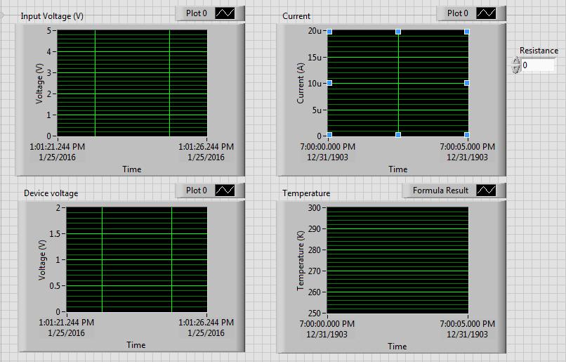
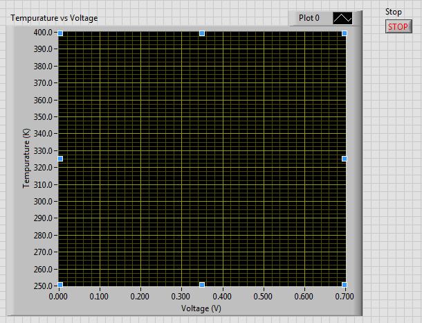
5 37 (4) Where As long as current remains constant, then C is constant, and the activation energy obtained by a linear fit of, such that can be (5) Materials Global Specialties 1310 DC Power Supply SC-2075 Signal Conditioning Board Hotplate 2x Beaker with ice water Type-J Thermocouple wires with banana plug terminals 1n4005 Silicon Diode (or equivalent) in rubber shielding 1n60 Germanium Diode (or equivalent) in rubber shielding Resistance decade box Connecting wires Procedure LabView 1) Open the Characteristic Curve VI 2) Double click on the DAQ Assistant to open it 3) Add another input channel from ai0 and set range to ±50mV 4) Increase the size of the Split Signal block to make 3 outputs 5) Insert the Temperature Formula VI, wire the new input from the split signal to the V input, and place a graph on the Result output 6) Rewire the Build XY Graph so that X input is Device Voltage, and Y input is Result from Temperature Formula 7) Rewire the Error to pass through the Temperature Formula VI 8) Replace the Numeric Constant for resistance to a Numeric Indicator
6 38
 Place one end of the thermocouple in a beaker of ice water 4) Place the second beaker of ice water on the hotplate, submerge the diode and other end of the thermocouple in it 5) Set the DC")
7 39 Procedure - Breadboard 1) Connect the diode and the resistance decade box to the SC-2075 as shown below (same as characteristic lab) 2) Connect the thermocouple wires to CH0+ and CH0- on the SC ) Place one end of the thermocouple in a beaker of ice water 4) Place the second beaker of ice water on the hotplate, submerge the diode and other end of the thermocouple in it 5) Set the DC power supply to 2.5V 6) Run the VI on Labview, and adjust the resistance on the decade box as well as on screen so that the current is at a constant 10µA 7) If initial temperature reading is higher than 273, then switch the two thermocouple leads, and restart the VI 8) Run the VI while heating water, and adjust resistance if necessary to keep constant 10µA 9) Repeat the experiment with the 1N60 Germanium diode END OF ADDITION 6.3. Experimental Equipment
8 40 - Silicon diode with connecting wires - Germanium diode with connecting wires - LabView measuring unit - Hot plate - Thermally insulated jar with dry ice, or liquid nitrogen - Signal generator - Power supply - Digital ammeter - Two beakers with transformer oil. -Thermometer (electronic temperature sensor) 6.4. Procedure 1. Adjust the LabView measuring set-up for measurements current-voltage characteristics using signal generator as a bias source. 2. Connect the measuring set-up to the germanium diode. 2. Set signal generator in linear sweep (triangle pulse) regime at a frequency of 1 Hz with amplitude ±3 V. 3. Obtain current-voltage characteristic of the diode on computer monitor, examine and record it. Make sure that it has a shape of rectifying characteristic shown in Fig Record current-voltage characteristic of the diode at room temperature. Place diode in beaker with oil, wait for half a minute, measure temperature of oil T 1 and take note of forward I F1 and reverse I R1 currents at voltages +2 V and -2 V. 5. Measure conductance of diode at high temperature. Heat beaker with oil to a temperature of 150 C. Immerse diode in oil, wait for half a minute, record current-voltage characteristic, measure temperature of oil and take note of forward and reverse currents at +2 V and -2 V bias. These is another set of data T 2, I F2 and I R2. 6. Measure conductance of diode at low temperature. Place diode in dry ice (liquid nitrogen) together with thermometer (temperature sensor), measure temperature of the cooled diode, record current-voltage characteristic and measure forward and reverse currents at bias +2 V and - 2 V. These is the third set of data T 3, I F3 and I R3. 7. Repeat the whole procedure for silicon diode Calculations and Discussion 1. For each diode, calculate effective activation energy of charge carriers E and coefficient x using formulae (4) and (9) for three combinations of temperature: - room temperature (T 1, I F1 and I R1 ) hot oil. (T 2, I F2 and I R2 );
9 41 - dry ice / liquid nitrogen (T 3, I F3 and I R3 ) room temperature (T 1, I F1 and I R1 ); - dry ice / liquid nitrogen (T 3, I F3 and I R3 ) hot oil (T 2, I F2 and I R2 ). 2. Compare the results. Discuss the reason of change of the activation energy and the coefficient x with temperature. Explain any discrepancies between your experimental results and the expected results. Based on your experimental results, discuss which contribution to the saturation current is dominant in each diode. 3. Discuss whether your measurements give an idea about the working temperature range of silicon and germanium diodes. 4. Discuss possible ways to increase the maximum working temperature of p-n diode. 5. Discuss possible ways to decrease the minimum working temperature on p-n diode. 6. Discuss if it is possible to make p-n diode which could work both at high and low temperatures Questions 1. Why germanium diode is inferior to silicon one in high temperature applications? 2. Why silicon diode is inferior to germanium on in low temperature applications? 3. Which of the two semiconductors (silicon and germanium) is more suitable for high voltage applications and why?
6. Bipolar Diode. Owing to this one-direction conductance, current-voltage characteristic of p-n diode has a rectifying shape shown in Fig. 2.
 36 6. Bipolar Diode 6.1. Objectives - To experimentally observe temperature dependence of the current flowing in p-n junction silicon and germanium diodes; - To measure current-voltage characteristics
7. Bipolar Junction Transistor
 41 7. Bipolar Junction Transistor 7.1. Objectives - To experimentally examine the principles of operation of bipolar junction transistor (BJT); - To measure basic characteristics of n-p-n silicon transistor
EE/COE 152: Basic Electronics. Lecture 3. A.S Agbemenu. https://sites.google.com/site/agbemenu/courses/ee-coe-152
 EE/COE 152: Basic Electronics Lecture 3 A.S Agbemenu https://sites.google.com/site/agbemenu/courses/ee-coe-152 Books: Microelcetronic Circuit Design (Jaeger/Blalock) Microelectronic Circuits (Sedra/Smith)
Digital Integrated Circuits A Design Perspective. The Devices. Digital Integrated Circuits 2nd Devices
 Digital Integrated Circuits A Design Perspective The Devices The Diode The diodes are rarely explicitly used in modern integrated circuits However, a MOS transistor contains at least two reverse biased
Figure 2.1: Energy Band gap Block Diagram
 Figure 2.1: Energy Band gap Block Diagram Figure 2.2: Log Is Vs 10 3 /T Figure 2.3: Schematic Representation of a p-n Junction Diode Department of Physical Sciences, Bannari Amman Institute of Technology,
EXPERIMENT 10: SCHOTTKY DIODE CHARACTERISTICS
 EXPERIMENT 10: SCHOTTKY DIODE CHARACTERISTICS AIM: To plot forward and reverse characteristics of Schottky diode (Metal Semiconductor junction) APPARATUS: D.C. Supply (0 15 V), current limiting resistor
Intrinsic Semiconductor
 Semiconductors Crystalline solid materials whose resistivities are values between those of conductors and insulators. Good electrical characteristics and feasible fabrication technology are some reasons
Electronic Circuits I. Instructor: Dr. Alaa Mahmoud
 Electronic Circuits I Instructor: Dr. Alaa Mahmoud alaa_y_emam@hotmail.com Chapter 27 Diode and diode application Outline: Semiconductor Materials The P-N Junction Diode Biasing P-N Junction Volt-Ampere
CHAPTER 8 The PN Junction Diode
 CHAPTER 8 The PN Junction Diode Consider the process by which the potential barrier of a PN junction is lowered when a forward bias voltage is applied, so holes and electrons can flow across the junction
EE70 - Intro. Electronics
 EE70 - Intro. Electronics Course website: ~/classes/ee70/fall05 Today s class agenda (November 28, 2005) review Serial/parallel resonant circuits Diode Field Effect Transistor (FET) f 0 = Qs = Qs = 1 2π
Electronics I. Midterm #1
 The University of Toledo Section s7ms_elct7.fm - Electronics I Midterm # Problems Points. 4 2. 5 3. 6 Total 5 Was the exam fair? yes no The University of Toledo s7ms_elct7.fm - 2 Problem 4 points For full
Electronic devices-i. Difference between conductors, insulators and semiconductors
 Electronic devices-i Semiconductor Devices is one of the important and easy units in class XII CBSE Physics syllabus. It is easy to understand and learn. Generally the questions asked are simple. The unit
IENGINEERS- CONSULTANTS LECTURE NOTES SERIES ELECTRONICS ENGINEERING 1 YEAR UPTU. Lecture-4
 2 P-n Lecture-4 20 Introduction: If a junction is formed between a p-type and a n-type semiconductor this combination is known as p-n junction diode and has the properties of a rectifier 21 Formation of
Downloaded from
 Question 14.1: In an n-type silicon, which of the following statement is true: (a) Electrons are majority carriers and trivalent atoms are the dopants. (b) Electrons are minority carriers and pentavalent
 Electronic Devices 1. Current flowing in each of the following circuits A and respectively are: (Circuit 1) (Circuit 2) 1) 1A, 2A 2) 2A, 1A 3) 4A, 2A 4) 2A, 4A 2. Among the following one statement is not
Basic Electronics Important questions
 Basic Electronics Important questions B.E-2/4 Mech- B Faculty: P.Lakshmi Prasanna Note: Read the questions in the following order i. Assignment questions ii. Class test iii. Expected questions iv. Tutorials
semiconductor p-n junction Potential difference across the depletion region is called the built-in potential barrier, or built-in voltage:
 Chapter four The Equilibrium pn Junction The Electric field will create a force that will stop the diffusion of carriers reaches thermal equilibrium condition Potential difference across the depletion
Semiconductor Devices Lecture 5, pn-junction Diode
 Semiconductor Devices Lecture 5, pn-junction Diode Content Contact potential Space charge region, Electric Field, depletion depth Current-Voltage characteristic Depletion layer capacitance Diffusion capacitance
UNIT 3 Transistors JFET
 UNIT 3 Transistors JFET Mosfet Definition of BJT A bipolar junction transistor is a three terminal semiconductor device consisting of two p-n junctions which is able to amplify or magnify a signal. It
IENGINEERS- CONSULTANTS QUESTION BANK SERIES ELECTRONICS ENGINEERING 1 YEAR UPTU
 ELECTRONICS ENGINEERING Unit 1 Objectives Q.1 The breakdown mechanism in a lightly doped p-n junction under reverse biased condition is called. (A) avalanche breakdown. (B) zener breakdown. (C) breakdown
Lecture 2 p-n junction Diode characteristics. By Asst. Prof Dr. Jassim K. Hmood
 Electronic I Lecture 2 p-n junction Diode characteristics By Asst. Prof Dr. Jassim K. Hmood THE p-n JUNCTION DIODE The pn junction diode is formed by fabrication of a p-type semiconductor region in intimate
2 MARKS EE2203 ELECTRONIC DEVICES AND CIRCUITS UNIT 1
 2 MARKS EE2203 ELECTRONIC DEVICES AND CIRCUITS UNIT 1 1. Define PN junction. When a p type semiconductor is joined to a N type semiconductor the contact surface is called PN junction. 2. What is an ideal
Laboratory No. 01: Small & Large Signal Diode Circuits. Electrical Enginnering Departement. By: Dr. Awad Al-Zaben. Instructor: Eng.
 Laboratory No. 01: Small & Large Signal Diode Circuits Electrical Enginnering Departement By: Dr. Awad Al-Zaben Instructor: Eng. Tamer Shahta Electronics Laboratory EE 3191 February 23, 2014 I. OBJECTIVES
CHAPTER 8 The PN Junction Diode
 CHAPTER 8 The PN Junction Diode Consider the process by which the potential barrier of a PN junction is lowered when a forward bias voltage is applied, so holes and electrons can flow across the junction
f14m1s_elct7.fm - 1 The University of Toledo EECS:3400 Electronocs I Electronics I Problems Points Total 15 Was the exam fair?
 f4ms_elct7.fm - Electronics I Midterm I Examination Problems Points. 4 2. 5 3. 6 Total 5 Was the exam fair? yes no f4ms_elct7.fm - 2 Problem 4 points For full credit, mark your answers yes, no, or not
Downloaded from
 SOLID AND SEMICONDUCTOR DEVICES (EASY AND SCORING TOPIC) 1. Distinction of metals, semiconductor and insulator on the basis of Energy band of Solids. 2. Types of Semiconductor. 3. PN Junction formation
Chapter 1: Semiconductor Diodes
 Chapter 1: Semiconductor Diodes Diodes The diode is a 2-terminal device. A diode ideally conducts in only one direction. 2 Diode Characteristics Conduction Region Non-Conduction Region The voltage across
EC T34 ELECTRONIC DEVICES AND CIRCUITS
 RAJIV GANDHI COLLEGE OF ENGINEERING AND TECHNOLOGY PONDY-CUDDALORE MAIN ROAD, KIRUMAMPAKKAM-PUDUCHERRY DEPARTMENT OF ECE EC T34 ELECTRONIC DEVICES AND CIRCUITS II YEAR Mr.L.ARUNJEEVA., AP/ECE 1 PN JUNCTION
EJERCICIOS DE COMPONENTES ELECTRÓNICOS. 1 er cuatrimestre
 EJECICIOS DE COMPONENTES ELECTÓNICOS. 1 er cuatrimestre 2 o Ingeniería Electrónica Industrial Juan Antonio Jiménez Tejada Índice 1. Basic concepts of Electronics 1 2. Passive components 1 3. Semiconductors.
Analog Electronic Circuits
 Analog Electronic Circuits Chapter 1: Semiconductor Diodes Objectives: To become familiar with the working principles of semiconductor diode To become familiar with the design and analysis of diode circuits
LAB V. LIGHT EMITTING DIODES
 LAB V. LIGHT EMITTING DIODES 1. OBJECTIVE In this lab you are to measure I-V characteristics of Infrared (IR), Red and Blue light emitting diodes (LEDs). The emission intensity as a function of the diode
Lesson 5. Electronics: Semiconductors Doping p-n Junction Diode Half Wave and Full Wave Rectification Introduction to Transistors-
 Lesson 5 Electronics: Semiconductors Doping p-n Junction Diode Half Wave and Full Wave Rectification Introduction to Transistors- Types and Connections Semiconductors Semiconductors If there are many free
PN Junction Diode Table of Contents. What Are Diodes Made Out Of?
 PN Junction iode Table of Contents What are diodes made out of?slide 3 N-type materialslide 4 P-type materialslide 5 The pn junctionslides 6-7 The biased pn junctionslides 8-9 Properties of diodesslides
Electronics I. Midterm #1
 The University of Toledo Section f6ms_elct7.fm - Electronics I Midterm # Problems Points. 4 2. 5 3. 6 Total 5 Was the exam fair? yes no The University of Toledo f6ms_elct7.fm - 2 Problem 4 points For full
Electronic Circuits I - Tutorial 03 Diode Applications I
 Electronic Circuits I - Tutorial 03 Diode Applications I -1 / 13 - T & F # Question 1 A diode can conduct current in two directions with equal ease. F 2 When reverse-biased, a diode ideally appears as
SEMICONDUCTOR ELECTRONICS: MATERIALS, DEVICES AND SIMPLE CIRCUITS. Class XII : PHYSICS WORKSHEET
 SEMICONDUCT ELECTRONICS: MATERIALS, DEVICES AND SIMPLE CIRCUITS Class XII : PHYSICS WKSHEET 1. How is a n-p-n transistor represented symbolically? (1) 2. How does conductivity of a semiconductor change
REV NO EXPERIMENT NO 1 AIM: To study the PN junction diode characteristics under Forward & Reverse bias conditions. APPARATUS REQUIRED:
 KARNAL INSTITUTE OF TECHNOLOGY & MANAGEMENT KUNJPURA, KARNAL LAB MANUAL OF ------- SUBJECT CODE DATE OF ISSUE: SEMESTER: BRANCH: REV NO EXPERIMENT NO 1 AIM: To study the PN junction diode characteristics
EC6202- ELECTRONIC DEVICES AND CIRCUITS UNIT TEST-1 EXPECTED QUESTIONS
 EC6202- ELECTRONIC DEVICES AND CIRCUITS UNIT TEST-1 EXPECTED QUESTIONS 1. List the PN diode parameters. 1. Bulk Resistance. 2. Static Resistance/Junction Resistance (or) DC Forward Resistance 3. Dynamic
Discuss the basic structure of atoms Discuss properties of insulators, conductors, and semiconductors
 Discuss the basic structure of atoms Discuss properties of insulators, conductors, and semiconductors Discuss covalent bonding Describe the properties of both p and n type materials Discuss both forward
Electronics The basics of semiconductor physics
 Electronics The basics of semiconductor physics Prof. Márta Rencz, Gábor Takács BME DED 17/09/2015 1 / 37 The basic properties of semiconductors Range of conductivity [Source: http://www.britannica.com]
UNIT IX ELECTRONIC DEVICES
 UNT X ELECTRONC DECES Weightage Marks : 07 Semiconductors Semiconductors diode-- characteristics in forward and reverse bias, diode as rectifier. - characteristics of LED, Photodiodes, solarcell and Zener
Digital Electronics. By: FARHAD FARADJI, Ph.D. Assistant Professor, Electrical and Computer Engineering, K. N. Toosi University of Technology
 K. N. Toosi University of Technology Chapter 7. Field-Effect Transistors By: FARHAD FARADJI, Ph.D. Assistant Professor, Electrical and Computer Engineering, K. N. Toosi University of Technology http://wp.kntu.ac.ir/faradji/digitalelectronics.htm
ELECTRONIC DEVICES AND CIRCUITS
 ELECTRONIC DEVICES AND CIRCUITS 1. At room temperature the current in an intrinsic semiconductor is due to A. holes B. electrons C. ions D. holes and electrons 2. Work function is the maximum energy required
Electronics I. Midterm #1
 The University of Toledo s6ms_elct7.fm - Electronics I Midterm # Problems Points. 4 2. 5 3. 6 Total 5 Was the exam fair? yes no The University of Toledo s6ms_elct7.fm - 2 Problem 4 points For full credit,
Ch5 Diodes and Diodes Circuits
 Circuits and Analog Electronics Ch5 Diodes and Diodes Circuits 5.1 The Physical Principles of Semiconductor 5.2 Diodes 5.3 Diode Circuits 5.4 Zener Diode References: Floyd-Ch2; Gao-Ch6; 5.1 The Physical
Università degli Studi di Roma Tor Vergata Dipartimento di Ingegneria Elettronica. Analogue Electronics. Paolo Colantonio A.A.
 Università degli Studi di Roma Tor Vergata Dipartimento di Ingegneria Elettronica Analogue Electronics Paolo Colantonio A.A. 2015-16 Introduction: materials Conductors e.g. copper or aluminum have a cloud
1) A silicon diode measures a low value of resistance with the meter leads in both positions. The trouble, if any, is
 A silicon diode measures a low value of resistance with the meter leads in both positions. The trouble, if any, is") 1) A silicon diode measures a low value of resistance with the meter leads in both positions. The trouble, if any, is A [ ]) the diode is open. B [ ]) the diode is shorted to ground. C [v]) the diode is
1) A silicon diode measures a low value of resistance with the meter leads in both positions. The trouble, if any, is A [ ]) the diode is open. B [ ]) the diode is shorted to ground. C [v]) the diode is
CHAPTER 8 The pn Junction Diode
 CHAPTER 8 The pn Junction Diode Consider the process by which the potential barrier of a pn junction is lowered when a forward bias voltage is applied, so holes and electrons can flow across the junction
EDC Lecture Notes UNIT-1
 P-N Junction Diode EDC Lecture Notes Diode: A pure silicon crystal or germanium crystal is known as an intrinsic semiconductor. There are not enough free electrons and holes in an intrinsic semi-conductor
Electron Devices and Circuits (EC 8353)
") Electron Devices and Circuits (EC 8353) Prepared by Ms.S.KARKUZHALI, A.P/EEE Diodes The diode is a 2-terminal device. A diode ideally conducts in only one direction. Diode Characteristics Conduction Region
Electron Devices and Circuits (EC 8353) Prepared by Ms.S.KARKUZHALI, A.P/EEE Diodes The diode is a 2-terminal device. A diode ideally conducts in only one direction. Diode Characteristics Conduction Region
SRM INSTITUTE OF SCIENCE AND TECHNOLOGY (DEEMED UNIVERSITY)
") SRM INSTITUTE OF SCIENCE AND TECHNOLOGY (DEEMED UNIVERSITY) QUESTION BANK I YEAR B.Tech (II Semester) ELECTRONIC DEVICES (COMMON FOR EC102, EE104, IC108, BM106) UNIT-I PART-A 1. What are intrinsic and
SRM INSTITUTE OF SCIENCE AND TECHNOLOGY (DEEMED UNIVERSITY) QUESTION BANK I YEAR B.Tech (II Semester) ELECTRONIC DEVICES (COMMON FOR EC102, EE104, IC108, BM106) UNIT-I PART-A 1. What are intrinsic and
Physics 281 EXPERIMENT 7 I-V Curves of Non linear Device
 Physics 281 EXPERIMENT 7 I-V Curves of Non linear Device Print this page to start your lab report (1 copy) Bring a diskette to save your data. OBJECT: To study the method of obtaining the characteristics
Lesson 08. Name and affiliation of the author: Professor L B D R P Wijesundera Department of Physics, University of Kelaniya.
 Lesson 08 Title of the Experiment: Identification of active components in electronic circuits and characteristics of a Diode, Zener diode and LED (Activity number of the GCE Advanced Level practical Guide
Department of Electrical Engineering IIT Madras
 Department of Electrical Engineering IIT Madras Sample Questions on Semiconductor Devices EE3 applicants who are interested to pursue their research in microelectronics devices area (fabrication and/or
KOM2751 Analog Electronics :: Dr. Muharrem Mercimek :: YTU - Control and Automation Dept. 1 1 (CONT D) DIODES
 DIODES") KOM2751 Analog Electronics :: Dr. Muharrem Mercimek :: YTU - Control and Automation Dept. 1 1 (CONT D) DIODES Most of the content is from the textbook: Electronic devices and circuit theory, Robert L.
KOM2751 Analog Electronics :: Dr. Muharrem Mercimek :: YTU - Control and Automation Dept. 1 1 (CONT D) DIODES Most of the content is from the textbook: Electronic devices and circuit theory, Robert L.
CHAPTER FORMULAS & NOTES
 Formulae For u SEMICONDUCTORS By Mir Mohammed Abbas II PCMB 'A' 1 Important Terms, Definitions & Formulae CHAPTER FORMULAS & NOTES 1 Intrinsic Semiconductor: The pure semiconductors in which the electrical
Circle the one best answer for each question. Five points per question.
 ID # NAME EE-255 EXAM 1 September 11, 2001 Instructor (circle one) Talavage Gray This exam consists of 16 multiple choice questions and one workout problem. Record all answers to the multiple choice questions
Electronics I. Midterm #1
 EECS:3400 Electronics I s5ms_elct7.fm - Section Electronics I Midterm # Problems Points. 4 2. 5 3. 6 Total 5 Was the exam fair? yes no EECS:3400 Electronics I s5ms_elct7.fm - 2 Problem 4 points For full
Review Energy Bands Carrier Density & Mobility Carrier Transport Generation and Recombination
 Review Energy Bands Carrier Density & Mobility Carrier Transport Generation and Recombination Current Transport: Diffusion, Thermionic Emission & Tunneling For Diffusion current, the depletion layer is
THERMIONIC AND GASEOUS STATE DIODES
 THERMIONIC AND GASEOUS STATE DIODES Thermionic and gaseous state (vacuum tube) diodes Thermionic diodes are thermionic-valve devices (also known as vacuum tubes, tubes, or valves), which are arrangements
Chapter 14 Semiconductor Electronics Materials Devices And Simple Circuits
 Class XII Chapter 14 Semiconductor Electronics Materials Devices And Simple Circuits Physics Question 14.1: In an n-type silicon, which of the following statement is true: (a) Electrons are majority carriers
Section 2.3 Bipolar junction transistors - BJTs
 Section 2.3 Bipolar junction transistors - BJTs Single junction devices, such as p-n and Schottkty diodes can be used to obtain rectifying I-V characteristics, and to form electronic switching circuits
Chapter 2. Diodes & Applications
 Chapter 2 Diodes & Applications The Diode A diode is made from a small piece of semiconductor material, usually silicon, in which half is doped as a p region and half is doped as an n region with a pn
CHAPTER 1 DIODE CIRCUITS. Semiconductor act differently to DC and AC currents
 CHAPTER 1 DIODE CIRCUITS Resistance levels Semiconductor act differently to DC and AC currents There are three types of resistances 1. DC or static resistance The application of DC voltage to a circuit
Unless otherwise specified, assume room temperature (T = 300 K).
.") ECE 3040 Dr. Doolittle Homework 4 Unless otherwise specified, assume room temperature (T = 300 K). 1) Purpose: Understanding p-n junction band diagrams. Consider a p-n junction with N A = 5x10 14 cm -3
ECE 3040 Dr. Doolittle Homework 4 Unless otherwise specified, assume room temperature (T = 300 K). 1) Purpose: Understanding p-n junction band diagrams. Consider a p-n junction with N A = 5x10 14 cm -3
Chapter Semiconductor Electronics
 Chapter Semiconductor Electronics Q1. p-n junction is said to be forward biased, when [1988] (a) the positive pole of the battery is joined to the p- semiconductor and negative pole to the n- semiconductor
AE53/AC53/AT53/AE103 ELECT. DEVICES & CIRCUITS DEC 2015
 Q.2 a. By using Norton s theorem, find the current in the load resistor R L for the circuit shown in Fig.1. (8) Fig.1 IETE 1 b. Explain Z parameters and also draw an equivalent circuit of the Z parameter
ECE-342 Test 1: Sep 27, :00-8:00, Closed Book. Name : SOLUTION
 ECE-342 Test 1: Sep 27, 2011 6:00-8:00, Closed Book Name : SOLUTION All solutions must provide units as appropriate. Use the physical constants and data as provided on the formula sheet the last page of
Shankersinh Vaghela Bapu Institute of Technology INDEX
 Shankersinh Vaghela Bapu Institute of Technology Diploma EE Semester III 3330905: ELECTRONIC COMPONENTS AND CIRCUITS INDEX Sr. No. Title Page Date Sign Grade 1 Obtain I-V characteristic of Diode. 2 To
Digital Integrated Circuits EECS 312
 14 12 10 8 6 Fujitsu VP2000 IBM 3090S Pulsar 4 IBM 3090 IBM RY6 CDC Cyber 205 IBM 4381 IBM RY4 2 IBM 3081 Apache Fujitsu M380 IBM 370 Merced IBM 360 IBM 3033 Vacuum Pentium II(DSIP) 0 1950 1960 1970 1980
Diode as a Temperature Sensor
 M.B. Patil, IIT Bombay 1 Diode as a Temperature Sensor Introduction A p-n junction obeys the Shockley equation, I D = I s e V a/v T 1 ) I s e Va/V T for V a V T, 1) where V a is the applied voltage, V
EE 5611 Introduction to Microelectronic Technologies Fall Thursday, September 04, 2014 Lecture 02
 EE 5611 Introduction to Microelectronic Technologies Fall 2014 Thursday, September 04, 2014 Lecture 02 1 Lecture Outline Review on semiconductor materials Review on microelectronic devices Example of microelectronic
PHYS 3050 Electronics I
 PHYS 3050 Electronics I Chapter 4. Semiconductor Diodes and Transistors Earth, Moon, Mars, and Beyond Dr. Jinjun Shan, Associate Professor of Space Engineering Department of Earth and Space Science and
THE METAL-SEMICONDUCTOR CONTACT
 THE METAL-SEMICONDUCTOR CONTACT PROBLEM 1 To calculate the theoretical barrier height, built-in potential barrier, and maximum electric field in a metal-semiconductor diode for zero applied bias. Consider
ETEK TECHNOLOGY CO., LTD.
 Trainer Model: ETEK DCS-6000-07 FSK Modulator ETEK TECHNOLOGY CO., LTD. E-mail: etek21@ms59.hinet.net mlher@etek21.com.tw http: // www.etek21.com.tw Digital Communication Systems (ETEK DCS-6000) 13-1:
Reg. No. : Question Paper Code : B.E./B.Tech. DEGREE EXAMINATION, NOVEMBER/DECEMBER Second Semester
 WK 5 Reg. No. : Question Paper Code : 27184 B.E./B.Tech. DEGREE EXAMINATION, NOVEMBER/DECEMBER 2015. Time : Three hours Second Semester Electronics and Communication Engineering EC 6201 ELECTRONIC DEVICES
The Semiconductor Diode
 Physics Topics The Semiconductor Diode If necessary, review the following topics and relevant textbook sections from Neamen Semiconductor Physics and Devices, 4th Ed. Section 8.1.5, especially equation
10/27/2009 Reading: Chapter 10 of Hambley Basic Device Physics Handout (optional)
") EE40 Lec 17 PN Junctions Prof. Nathan Cheung 10/27/2009 Reading: Chapter 10 of Hambley Basic Device Physics Handout (optional) Slide 1 PN Junctions Semiconductor Physics of pn junctions (for reference
EE40 Lec 17 PN Junctions Prof. Nathan Cheung 10/27/2009 Reading: Chapter 10 of Hambley Basic Device Physics Handout (optional) Slide 1 PN Junctions Semiconductor Physics of pn junctions (for reference
NAME: Last First Signature
 UNIVERSITY OF CALIFORNIA, BERKELEY College of Engineering Department of Electrical Engineering and Computer Sciences EE 130: IC Devices Spring 2003 FINAL EXAMINATION NAME: Last First Signature STUDENT
Diodes and Applications
 Diodes and Applications Diodes and Applications 2 1 Diode Operation 2 2 Voltage-Current (V-I) Characteristics 2 3 Diode Models 2 4 Half-Wave Rectifiers 2 5 Full-Wave Rectifiers 2 6 Power Supply Filters
Objective Type Questions 1. Why pure semiconductors are insulators at 0 o K? 2. What is effect of temperature on barrier voltage? 3.
 Objective Type Questions 1. Why pure semiconductors are insulators at 0 o K? 2. What is effect of temperature on barrier voltage? 3. What is difference between electron and hole? 4. Why electrons have
LAB V. LIGHT EMITTING DIODES
 LAB V. LIGHT EMITTING DIODES 1. OBJECTIVE In this lab you will measure the I-V characteristics of Infrared (IR), Red and Blue light emitting diodes (LEDs). Using a photodetector, the emission intensity
Basic Electronics Prof. Dr. Chitralekha Mahanta Department of Electronics and Communication Engineering Indian Institute of Technology, Guwahati
 Basic Electronics Prof. Dr. Chitralekha Mahanta Department of Electronics and Communication Engineering Indian Institute of Technology, Guwahati Module: 2 Bipolar Junction Transistors Lecture-1 Transistor
Basic Electronics Learning by doing Prof. T.S. Natarajan Department of Physics Indian Institute of Technology, Madras
 Basic Electronics Learning by doing Prof. T.S. Natarajan Department of Physics Indian Institute of Technology, Madras Lecture 38 Unit junction Transistor (UJT) (Characteristics, UJT Relaxation oscillator,
Chapter Two "Bipolar Transistor Circuits"
 Chapter Two "Bipolar Transistor Circuits" 1.TRANSISTOR CONSTRUCTION:- The transistor is a three-layer semiconductor device consisting of either two n- and one p-type layers of material or two p- and one
SUMMER 13 EXAMINATION Subject Code: Model Answer Page No: / N
 Important Instructions to examiners: 1) The answers should be examined by key words and not as word-to-word as given in the model answer scheme. 2) The model answer and the answer written by candidate
Section:A Very short answer question
 Section:A Very short answer question 1.What is the order of energy gap in a conductor, semi conductor, and insulator?. Conductor - no energy gap Semi Conductor - It is of the order of 1 ev. Insulator -
CONTENTS. 2.2 Schrodinger's Wave Equation 31. PART I Semiconductor Material Properties. 2.3 Applications of Schrodinger's Wave Equation 34
 CONTENTS Preface x Prologue Semiconductors and the Integrated Circuit xvii PART I Semiconductor Material Properties CHAPTER 1 The Crystal Structure of Solids 1 1.0 Preview 1 1.1 Semiconductor Materials
 Energy band diagrams Metals: 9. ELECTRONIC DEVICES GIST ρ= 10-2 to 10-8 Ω m Insulators: ρ> 10 8 Ω m Semiconductors ρ= 1 to 10 5 Ω m 109 A. Intrinsic semiconductors At T=0k it acts as insulator At room
Lecture 4 -- Tuesday, Sept. 19: Non-uniform injection and/or doping. Diffusion. Continuity/conservation. The five basic equations.
 6.012 ELECTRONIC DEVICES AND CIRCUITS Schedule -- Fall 1995 (8/31/95 version) Recitation 1 -- Wednesday, Sept. 6: Review of 6.002 models for BJT. Discussion of models and modeling; motivate need to go
Experiment Topic : FM Modulator
 7-1 Experiment Topic : FM Modulator 7.1: Curriculum Objectives 1. To understand the characteristics of varactor diodes. 2. To understand the operation theory of voltage controlled oscillator (VCO). 3.
Sharjah Indian School, Sharjah ELECTRONIC DEVICES - Class XII (Boys Wing) Page 01
 Page 01") ELECTRONIC DEVICES - Class XII (Boys Wing) Page 01 Electronics is the fast developing branch of Physics. Before the discovery of transistors in 1948, vacuum tubes (thermionic valves) were used as the building
ELECTRONIC DEVICES - Class XII (Boys Wing) Page 01 Electronics is the fast developing branch of Physics. Before the discovery of transistors in 1948, vacuum tubes (thermionic valves) were used as the building
Difference between BJTs and FETs. Junction Field Effect Transistors (JFET)
") Difference between BJTs and FETs Transistors can be categorized according to their structure, and two of the more commonly known transistor structures, are the BJT and FET. The comparison between BJTs
Difference between BJTs and FETs Transistors can be categorized according to their structure, and two of the more commonly known transistor structures, are the BJT and FET. The comparison between BJTs
R a) Draw and explain VI characteristics of Si & Ge diode. (8M) b) Explain the operation of SCR & its characteristics (8M)
 Draw and explain VI characteristics of Si & Ge diode. (8M) b) Explain the operation of SCR & its characteristics (8M)") SET - 1 1. a) Define i) transient capacitance ii) Diffusion capacitance (4M) b) Explain Fermi level in intrinsic and extrinsic semiconductor (4M) c) Derive the expression for ripple factor of Half wave
SET - 1 1. a) Define i) transient capacitance ii) Diffusion capacitance (4M) b) Explain Fermi level in intrinsic and extrinsic semiconductor (4M) c) Derive the expression for ripple factor of Half wave
Student Lecture by: Giangiacomo Groppi Joel Cassell Pierre Berthelot September 28 th 2004
 Student Lecture by: Giangiacomo Groppi Joel Cassell Pierre Berthelot September 28 th 2004 Lecture outline Historical introduction Semiconductor devices overview Bipolar Junction Transistor (BJT) Field
Photodiode: LECTURE-5
 LECTURE-5 Photodiode: Photodiode consists of an intrinsic semiconductor sandwiched between two heavily doped p-type and n-type semiconductors as shown in Fig. 3.2.2. Sufficient reverse voltage is applied
UNIVERSITY OF CALIFORNIA AT BERKELEY College of Engineering Department of Electrical Engineering and Computer Sciences.
 UNIVERSITY OF CALIFORNIA AT BERKELEY College of Engineering Department of Electrical Engineering and Computer Sciences Discussion #9 EE 05 Spring 2008 Prof. u MOSFETs The standard MOSFET structure is shown
Class XII - Physics Semiconductor Electronics. Chapter-wise Problems
 lass X - Physics Semiconductor Electronics Materials, Device and Simple ircuit hapter-wise Problems Multiple hoice Question :- 14.1 The conductivity of a semiconductor increases with increase in temperature
Semiconductor Physics and Devices
 Metal-Semiconductor and Semiconductor Heterojunctions The Metal-Oxide-Semiconductor Field-Effect Transistor (MOSFET) is one of two major types of transistors. The MOSFET is used in digital circuit, because
Lab 2: Linear and Nonlinear Circuit Elements and Networks
 OPTI 380B Intermediate Optics Laboratory Lab 2: Linear and Nonlinear Circuit Elements and Networks Objectives: Lean how to use: Function of an oscilloscope probe. Characterization of capacitors and inductors